Choose timezone
Your profile timezone:
The International Workshops on Radiation Imaging Detectors are held yearly and provide an international forum for discussing current research and developments in the area of position sensitive detectors for radiation imaging, including semiconductor, gas and scintillator-based detectors. Topics include processing and characterization of detector materials, hybridization and interconnect technologies, design of counting or integrating electronics, readout and data acquisition systems, and applications in various scientific and industrial fields. The workshop will have plenary sessions with invited and contributed papers presented orally and in poster sessions. The invited talks will be chosen to review recent advances in different areas covered in the workshop.



In the early 1990’s scientists and engineers at CERN were taking the first steps in developing hybrid pixel detectors for use at the future Large Hadron Collider. As part of the quality control procedure for the bump bonding interconnect of those early devices, the detectors were exposed to X-rays. The devices had to be triggered electronically, the selected events read out, and the binary images added up in software. It was relatively small step to replace the on-pixel delay and trigger logic with a particle counter while changing the pixel geometry from rectangular to square. This became the Medipix1 or Photon Counting chip. Over the ensuing 30 years or so, the Medipix Collaborations have benefitted from CMOS technology scaling to bring more-and-more hit processing onto each pixel. The Timepix4 chip, for example, can tag events to ~200ps at the pixel level while providing triggerless readout at rate of up to 358 Mhits/cm2/sec.
This presentation will review the major technical and organisational milestones which not only permitted advances in the architecture of the readout chips but also promoted their dissemination to numerous fields of research. The presentation will be peppered with images of, among other things, human body parts, watches, insects and even cats!
The Analog Spectral Imager for X-rays (ASIX) is a technology demonstrator for a 50 𝜇m pixel Hybrid Pixel Detector (HPD), with fully-analog single photon processing readout. ASIX aims at delivering simultaneous energy and spatial high resolution at the best achievable count rate.
By combining fine-pitch (50𝜇m hexagonal) and an ultra-low noise (<30 𝑒− ENC) fully-analog pixel readout with a self-triggering logic capable of precisely isolating all the pixels belonging to the charge cluster, ASIX aims to work around the charge sharing problem, exploiting it to provide significant sub-pixel resolution for energy resolved X-ray imaging. A preliminary successful evaluation of this statement has been conducted on an early version of the demonstrator made by coupling a readily available readout chip with 50𝜇m hexagonal pixels to a 300 𝜇m thick silicon n-on-p sensor developed at FBK. For this ASIX proof-of-concept detector, we estimated a 7 𝜇m spatial resolution along with ∼600 eV (FWHM, at 9.7 keV) energy resolution, the last being dominated by the electronics noise (70 e− ENC).
We recently developed a prototype for a new readout chip in a commercial 65 nm CMOS process. This prototype chip implements a fully functional 8×16 ASIX pixels matrix with cluster-based readout. Each pixel includes its own low-noise (<30 e− ENC) spectroscopic electronics chain followed by a discriminator, with local 5-bit DAC for individual pixel threshold fine tuning, and a Peak Detector. Pixels include selectable 50 fF and a 100 fF capacitors emulating the sensor pixel along with a precise test charge injection circuit, allowing realistic performance evaluation in terms of noise and pixel response function.
This prototype pixel matrix we will use as the main building block for the final ASIX HPD demonstrator.
We will present the basic concept of the ASIX approach and
test results from the prototype readout chip.
More details and figures are provided in the attached summary.
Modern storage ring light sources require new detector concepts to allow x-ray scientists to thoroughly exploit the higher brilliance and explore state-of-the-art beam modulations, such as continuous-wave operation. A broad range of collaborations is targeting the advances on the readout chain to enable fast readout with nearly zero dead-time [1], [2], [3]. In parallel, data acquisition processes which ensure that the massive stream of data is properly read out are actively being developed, such as new compression techniques [4] and several hundred gigabit transmission hardware and protocols [5].
Within this framework, the AlpRay collaboration — a partnership between DECTRIS AG Ltd., University of Bergamo and University of Pavia — was established to develop a compact readout processor in a commercial 110 nm CMOS technology for hybrid detectors, to be used in applications at fourth-generation synchrotrons, FEL, or in electron microscopes with pulsed electrons. The designed analog readout channel supports both a continuous-wave and pulsed operations. A medium dynamic range of 100 photons (1000 in a secondary mode) at 8 keV is expected at the input. The readout chain ensures an SNR > 5 and provides an expected readout rate of about 100 kcps per pixel, with a dead time of 1 – 2%. The architecture is designed to enable scaling the rate toward 1 Mcps per pixel in a future iteration, while keeping the same processing chain. The target pixel pitch is 75 μm and a 256 x 256 matrix is expected for the final prototype, covering an area of 20 x 20 mm2 with a power density of ~.5 W/cm2. The core development is focused on ensuring a linear input/output characteristic of the channel over the whole input dynamic range, in order to avoid excessive complications in the channel calibration procedure.
The architecture envisioned for the readout chain is reported in Figure 1. A charge sensitive amplifier (CSA) interfaces with the electron-collecting detector bump-bonded to the front-end. The forward gain stage is based on a cascode stage with a push-pull class B output stage, providing a ~800 mV linear output dynamic range and two modes: a high-gain one for a maximum dynamic range of 100 photons, guaranteeing SNR > 5, and a low-gain counterpart that enhances the dynamic range to 1000 photons, with lower SNR. Following the CSA is a flip-capacitor sample and hold (S/H) stage based on an operational amplifier with a rail-to-rail input stage and a push-pull AB output stage. The A/D conversion is performed by a timestamp-based Wilkinson ADC: a discriminator chain compares the S/H output with a peripherally-generated ramp, and a distributed Gray-code-based timestamp is latched with the hit of the discriminator, providing a timestamp proportional to the readout charge. A compression mode can be selected for the Wilkinson ADCs to speed up the conversion process at the cost of a coarser digitization for high photon inputs. The compression acts on the reference ramp, changing the slope of it after a programmable threshold is reached.
A time diagram of the readout chain is provided in Figure 2. In the plot, the response of the circuit to a random-amplitude pulsed input with a period of 1 us is reported. For each pulse arriving from the detector, the CSA generates a proportional positive voltage step. These steps are integrated over a specific exposure time of about 10 us, after which the CSA is reset. Just before the reset, the level reached by the CSA output is sampled by the S/H and held for the entire duration of the following frame. In this way, while the ADC digitises the previous frame, a new train of pulses is integrated by the CSA, ensuring a dead-time dependent only on the S/H sampling phase and settling time, which in the reported plot is approximately 100 ns.
The whole architecture has been simulated in the different modes, for all the expected input signals, and verified in corners and Montecarlo simulations. The layout of the pixel is ongoing and a submission is expected by Q2 2027. The prototype envisioned for the first run is a 256 x 256 fully-populated pixel matrix including some test structures to characterise the individual blocks of the front-end electronics.
[1] N. Zhou Hagström et al., “Megahertz-rate ultrafast X-ray scattering and holographic imaging at the European XFEL,” J. Synchrotron Radiat., vol. 29, no. 6, pp. 1454–1464, Nov. 2022, doi: 10.1107/S1600577522008414.
[2] L. Gaioni, A. Galliani, L. Ratti, V. Re, and G. Traversi, “A 28 nm CMOS front-end circuit with in-pixel flash ADC for high-rate hybrid detectors,” Nucl. Instrum. Methods Phys. Res. Sect. Accel. Spectrometers Detect. Assoc. Equip., vol. 1080, p. 170655, Nov. 2025, doi: 10.1016/j.nima.2025.170655.
[3] P. Lazzaroni et al., “Analog Readout Channel for Continuous-Wave X-Ray Science Applications,” IEEE Trans. Nucl. Sci., vol. 72, no. 6, pp. 1959–1968, Jun. 2025, doi: 10.1109/TNS.2025.3565911.
[4] R. Rasheedi et al., “A 28 nm multiply-accumulate ASIC architecture for on-chip data compression in MHz frame rate X-ray and electron pixel detectors,” J. Instrum., vol. 20, no. 10, p. P10027, Oct. 2025, doi: 10.1088/1748-0221/20/10/P10027.
[5] G. Ciarpi, G. Atzeni, A. Klekotko, S. Biereigel, P. Moreira, and S. Kulis, “Design of a 25 Gb/s high-voltage radiation-tolerant driver for SiPh modulators in 28 nm CMOS technology,” J. Instrum., vol. 21, no. 03, p. C03009, Mar. 2026, doi: 10.1088/1748-0221/21/03/C03009.
The authors acknowledge funding from DECTRIS AG Ltd.
Grab a coffee, and e-meet your colleagues in the gather.town platform
Traditional medical imaging systems depend on X-ray absorption differences among tissues to distinguish them [1]. While effective at separating bones from other biological structures, they struggle to differentiate between different types of soft tissue (e.g., normal and tumor cells) [2]. The refractive properties of tissues, however, can induce X-ray phase shifts that are highly sensitive to subtle changes in their composition [3]. Encoding this extra information into the detector enables the visualization of soft tissue boundaries with high contrast. To this end, the 1MICRON1 project has been proposed, with the aim of developing a system that can facilitate phase contrast imaging using its ultra-high spatial resolution of the order of 1 µm. We are developing a new Monolithic Active Pixel Sensors (MAPS) that can reach the high spatial resolution that is required in phase contrast imaging applications. Benefiting from the success of the ARCADIA project [4], the sensors have been further engineered to accommodate thick substrates (≥ 500 µm) for higher X-ray absorption efficiency, and different sensor designs to allow for comprehensive evaluation of their functional performance. Moreover, as a valuable lesson learnt from the ARCADIA project, we started by designing different edge structures, which play a crucial role in determining the sensor’s electrical behavior. Breakdown voltage is particularly critical, especially after irradiation-induced
surface damage, which introduces a significant amount of positive oxide charge in the SiO2 over the sensor’s operational lifetime. To this end, we performed a series of TCAD simulations to determine the sensor’s electrical properties (e.g., punch-through, breakdown) for different edge structures. Figure 1 shows the schematics of the device under study, highlighting edge structures consisting of an edge Pwell,
floating Pwells, N guard rings, and the sensor itself, which comprises Pwell and Collection Nwell regions. Simulation results show that with a
proper Pwell configuration (e.g., number of Floating Pwells and the
associated spacing and width) the sensor can reach full depletion before
the onset of punch-through, and there is a large margin between the
breakdown voltage and the operation voltage. However, the breakdown
voltage gradually decreases after surface damage, eventually becoming lower than the full depletion voltage at the highest positive oxide charge considered (~1×10¹²/cm2). To overcome this limitation, the edge structure has been optimized by adding extra Floating Pwells and introducing field plates; results show that, with these additional features, the sensor can reach full depletion without risk of electrical breakdown. Furthermore, with the help of the MonteCarlo simulation platform Allpix2, charge-sharing effects have also been assessed to evaluate the sensor’s spatial and temporal resolution.
The High Energy upgrade of the Linac Coherent Light Source II (LCLS-II-HE) at SLAC National Accelerator Laboratory will deliver X-ray pulses at repetition rates up to 1 MHz, placing stringent requirements on detector systems [1]. SLAC’s phased detector development roadmap [2] produces X-ray detectors based primarily on silicon sensors bump-bonded to custom readout ASICs. The ePixUHR ASIC, featuring a 192×168 pixel matrix with 100 μm pixel pitch and 12-bit dynamic range, addresses the 35 to 100 kHz (the latter rate will use a revised version of the same ASIC) frame-rate tier.
Some scientific campaigns at experimental beamlines such as X-ray Pump and Probe (XPP), Coherent X-ray Imaging (CXI) and Macromolecular Femtosecond Crystallography (MFX) require large focal planes ranging from 4 to 16 megapixels; The design of these large-area detectors is presented. They are built as segmented assemblies, and the fundamental building block of the system is a 2×3 carrier and readout board (Figure 1) that integrates one silicon sensor with six ePixUHR ASICs operating continuously at 35,000 frames per second (fps). Six 2×3 modules are combined into a self-sufficient 1 megapixel tile (Figure 2) that consolidates power distribution, liquid cooling and data aggregation into a standalone unit, simplifying system integration and enabling modular scaling. Four 1 megapixel modules (1M) form the full 4 megapixel (4M) detector, delivering continuous 35,000 fps operation across all ASICs. This architecture is readily extendable and a 16 megapixel configuration is currently in design.
Each readout board connects to the data acquisition system via a fiber bundle of 12 bidirectional lanes: eight lanes carry detector data using the HTSP [4] protocol as two 100 Gbit/s links (four lanes each at 25 Gbit/s), one lane provides timing synchronization, one lane handles configuration, and two lanes are reserved for transmitting on-detector processed data to edge compute nodes for fast feedback and trigger generation using AI and classical algorithms.
The firmware is developed using SURF [5] and ROGUE [6] open-source libraries and follows the architecture shown in Figure 3. A critical challenge for x-ray detectors operating at 35,000 fps is the need to descramble and calibrate every frame in real time within the readout FPGA before the data leaves the detector. At these rates real-time calibration is essential to enable downstream algorithms including, for example, machine learning-based in firmware hit classification (similar to the work present in [3]) to operate directly on the data stream without offline pre-processing. To address this, an HLS-based processing core performs dark subtraction and linear gain equalization concurrently across all six ASICs served by a single FPGA. A design space exploration (DSE) was performed to identify the optimal trade-off between throughput and FPGA resource utilization. The selected configuration achieves 53 kHz throughput comfortably above the 35,000 fps operating rate while consuming 45% of available BRAM and only 10% of DSP resources on the detector FPGA, leaving substantial headroom for future processing stages.
The detector is currently under fabrication, but bare ASICs as well as all carrier boards, readout boards and mechanical systems have been successfully characterized and validated. The first 2×3 module with bump-bonded silicon sensors has been received, and end-to-end tests will soon be performed. Results from laboratory testing and from the MFX instrument will be reported at the conference.
References
[1] R. Schoenlein et al., 2016 Technical Report. https://doi.org/10.2172/1634206.
[2] H. Sandberg et al., 2025 JINST 20 P08019
[3] T.-W. Ke et al., (2018). J. Synchrotron Rad. 25, 655-670.
[4] L. Ruckman and D. Doering 2022 JINST 17 P07026
[5] SLAC, SURF: SLAC Ultimate RTL Framework, https://github.com/slaclab/surf (2026).
[6] SLAC, Rogue: SLAC Python Based Hardware Abstraction & Data Acquisition System, https://github.com/slaclab/rogue (2026).
Acknowledgments
R&D at the Linac Coherent Light Source (LCLS), SLAC National Accelerator Laboratory, is supported by the U.S. Department of Energy, Office of Science, Office of Basic Energy Sciences under Contract No. DE-AC02-76SF00515
The JUNGFRAU chip was originally developed for applications in the hard and tender X-ray range at free-electron lasers (XFEL) and high-flux synchrotron sources. It employs a charge-integrating architecture with three dynamically switching gains to achieve the large dynamic range required in these environments. In its highest gain setting and at a 5 µs integration time, the current version—JUNGFRAU 1.2—has a noise of 31 electrons r.m.s. (≈ 110 eV equivalent energy in silicon) at room temperature [1]. This low noise enables single-photon detection down to the upper end of the soft X-ray range (≥ 600 eV).
By combining JUNGFRAU with inverse low-gain avalanche diode (iLGAD) sensors, which provide intrinsic gain and a thin entrance window enabling high quantum efficiency (> 85% at 250 eV) [2,3], a signal-to-noise ratio > 5 has been demonstrated for single-photon detection down to 400 eV [2,4]. Extending the operating range to lower energies, in particular into the “water window” (280–530 eV, between the C and O K-edges), requires further improvements. To this end, we pursue both sensor optimizations and ASIC developments.
Here, we focus on the ASIC and introduce a dedicated low-noise version of JUNGFRAU 1.2. In a first design iteration, the dynamic gain switching circuitry is disabled, reducing parasitic capacitances at the cost of dynamic range. This modification lowers the noise from 31 to 26 electrons r.m.s. (−16%) at a 5 µs integration time. We describe the implemented design modifications and evaluate noise and single-photon detection performance in combination with iLGAD sensors and silicon sensors with optimized entrance windows. We conclude with an outlook on further improvements toward a dedicated low-noise JUNGFRAU ASIC for soft X-ray applications.
[1] V Kedych et al., in preparation
[2] J Zhang et al., JINST 17 (2022), C22011
[3] M Carulla et al., Sensors 24 (2024), 942
[4] A Liguori et al., JINST 18 (2023), P12006
The authors acknowledge funding from the Swiss National Science Foundation (SNSF) [PZ00P2_223377]. For the purpose of open access, a CC BY public copyright license is applied to any author accepted manuscript (AAM) version arising from this submission.
Ion therapy with protons or heavier particles like helium or carbon enables highly precise and conformal dose delivery within the target volume, especially in comparison to photon-based radiation therapy. However, this precision is associated with a higher treatment sensitivity to anatomical and positional changes of the patient [1]. To detect such changes, our group developed a monitoring method for carbon ion therapy. After extensive experimental studies, the method is now in its third year of clinical trial called In Vivo Monitoring (InViMo). In addition to carbon ion treatments, its application to irradiations with helium ions is being explored, with first patient measurements showing promising results [2].
For the monitoring process, a customized tracking system consisting of seven mini-trackers has been developed. Each tracking module consists of two pairs of Timepix3 hybrid silicon pixel detection layers. During irradiation, carbon ions interact with the tissue in their path and charged nuclear fragments are produced. With our detection system, these secondary particles are recognized and their tracks can be reconstructed. Thus, the location of the fragmentation vertices can be determined. By comparing measurements across treatment days, changes in signal distributions can indicate anatomical or positional variations of the patient [3].
In this contribution, the potential of monitoring in helium ion beam therapy is evaluated by comparing its secondary ion fluence to that obtained during carbon ion beam therapy. Measurements were performed on a head-like model with and without induced anatomical changes. Using identical, clinically realistic treatment beams enables a direct comparison between the two ion species.
As expected for helium ions, the detected fragment yield was found to be generally lower than in the irradiation with carbon ions at the same treatment dose. Nevertheless, both ion types show clear signal differences in response to the induced anatomical change. For helium, this signal is particularly strong, suggesting a promising potential for the method in monitoring helium ion therapy.
[1] Muraro et al., Frontiers in Oncology, 6, 177 (2016)
[2] Kelleter et al., Int. J. Radiat. Oncol. Biol. Phys. (2026), S0360-3016
[3] Schweins et al., Medical physics, 52, 4 (2025), 399–2411
Recent advances in 4D tracking detectors have enabled time-of-flight ion computed tomography (TOF-iCT), an imaging modality designed to improve dose conformity and reduce range uncertainties in ion beam therapy. By measuring the particle path and TOF of therapeutic ions traversing the patient, TOF-iCT enables the reconstruction of a precise stopping power (SP) map. The accuracy of this map is critical for effective treatment planning.
In this work, we report the development of a TOF-iCT demonstrator comprising 12 single-sided low-gain avalanche diode (LGAD) strip detectors. The system can be operated either in combination with a TOF calorimeter or in a sandwich TOF-iCT configuration. Imaging studies were performed in both ex vivo and in vivo settings using small mice, providing insight into system performance under realistic experimental conditions. In addition, challenges related to high-rate 4D tracking of multiple ion species and the identification of nuclear fragments are discussed.
The increasing complexity of modern nuclear imaging systems, in particular of Total-Body PET scanners, is mainly driven by the large number of readout channels. This results in significant power consumption, increased system complexity and scalability limitations. In conventional architectures, signals from arrays of photodetectors must be acquired, digitized, and processed, leading to a substantial energy overhead. To mitigate these issues, there is a growing interest in moving signal processing closer to the sensor front-end, achieving detector with internal pre-processing. This approach reduces interconnect complexity, bandwidth requirements, and overall power consumption.
However, although flexible, traditional FPGA-based solutions are not well-suited to such highly parallel systems, due to the energy costs of high-speed ADCs. In this context, analog neural networks represent a promising alternative, as they allow for reducing the number of signal domain conversions [1].
To explore this approach, we have developed the second version of ANNA (Analog Neural Network ASIC) [2], a dedicated chip designed for scintillator-based emission tomography detectors (Fig. 1). This implements a capacitive, fully connected, 5-layer analog neural network designed to estimate the interaction coordinates (x,y) of gamma photons in a monolithic scintillator, reducing the number of analog signals to be digitized from 64 to 2. It is based on a configurable network of 2240 neurons with capacitive weights (Fig. 2) that can process 64 channels from a front-end ASIC reading a standard 8 × 8 SiPM array adopted in emission tomography (and potentially realized on the same CMOS chip). The network operates entirely in the analog domain, summing signals in charge mode and including non-linear activation functions. For this reason, training is performed offline in TensorFlow using a model derived from circuit characterization, allowing to account non-idealities [3]. The architecture is programmable with a maximum depth of five layers and 6-bit quantized weights. It is also able to support up to 32 outputs, in order to widen the use cases beyond PET.
Cadence circuit simulations were carried out to validate the architecture and power consumption. The power drawn by ANNA is ≈800 μW (with a 20 MHz clock, setting an inference time of ≈1.5 μs) confirming competitive energy efficiency. A single-event inference at the schematic level shows good agreement with expected results, with an Euclidean error of 4.7 mV (corresponding to ≈0.2 mm error over a 50 mm-side Scintillator). Preliminary experimental measurements on fabricated ASIC (Fig.3) tested a single network layer, confirming these results and showing output voltages consistent with both simulations and model predictions, thus providing an initial experimental validation of the proposed approach.
[1] K. Gong, et al., Proc. IEEE 108 (2020), 51-68.
[2] S. Di Giacomo, et al. IEEE Trans. Rad. Pl. Med. Sci. 9 (2025) 542-552.
[3] M. Ronchi, et al. IEEE Trans. Circ. Sys. I 8 (2025) 3947-3960.
γ-cameras with coded apertures have been proved to be an efficient method to identify weak γ-radioactive sources in three-dimensional space, providing planar images with sufficient spatial resolution and signal-to-noise ratio [1]. In this work, we attempted a single-photon-emission computerized tomography with the filtered-back-projection method, exploiting planar images derived by a fast-simulation code. The field of view (FOV) comprised by the system is specifically designed for human-centric applications, focusing on the accurate three-dimensional localization of radioactive tracers within the human body for clinical diagnostics. The evaluation of the method has been done via the appropriate figures of merit like the source-location-accuracy, the signal-to-noise ratio (SNR) and the full width at half maximum (FWHM) of the point-spread function.
Planar images of the simulated radioactive sources are captured by rotating the mask-detector system around the origin of coordinates, with motion constrained to the x-z plane. Coded aperture comprised by arranging lead spheres on a transparent plate in a Modified Uniformly Redundant Array (MURA) mask configuration [2]. The system is evaluated in a near-field geometry —a configuration essential for medical settings where source-to-detector distances are limited— with the detector and the mask positioned 860 mm and 820 mm from the center of rotation, respectively. The radioactive sources placed in the whole range of FOV even at the edge, i.e. (230, 230, 230) mm, demonstrating high-fidelity tomographic images.
The reconstruction process is based on 3D back-projection, while a Ram-Lak filter is incorporated to mitigate the ambiguity and artifacts introduced by simple back-projection. Both point and extended radioactive sources are examined, with the latter being geometrically approximated as rectangular parallelepipeds to simulate distributions of radioactivity in human tissues. The quantitative results demonstrate the system's ability to accurately reconstruct radioactivity distributions and distinguish between various source configurations, providing a robust computational foundation for high-resolution 3D medical diagnostic imaging with modified uniformly redundant array (MURA) coded apertures []. For tomographic images, a point source at the center of rotation yields an SNR of 18 and a FWHM of 50 mm, whereas at the eccentric position (230, 230, 230) mm the SNR is 17.5 with a FWHM of 54 mm, indicating that the 3D back-projection method maintains adequate reconstruction fidelity even at off-center source locations approaching the edge of the field of view.
[1] I. Kaissas et al 2020 JINST 15 C01012
[2] Stephen R. Gottesman and E. E. Fenimore, Appl. Opt. 28, 4344-4352 (1989)
During energy-dispersive X-ray diffraction, the sample is irradiated with a pencil beam generated by a standard polychromatic X-ray tube without any spectral filtering. Two-dimensional polychromatic diffraction images are acquired using a Timepix 3 quad CdTe detector with a central aperture to allow the pencil beam to pass through without parasitic interaction. The detector, equipped with a USB3 interface, has a throughput of up to 47 Mcts/s. For each detected photon, its position is known with an accuracy of 55 µm in the detector plane, and its energy with a resolution of 4 keV at 60 keV. The recorded polychromatic data are then converted into an equivalent monochromatic XRD pattern that would result from the use of a monochromatic X-ray source. For a detailed analysis of the XRD pattern, it was necessary to remove undesirable photons resulting from scattering and, above all, from internal XRF from the sensor material. It will be shown that the resulting XRD patterns reveal a wealth of information.
Thanks to the 160 kV voltage of the X-ray tube, the polychromatic narrow beam was able to pass through a highly attenuating sample of 1.5 mm thick steel sheet. By utilizing the entire X-ray spectrum, the beam has sufficiently high intensity to obtain XRD patterns quickly enough even when investigating relatively fast physical processes. It has been verified that a temporal resolution of 0.01 s can be achieved with this setup. This allows for the analysis of phase transitions in a polycrystalline sample during its heat treatment under standard laboratory conditions, which is otherwise only possible at synchrotron sources [1]. The ability to examine relatively large samples throughout their volume makes it possible to investigate other time-dependent phenomena that do not manifest themselves on the sample’s surface, such as changes in the lattice dimensions of steel due to hydrogen diffusion.
[1] Vavrik, D., Georgiev, V., Jakubek, J. et al. Sci Rep 15, 31752 (2025). https://doi.org/10.1038/s41598-025-16314-9
The institutional support of RVO68378297 is kindly acknowledged.
Introduction
Delivering Carbon-ion radiotherapy (CIRT) at consistently high accuracies throughout a multi-week treatment remains challenging in clinical practice. Even though the dose conformity of CIRT is exceptionally high, it always relates to the last known factual state of the patient’s anatomy, which gets increasingly uncertain the more time has passed since the Computed Tomography (CT) imaging for dose planning was acquired. Since current treatment guidelines often include at most weekly control imaging throughout a multi-week therapy, our goal is to update the knowledge about the state of the patient anatomy at daily intervals. Detecting clinically significant changes between treatment fractions can support clinicians in authorizing additional imaging to adapt the treatment plan when necessary.
Our group’s approach to obtaining additional evidence about anatomical changes is to detect nuclear fragments, emitted during irradiation, with Timepix3 detectors and reconstructing their point of origin [1]. The spatial distribution of secondary radiation has been shown to carry significant information about the treated region and we develop methods capable of exploiting it to perform in vivo monitoring. The goal is to detect and localize anatomical changes between treatment days and extract their 3D volume and shape information for further evaluation. This will support reducing the reliance on conventional imaging modalities such as CT, which involves additional resources and radiation exposure for the patient.
Materials and Methods
Our approach is based on our recently published method for detecting the depth of anatomical changes along the beam axis by exploiting joint frequency band variations of projection differences [2]. At the center of our method, a distinct correlation matrix enables identifying local similarities and consequently distinguishing between the target region, i.e. the locations of the changes, and the background.
We extract the required 3D information about potential anatomical changes by performing the same depth (z) analysis consecutively for all nuclear fragment subsets contained in a moving window in the transverse plane (x,y). Joining the window locations with the detected depth yields the 3D reconstructed locations of anatomical change. This splitting of the original set of reconstructed nuclear fragment origins into smaller subsets for analysis has the consequence that each subset exhibits a statistically less stable distribution. Given the already challenging signal-to-noise ratio when comparing measurements from different treatment fractions, reducing the available number of fragment origins makes robust detection and localization increasingly challenging.
We therefore trained a deep-learning model with the aim of determining the depth of anatomical changes based on classifying correlation matrices to support our reconstruction pipeline. The method treats the depth approximation as an image classification problem, exploiting high-dimensional information extracted from this already enriched data source and compressing it further into a neural network model (ResNet, RegNet or ConvNeX architectures) which performs its own depth approximation. Both results are subsequently joined into a common 3D reconstruction.
Results
We validated our 3D reconstructions on measurements acquired during dedicated experiments with Polymethyl Methacrylate (PMMA) head sized phantoms conducted at the Heidelberg Ion Beam Therapy Center (HIT). Our experimental setups contained coin-shaped air cavities of 20 mm diameter placed at varying depths and lateral locations of the phantom. These controlled setups allowed a detailed qualitative and quantitative assessment of the method in terms of reconstruction loss versus the known 3D setups. We report the results at varying depths, with a mean absolute error over the region of interest starting from <3 mm and Jaccard Index (intersection over union, or ‘IoU’) values peaking at >0.8 within the region of interest when considering the exact 3D location of the cavity. We show that our framework is capable of highly accurate 3D reconstruction of anatomical changes, including retaining the principal location and shape of the change region.
Conclusion
Our results show that we can achieve full 3D reconstruction of anatomical changes based only on the information carried by nuclear fragments emerging from the phantom. We have shown that despite the small number of available data sets for training, it is possible to extract sufficiently localized information to successfully train modern deep-learning models to serve as supporting methods and surrogates useful in stabilizing statistical variations. Mapping the exact locations to those of the actual 3D setup, we can see that a delineation of coin-shaped change regions is not only feasible but performs well at reasonably shallow depths. We therefore have reason to conclude that our method constitutes a useful tool which can support clinical decision making, reducing the need for additional conventional imaging.
Literature
[1] L. Kelleter et al., Sci. Rep. 14 (2024), 15452, doi: 10.1038/s41598-024-66266-9
[2] P. Schlegel et al., Phys. Med. Biol. 70(24) (2025), 245009, doi: 10.1088/1361-6560/ae22bb
The authors acknowledge funding by Helmholtz Information & Data Science School for Health (HIDSS4Health).
In order to accurately characterize the flux of primary particles in medical accelerators, the signals of events due to primary and secondary particles need to be discriminated. Irradiation experiments often require high precise environment, in which the impact of secondary particles, generated downstream a beam dump or pin-hole configuration need to be considered.
We present the analysis of a proton and carbon ion beam in the energy range of 60 to 250 MeV and 120 to 400 MeV/u respectively.The data have been recorded at the Synchrotron particle accelerator MedAustron, with dedicated low flux settings in the order of 10$^6$ particles per second. The measurements have been taken with a telescope of TimePix silicon detectors comprising a 100 µm and 300 µm thick sensors. With this configuration, an analysis of event patterns, angular spread due to scattering and primaries became feasible. The operation of the detectors within different incident angles provide information on the energy loss per penetrated sensor material to conclude on properties of secondary particles. The analysis shows, that the discrimination of primaries and secondary particles requires complex procedures, which need to be considered in the development of beam monitors.
The Tile Calorimeter (TileCal) is a sampling hadronic calorimeter covering the central region of the ATLAS experiment at the CERN Large Hadron Collider (LHC). It is composed of steel absorbers and plastic scintillators as the active medium, with scintillation light collected by wavelength-shifting fibres and read out by photomultiplier tubes. The stability of the calorimeter response is essential for precise measurements of jets and missing transverse momentum in ATLAS.
The long-term performance of plastic scintillators and associated optical components in the high-radiation environment of the LHC is a key aspect for ensuring a stable calorimeter response, particularly in view of operation at the High-Luminosity LHC (HL-LHC). Radiation-induced ageing affects the light yield of scintillators and the transmission properties of optical fibres, potentially impacting the calorimeter energy scale and uniformity.
TileCal is equipped with multiple dedicated calibration systems that provide precise monitoring and calibration of the detector response over time. The calibration strategy relies on complementary systems that probe different parts of the signal chain. A movable ¹³⁷Cs source system is used to equalize and monitor the response of the full optical chain, including scintillators, wavelength-shifting fibres, and photomultiplier tubes (PMTs). A laser system provides frequent monitoring of the PMT gains, and the observed variations are corrected in the signal reconstruction. A charge injection system is used to calibrate the front-end electronics. The combination of these systems, together with test-beam measurements, enables precise calibration of the detector signals to the electromagnetic energy scale.
The response degradation is studied using integrated minimum-bias currents and calibration measurements. The loss in the light yield of the scintillators and fibres is extracted, and its dependence on the detector location and integrated luminosity is evaluated. The observed ageing effects are quantified and compared with expectations based on radiation dose simulations and previous measurements. Extrapolations to higher accumulated doses expected at HL-LHC are performed (Figure 2). These studies provide important input for the long-term operation of TileCal at the HL-LHC.
In conclusion, the TileCal calibration systems enable precise monitoring of radiation-induced ageing effects in scintillators and optical components. The detector demonstrates stable performance under LHC conditions, and the observed ageing effects provide a quantitative basis for extrapolations to HL-LHC radiation levels.
The National facility for lab-based X-ray Computed Tomography (NXCT) is a UK wide, cross-institutional initiative to provide access for both academia and industry to a range of x-ray CT equipment, techniques and expert support. A key aim of the facility is to enable new users to access the technique, including through a free-at-point of access scheme. It supports, for example, novel research through pilot studies, early career researchers new to x-ray CT and the development of new techniques, as well as a wide range of longer term academic and industrial projects through paid access.
Each of the member institutions within the NXCT provide unique capabilities, allowing support for a wide range of users, who on application can be directed to the most appropriate facility. At UCL, one field in which we specialise is x-ray phase contrast imaging (XPCI) [1]. In traditional x-ray CT, image contrast is derived from differences in attenuation of x-rays due to the sample. However, this provides very limited contrast for samples which attenuate x-rays very little, such as biological soft-tissues and other low atomic number materials, making such imaging unfeasible. Measuring changes in the phase of x-rays due to transport through a sample, however, and using these measurements as the key driver of image contrast enables imaging of a diverse range of samples. While x-ray phase contrast imaging is well established at synchrotron facilities, it is less widely implemented in the laboratory setting, meaning that providing access through the NXCT allows new users to discover and utilise the technique.
To achieve phase contrast imaging capability across a range of size scales, we developed a custom multi-scale, multi-contrast micro-CT system [2]. The system needed to focus on reliability, to provide consistent results in a short timeframe, but also not lose the flexibility that a custom system can provide, enabling adaptation to a wide range of user experiments. Practically, this was achieved through the use of multiple detectors to create three standard, well characterised imaging stations at three different magnifications and fields of view for routine use, as well as standard procedures (including geometry measurement) to rapidly adapt to system changes required for unique experiments.
The system leverages small (few micron) pixel detectors in order to achieve its phase sensitivity through two separate techniques. First, free space propagation (FSP), where high resolution detectors record the interference effects observed due to interaction between a (partially) coherent source and an object [3], producing images which contain a mixture of attenuation and phase information. Secondly, beam tracking (BT), where an absorbing mask is used to split the incoming x-ray beam into a series of ‘beamlets’. The effect of introducing a sample on the recorded intensity, position and broadening of these beamlets is then recorded, and the attenuation, refraction and scattering due to the sample respectively may be independently calculated [4].
The use of a Rigaku 007 x-ray generator with two exit windows, combined with three detectors allows the rapid switching between length scales (with standard FOVs between 1.4 mm [at 600 nm resolution, FSP] and ~ 40 mm [at up to 10 µm resolution through BT], which are routinely doubled through offset scanning [5]), and indeed parallel imaging on two separate stations, increasing instrument throughput. Either FSP or BT may be deployed on each of the imaging stations, given the demands of a particular sample. Figure 1 summarises some application examples: a)-c) a mouse embryo, with visible contrast in both bone and soft tissue and d) porcine model of osteochondral tissue unit, with single cell resolution.
The system also features a multilayer mirror which allows for monochromatic imaging on the microscope station at copper and molybdenum energies (8 keV and 17.5 keV respectively), which enables quantitative imaging. Having flexibility in energy allows the system to image both soft tissue and more highly attenuating samples, such as bone or metallic material, at a high (sub-micron) resolution and with phase sensitivity.
In order to realise robust imaging performance across all imaging stations, protocols were developed to minimise imaging artefacts from a number of sources. For the microscope station, this included thorough characterisation and optimisation of vibration reduction methods, as well as drift tracking protocols to account for any movement that occurs during scanning. Across the stations, scanning protocols including jittering and post-processing ring removal address fixed pattern sensor noise, and geometry measurement protocols have minimised reconstruction artefacts, even with changing system configurations.
In summary, the system is uniquely suited to tackle a wide array of imaging situations, through both the development of novel hardware configurations, the system characterisation and the protocol development necessary to support them.
[1] Endrizzi, M., Nucl. Instrum. Methods Phys. Res. A 878, 88-99, (2018).
[2] Roche i Morgó O. et al., Developments in X-Ray Tomography XV (SPIE), (2024).
[3] Momose, A. et al., Nature Medicine 2(4), 473-475, (1996).
[4] Vittoria, F. et al., Applied Physics Letters 106(22), (2015).
[5] Allan H. et al., Med. Phys., (2026).
This work is supported by the National Research Facility for Lab X-ray CT (NXCT) through the EPSRC (grants EP/T02593X/1, EP/V035932/1 and UKRI3067) and the Wellcome Trust (grant 221367/Z/20/Z); and by the Francis Crick Institute, which receives its core funding from Cancer Research UK (CC0103), the UK Medical Research Council (C0103) and the Wellcome Trust (CC0103). The authors would like to thank Khushal Shah, Michael Boylan and Gabriel Galea for providing the samples shown in Figure 1.
Scientific and engineering efforts in radiology aim to provide high-uality images at the lowest possible radiation dose. When this principle is applied to industrial imaging, the low-dose requirement can be interpreted as low-power operation of the x-ray source. Inspection of printed circuit boards (PCBs) requires real-time, prolonged operation of x-ray imaging systems; therefore, high-frame-rate capability is ssential.
While x-ray image quality improves with the square root of x-ray fluence, the fluence per frame decreases as the frame rate increases. Therefore, compensation for reduced fluence is required in high-frame-rate imaging. Increasing amplifier gain or summing (averaging) signals over multiple pixels (pixel binning) are practical approaches [1].
Conventional flat-panel detectors (FPDs) based on amorphous silicon (a-Si) technology may suffer from image lag due to charge trapping and detrapping associated with dangling bonds. However, advanced lag-correction methods—such as maintaining trap-state saturation via forward biasing or reset light flashes—have enabled their use in dynamic imaging. Furthermore, metal-oxide thin-film transistor technology with lower noise characteristics has improved the performance of a-Si-based FPDs.
Complementary metal-oxide-semiconductor (CMOS) technology enables FPDs with negligible lag, and large-area CMOS FPDs exceeding 30 × 30 cm$^{2}$ are now available [2]. As a result, CMOS FPDs are increasingly replacing a-Si-based FPDs in various applications.
In this study, we investigate the imaging characteristics of a CMOS FPD for PCB inspection, including large-area signal transfer functions (Fig. 1). Although higher amplifier gain and pixel binning can compensate for reduced fluence at high frame rates, increased gain introduces higher electronic noise, while pixel binning degrades spatial resolution and alters noise characteristics. Therefore, systematic characterization of CMOS FPD performance with respect to amplifier gain and pixel binning is essential. The modulation-transfer function, noise-power spectrum, and detective quantum efficiency (DQE) are employed as performance metrics and evaluated under varying gain and binning conditions.
High gain and/or pixel binning can be strategically utilized. For example, in PCB inspection, an initial scout scan may be performed using high gain and/or binning to identify regions of interest suspected of containing defects, followed by fine inspection using lower gain (higher dynamic range) and full-resolution pixels for detailed evaluation. The results of this study provide practical guidance for optimizing such compensation strategies in highframe-rate CMOS FPD imaging.
Acknowledgments
This work was supported by the National Research Foundation of Korea (NRF) grant
funded by the Korea government (MSIT) (RS-2024-00340520).
References
[1] Q. Cao, A. Sisniega, M. Brehler, J. W. Stayman, J. Yorkston, J. H. Siewerdsen, and W. Zbijewski, “Modeling and evaluation of a high-resolution CMOS detector for cone-beam CT of the extremities,” Med. Phys., vol. 45, no. 1, pp. 114–130, 2018.
[2] I. D. Job, A. Ganguly, D. Vernekohl, R. Weisfield, E. Muñoz, J. Zhang, C. Tognina, and R. Colbeth, “Comparison of CMOS and amorphous silicon detectors: Determining the correct selection criteria, to optimize system performance for typical imaging tasks,” in Proc. SPIE (T. G. Schmidt, G.-H. Chen, and H. Bosmans, eds.), vol. 10948, p. 109480F, International Society for Optics and Photonics, SPIE, 2019.
The Heisenberg-RIXS spectrometer (hRIXS) at the Spectroscopy and Coherent Scattering (SCS) instrument of the European XFEL is dedicated to performing resonant inelastic X-ray scattering (RIXS) measurements in the time domain, with time and energy resolution approaching the Heisenberg limit imposed by the uncertainty relations [1, 2]. The spectrometer uses a dispersive element and requires a detector with a position resolution in the order of 5 μm along the spectroscopic dimension capable of detecting photons with energies below 1 keV. Furthermore, a high frame rate capability is necessary, in order to exploit the timing structure of the European XFEL, which provides pulse trains at 10 Hz with individual X-ray pulses delivered at rates of up to 4.5 MHz.
A promising candidate is a prototype hybrid pixel detector, developed in a collaboration between the Paul Scherrer Institute (PSI) and Fondazione Bruno Kessler (FBK), which employs X-ray-sensitive inverse Low Gain Avalanche Diode (iLGAD) sensors. They are read out by the widely adopted charge-integrating application-specific integrated circuit (ASIC) JUNGFRAU [3, 4]. The iLGAD sensor has a total size of 4×4 cm$^2$ and is segmented into rectangular pixels with a size of 25×225 μm$^2$, offering a high resolution along the dispersion direction. In order to achieve the required spatial resolution, photon-hit-position finding algorithms exploiting charge-sharing are investigated. Currently different approaches for event classification are considered, based either on component identification using a second threshold or evaluating a neighbourhood of predefined shape. Their performance for position determination with sub-pixel resolution is studied. Furthermore, a focus lies on evaluating their suitability and robustness in an automated data analysis framework, i.e., needing minimal expert intervention, in order to be employed in routine user operation. We will report on the status of the investigation including preliminary results from a slanted-edge measurement.
[1] Van den Brink, Jeroen. "Resonant inelastic x-ray scattering on elementary excitations." Rev. Mod. Phys 83 (2011): 705.
[2] Schlappa, Justine, et al. "The Heisenberg-RIXS instrument at the European XFEL." Synchrotron Radiation 32.1 (2025).
[3] Mozzanica, A., et al. "The JUNGFRAU detector for applications at synchrotron light sources and XFELs." Synchrotron Radiation News 31.6 (2018): 16-20.
[4] Hinger, Viktoria, et al. "Resolving soft X-ray photons with a high-rate hybrid pixel detector." Frontiers in Physics 12 (2024): 1352134
The authors acknowledge funding from the Swiss National Science Foundation (SNSF) [PZ00P2_223377]. For the purpose of open access, a CC BY public copyright license is applied to any author accepted manuscript (AAM) version arising from this submission.
The global issue of contraband items, such as illicit narcotics and bombs, is becoming increasingly severe. Many countries use X-ray security screening at their borders to intercept these dangerous goods. Backscatter X-ray imaging techniques clearly display materials with low atomic numbers. However, the atomic numbers and densities of drugs and explosives are similar to those of common substances, such as plastics and liquids. Therefore, distinguishing between them based solely on contrast differences is usually difficult in conventional backscatter X-ray images [1].
This study used a convolutional neural network (CNN) to enhance the ability of backscatter X-ray scanners to distinguish between materials. Dual-energy (low- and high-energy) backscatter X-ray images were acquired using the Geant4 simulation toolkit for training the CNN model. The backscatter images were categorized into the following five material types: air (background), organics, inorganics, drugs, and explosives. Due to the diverse compositions of materials within baggage, several materials were included in each category. To train the CNN model, 4×4-pixel patches were extracted from the dual-energy images and labeled according to their respective categories. Consequently, a total of five million patch pairs (one million labeled pairs per category) were used to train the model. Convolution was performed three times with 16, 32, and 64 channels to identify patterns in the dual-energy counts of each material. Batch normalization was applied to prevent the model’s weights from becoming biased toward specific materials. Pooling reduced the dimensionality of the data while enabling stronger pattern learning. Early stopping and dropout were used to minimize overfitting. The optimal number of training epochs for the completed CNN model was determined to be 132. The model demonstrated good generalization performance, achieving an average accuracy of 98.8% on an unseen test dataset.
Figure 1 shows the results of the backscatter images predicted by the model. Figure 1(a) illustrates the Geant4 model used to acquire the dual-energy backscatter images. The material boxes consisted of flour, sugar, salt, silica gel, aluminum, morphine, cocaine, pentaerythritol tetranitrate (PETN), and research department explosive (RDX). The color of each box represents the expected color according to its material category (i.e., white for air, orange for organics, green for inorganics, magenta for drugs, and red for explosives). Figure 1(b) shows the prediction results obtained by the CNN model. While the center of each material box correctly displayed the expected color, the edges were misclassified as inorganic material (i.e., green). To address this issue, a guided filter was applied using the high-energy backscatter image [2]. The result is a clearly colored image for each material category, as shown in Figure 1(c). This allows operators to conduct more accurate and efficient inspections for illicit items.
It is expected that using the proposed CNN model with actual backscatter images will enhance material discrimination performance.
[1] A. M. Wajid et al., J. Radioanal. Nucl. Chem. 334 (2025), 3033-3054
[2] K. He et al., IEEE Trans. Pattern Anal. Mach. Intell. 35 (2013), 1397-1409
This work was supported by the Nuclear Safety Research Program through KoFONS, funded by the NSSC, Republic of Korea (No. RS-2025-02315183).
The ColorPix ASIC, currently in its third revision, is a hybrid pixel detector designed for spectral X-ray imaging. It is implemented in 65 nm CMOS technology and features a 32 × 32 pixel matrix, with scalability toward future expansion up to 256 × 256 pixels. The pixel pitch is 70 µm. A 2 mm-thick CZT (cadmium zinc telluride) sensor layer, which is highly sensitive to X-rays, is bump-bonded to the chip. The detector operates in photon-counting mode, acquiring data across 10 configurable energy bins using 12-bit counters. Compared to traditional imaging detectors, this approach significantly enhances material composition analysis capabilities. In this work, we present the first measurements obtained with the ColorPix-3 chip, along with selected simulation results.
Positron emission tomography (PET) enables three-dimensional visualization of radioactive tracers in plants, but conventional systems are costly and not optimized for plant research. In this study, we characterized the count-rate performance of our low-cost plant-dedicated PET system and demonstrated dynamic imaging of living plants for the first time.Count-rate measurements using a carbon-11 (¹¹C) source yielded a peak NECR of 161.6 kcps at 16.7 MBq. Dynamic imaging of a living eggplant, with ¹¹CO₂ supplied to a selected leaf via photosynthesis, successfully visualized tracer migration from the source leaf to the fruit and adjacent stem over three hours.To our knowledge, this is the first report of dynamic PET imaging in living plants using a dedicated low-cost system.
Portable low-resolution gamma-ray detectors are widely used at radiological crime scenes because they can be rapidly deployed in the field; however, reliable isotope identification remains challenging when spectra include overlapping emissions, background contributions, and limited counting statistics. Building on our previous deep learning framework for single-isotope identification [1] with portable gamma-ray spectra, we extend the approach here to the more demanding problem of multi-isotope recognition in mixed spectra.
In this work, we present a multi-label deep-learning approach for isotope identification in spectra acquired with a portable 3 in. NaI(Tl) detector. The dataset was generated using GEANT4 [2] simulations under realistic measurement conditions, with spectra binned into 1024 channels over the 0-3 MeV energy range. To model realistic environmental background, random background events were sampled from a probability distribution derived from a measured 24 h background spectrum.
The model was implemented in Keras [3] as a 1D convolutional neural network consisting of an input layer, stacked 1D convolutional layers with ReLU activation for spectral feature extraction, a dense layer for further feature integration, and a final dense output layer with sigmoid activation to estimate an independent probability for each isotope class. The network was trained using 32 isotope classes together with one background spectrum, and the training set included single-isotope spectra as well as meaningful 2-isotope and 3-isotope mixtures. For mixed spectra, isotope contribution ratios were assigned randomly in the range 0.1-0.9 and normalized so that the contributions in each spectrum summed to 1. The simulations covered total counts from 5,000 to 100,000 and signal-to-(signal+background) ratios from 0.1 to 1.0.
Performance was evaluated using Hit@x and Exact@x metrics. For each tested spectrum, Hit@x was assigned a value of 1 if at least one true isotope was included among the top x predicted isotopes, and 0 otherwise. Similarly, Exact@x was assigned a value of 1 if the complete true isotope set was recovered exactly within the top x predictions, and 0 otherwise. For simulated 3-isotope mixtures, the network achieved average values of Hit@1 = 1.000 and Exact@3 = 0.986, demonstrating excellent ranking capability and highly accurate recovery of the full isotope set. These results indicate that the CNN-based methodology previously shown to be effective for single-isotope identification can be successfully extended to realistic multi-isotope scenarios relevant to nuclear security and radiological forensics
[1]Karafasoulis, K., Kyriakis, A., Kaissas, I., and Xanthos, S. “Deep Learning-Based Isotope Identification for Radiological Crime Scene Investigations Using Convolutional Neural Networks,” Journal of Instrumentation (JINST), vol. 20, C12027, 2025.
[2]GEANT4 collaboration, GEANT4 — A Simulation Toolkit, Nucl. Instrum. Meth. A 506 (2003) 250.
[3] F. Chollet et al., Keras, https://keras.io (2015).
The authors acknowledge funding from the IAEA Coordinated Research Project “Nuclear Forensics Science to Bridge the Radiological Crime Scene to the Nuclear Forensics Laboratory” (J02020). The results presented in this work were produced using the High Performance Computing Infrastructure and Resources of Aristotle University of Thessaloniki (AUTh).
Film-based technology has long been the standard in industrial imaging; however, recent advances in artificial intelligence have accelerated the transition to digital imaging. Consequently, film digitizers have become necessary components in film-based workflows. Flat-panel detectors (FPDs), which inherently produce digital x-ray images, are increasingly replacing film in industrial applications.
Industrial imaging requires a wide range of x-ray energies depending on the penetration requirements of inspected objects, spanning from several kiloelectronvolts (keV) to megaelectronvolts (MeV). Although radioisotopes emitting MeV gamma rays can be used, they are generally better suited for film-based imaging, as their relatively low fluence necessitates long exposure times when used with digital detectors.
An FPD involves complex image-formation processes, converting x-ray quanta into light, electronic charge carriers, and ultimately digital signals. Throughout these processes, signal and noise propagate irreversibly, and the signal-to-noise ratio cannot be improved at later stages. Therefore, the performance of the x-ray converter (phosphor), where the initial x-ray interaction occurs, largely determines overall detector performance.
Although a universal FPD applicable across both keV and MeV energy ranges would be desirable, achieving this remains challenging. The phosphor thickness (or areal density, mg$\cdot$cm$^{-2}$) is a key parameter governing the trade-off between quantum detection efficiency and spatial resolution. Increasing thickness improves quantum efficiency but degrades spatial resolution due to increased light spread. In practice, the phosphor thickness in commercial systems is typically limited to approximately 0.3 mm ($\sim$135 mg$\cdot$cm$^{-2}$) for megavoltage (MV) imaging [1]. To enhance quantum efficiency, a metal plate can be placed above the phosphor layer, allowing secondary electrons generated via photoelectric and Compton interactions to deposit additional energy into the phosphor.
In this study, we investigate the detectability performance of three FPD designs at MV energies. One employs a 0.6 mm-thick CsI phosphor, while the others use in-house-fabricated Gd$_{2}$O$_{2}$S:Tb phosphors with thicknesses of 0.6 mm and 1.0 mm, each coupled with a 1-mm-thick copper plate. Performance is evaluated by assessing the detectability of thin wire pairs under ASTM-based experimental conditions. Detectability is defined as the spatial frequency (line pairs per millimeter) corresponding to the finest wire pair with a mean contrast exceeding 20%. As a preliminary result, Fig. 1 compares duplex wire IQI (image quality indicator) images obtained under 9-MV linear accelerator (LINAC) irradiation and the corresponding wire contrast as a function of spatial frequency. The ultimate goal of this study is to identify effective approaches for enhancing FPD detectability at MV energies using advanced image-processing techniques, including diffusion-model-based deep learning.
The performance of thick-phosphor-based FPDs combined with metal plates and advanced digital image processing has rarely been reported in industrial imaging. The findings of this study provide valuable insights into the design of application-specific FPD systems and improve the understanding of digital x-ray image formation in industrial applications.
Acknowledgments
This work was supported by the National Research Foundation of Korea (NRF) grant funded by the Korea government (MSIT) (RS-2024-00340520).
Reference
[1] M. K. Cho, H. K. Kim, T. Graeve, S. M. Yun, C. H. Lim, H. Cho, and J. Kim, “Measurements of x-ray imaging performance of granular phosphors with direct-coupled CMOS sensors,” IEEE Trans. Nucl. Sci., vol. 55, pp. 1338–1343, June 2008
PETIS (Positron Emitting Tracer Imaging System) enables real-time, non-destructive visualization of substance distribution in plants. However, the spatial resolution of conventional PETIS instruments (FWHM ≈ 1.6–2.1 mm) is insufficient for resolving fine structures such as leaf veins and internodes. Therefore, this study aims to develop a compact PETIS instrument that achieves both high spatial resolution and high count-rate performance, and as a fundamental step, an imaging unit was developed. Image reconstruction of a Na-22 point source yielded an FWHM of approximately 1 mm, demonstrating improved spatial resolution over conventional PETIS systems.
MeV gamma-ray observations are a probe for various physical phenomena, including searches for dark matter and primordial black holes, and nucleosynthesis in the Universe. In order to achieve high sensitivity in this band, we are developing an electron-tracking Compton camera (ETCC), which combines a gaseous time projection chamber (TPC) and pixelated GSO(Ce) scintillator arrays (PSAs). The TPC induces Compton scattering and tracks recoil electrons. The PSAs measure the absorption position and energy of the scattered gamma rays. From these measurements, the ETCC reconstructs the Compton kinematics and uniquely determines the gamma-ray arrival direction. Now, we are planning the Sub-MeV/MeV gamma-ray Imaging Loaded-on-balloon Experiment 3 (SMILE-3), which will use an ETCC with improved dynamic range and effective area from the previous balloon experiment SMILE-2+. The first one-day flight of SMILE-3 is scheduled for 2028 in Australia.
The improved PSAs for SMILE-3 require higher energy resolution and a wider dynamic range than SMILE-2+, which is expected to improve both the angular resolution and the dynamic range of the ETCC. For this purpose, we replaced the photomultiplier tubes with Multi-Pixel Photon Counters, which have higher quantum efficiency at the GSO(Ce) emission wavelength, and designed two amplifiers with different gains to extend the dynamic range. We also implemented modifications to the sampling rate and the trigger scheme. We have developed PSAs incorporating these improvements and fabricated flight units for SMILE-3. In this work, we present an overview of the developed PSAs, including their system configuration, and evaluate their performance.
The balloon-borne experiment was conducted by Scientific Ballooning (DAIKIKYU) Research and Operation Group, ISAS, JAXA. This study was supported by the Japan Society for the Promotion of Science (JSPS) Grant-in-Aid for Scientific Research (21224005, 16H02185, 15K17608, 23654067, 25610042, 16K13785, 20K20428, 22J00064, 23H05435), and the joint research program of the Institute for Cosmic Ray Research (ICRR), The University of Tokyo. Part of this work was conducted at the BL1U of UVSOR Synchrotron Facility, Institute for Molecular Science (IMS program 25IMS6607).
Please see attached PDF
Advanced soft X-ray imaging at the European XFEL demands a unique combination of ultra-low noise, high dynamic range, and MHz frame rate. The DSSC (DEPFET Sensor with Signal Compression) detector has been developed to meet these requirements in the 0.5–6 keV range, enabling the detection of soft X-ray scattered photons at repetition rates up to 4.5 MHz [1]. While the existing 1-megapixel DSSC camera has successfully supported user experiments at the SCS and SQS instruments [2], its large-scale deployment may be impractical when a smaller detector area is sufficient and specific positioning constraints exist; in such cases the small version is preferable for flexibility and easier installation. A self-standing compact implementation comprising one or few single modules, can be used also as back detector in Single Particle Imaging experiments.
The DSSCsm is compact camera system based on a single ladder. This implementation prioritizes portability and simplified integration without sacrificing key detector performance. The vacuum vessel needed to house the small detector is substantially smaller than that required for the large-scale implementation. By replacing the liquid cooling approach with an integrated thermoelectric cooling concept, the DSSCsm significantly reduces system complexity and infrastructure demands, enabling easier handling, transport, and deployment in a wider range of experimental environments. The detector comprises 128 × 512 pixels and provides a 125 × 30 mm² active area while maintaining the high-speed 4.5 MHz burst mode readout capability and broad dynamic range (up to 104 ph/pix at 1keV) of the larger DSSC system, including single-photon sensitivity.
The system supports both MiniSDD and DEPFET sensor technologies, allowing optimization for specific use cases in terms of noise performance and dynamic range. Integration with the existing DSSC readout, data acquisition, and control infrastructure ensures seamless deployment across multiple instruments.
The development of the DSSCsm detector has been completed, and successful integration into experimental environments has been achieved. The system is now ready for user operation, with first experiments scheduled for the second half of this year. We present the detector architecture, safety and operation infrastructure, as well as the characterization and calibration procedures implemented to ensure high-quality scientific data.
[1] Maffessanti, S., Hansen, K., Aschauer, S. et al. A 64k pixel CMOS-DEPFET
module for the soft X-rays DSSC imager operating at MHz-frame rates. Sci Rep
13, 11799 (2023). https://doi.org/10.1038/s41598-023-38508-9
[2] M. Porro et al., "The MiniSDD-Based 1-Mpixel Camera of the DSSC Project for
the European XFEL," in IEEE Transactions on Nuclear Science, vol. 68, no. 6,
pp. 1334-1350, June 2021, doi: 10.1109/TNS.2021.3076602.
A photon-counting detector (PCD) typically consists of a top sensor layer and a bottom electronics layer arranged in tandem. The sensor layer detects an incident x-ray photon and converts it into charge carriers, the number of which is proportional to the deposited energy. The bottom application-specific integrated circuit (ASIC) senses the resulting charge drift as a current, converts it into a voltage pulse, and counts photon-interaction events based on the pulse height [1]. The two pixelated layers are electrically coupled using flip-chip bonding.
The realization of a monolithic large-area PCD is challenging owing to several factors, including the physical and electrical uniformity of the sensor material and the precise alignment required for pixel-wise bonding. Consequently, tiling small modular PCD units into strip- or area-type configurations is a common approach for large-area implementations [2].
Pixelated detectors inherently exhibit spatial non-uniformity in signal and noise characteristics due to variations in the sensor or converter material (see Fig. 1(a)). The readout electronics further contribute to this non-uniformity, which is exacerbated in modular PCD configurations.
Unlike energy-integrating detectors, which generate signals by integrating x-ray fluence over a given frame time, PCDs count individual photons. Therefore, temporal stability in counting performance is essential (see Fig. 1(b)). Both spatial non-uniformity and temporal instability can degrade image quality, making appropriate correction essential for reliable operation (see Fig. 1(c)). However, quantitative analyses of image quality before and after such corrections remain limited.
In this study, we investigate the effects of spatial and temporal variations in signal on PCD image quality. The noise-power spectrum (NPS) and detective quantum efficiency (DQE) are employed as image-quality metrics. We also describe detrending approaches for correcting spatial and temporal variations. The image quality of a commercial PCD is evaluated before and after applying these corrections. This study provides insights into improving the reliability and performance of PCD systems.
Acknowledgments
This work was supported by the National Research Foundation of Korea (NRF) grant funded by the Korea government (MSIT) (RS-2024-00340520).
References
[1] R. Ballabriga, M. Campbell, and X. Llopart, “An introduction to the Medipix family ASICs,” Radiat. Meas., vol. 136, p. 106271, 2020.
[2] J. Lee, S. Yoo, S. Oh, S. Park, C. H. Lim, J. W. Park, J. Tanguay, and H. K. Kim, “Analysis of the detective quantum efficiency of a dual-energy photon-counting x-ray detector,” NDTE Int., vol. 155, p. 103397, 2025.
Hydrogenated amorphous silicon (a-Si:H) and crystalline silicon photodiodes are promising candidates for radiation detector applications, including pixel detectors for proton therapy. In this work, we present a comparative electrical characterization of available photodiode samples with different material platforms and thicknesses, a-Si:H devices with thicknesses of 1.0 µm and 0.8 µm, and a crystalline silicon photodiode with a thickness of 150 µm. The a-Si:H samples were provided by InnoCare Optoelectronics Corporation, while the crystalline silicon sample was provided by Ion Beam Applications (IBA).
Current-voltage (I-V) measurements were performed using a SMU's(Keysight -B1511A) probe station. The devices were modelled using an equivalent circuit consisting of a parallel capacitance and shunt resistance together with a series resistance. Parameter extraction was carried out using three methods: nonlinear numerical fitting of the single-diode model including series and parallel resistances, the analytical method of Ortiz-Conde et al.[1] based on the Lambert function, and the Cheung slope-intercept method[2]. The Ortiz-Conde and Cheung methods showed similar results and provided the most consistent extracted parameters.
Capacitance-voltage measurements were analysed using both the Cp-G and complex impedance models in the frequency range from 50 kHz to 1 MHz. The two approaches gave very similar capacitance values, with a difference below 0.006 pF. In addition, the Cp-G model provided conductance information, while the phase obtained from complex impedance analysis was useful for identifying the fully depleted condition of the samples. Capacitance-frequency measurements further showed that a-Si:H devices have stronger frequency dependence than crystalline silicon.
Among the studied samples, the crystalline silicon photodiode showed the highest shunt resistance, 2.3×10^10 " " Ω, and the lowest leakage current density, about -2×10^(-12)A. The samples were then irradiated with 100 MeV protons at the West German Proton Therapy Centre Essen (WPE), and the electrical characterization was repeated after each irradiation step. The extracted parameters before and after irradiation were used to build a SPICE model library within the p-SQUAD project for the simulation of charge behaviour in pixel detectors for proton therapy.
This work provides a combined comparison of material platforms, thickness dependence, extraction methods, and equivalent-model parameters before and after proton irradiation and supports the development of compact and reliable detector models for simulation.
[1] A. Ortiz-Conde et al., Solid-State Electron. 38 (1995), 265-266
[2] S. K. Cheung and N. W. Cheung, Appl. Phys. Lett. 49 (1986), 85-87
In this contribution, we demonstrate a rather unusual application of X-ray diffraction (XRD) for the analysis of biological samples. We show that muscle, fat, tendon, and bone tissues produce distinct XRD patterns. It is further demonstrated that even thick, complex biological structures, such as a chicken wing, can be scanned using this technique. These measurements are enabled by fully spectroscopic photon counting imaging detectors of the Timepix3 type.
The analytical XRD technique is well established for the investigation of crystalline properties of various materials. This method is based on the measurement of a diffraction pattern produced by a collimated X-ray beam penetrating a sample with a crystalline microstructure. The recorded diffraction pattern is material specific and characteristic.
Conventional X-ray tube based XRD systems employ relatively low energy, monochromatic X-ray beams (5–20 keV), which can penetrate only shallow layers near the sample surface. As a result, thick samples cannot be analyzed throughout their entire volume.
Fully spectroscopic photon counting imaging detectors of the Timepix3 type enable the use of a polychromatic, high energy X-ray beam for XRD measurements. Exploiting the full spectrum produced by an X-ray tube significantly increases the beam intensity and reduces the measurement time by up to two orders of magnitude. The high measurement speed allows scanning over large sample areas.
X-ray diffraction analysis is widely used for the investigation of minerals, ceramics, powders, pigments, and alloys. It provides information on crystalline composition, grain size, grain orientation, and texture, and can also be used for internal strain measurements.
In this work, we present a novel energy-dispersive X-ray Fluorescence Computed Tomography (ED-XFCT)
system based on a Micro-Pattern Gaseous Detector (MPGD), exploring its potential as a flexible and cost-effective
alternative for 3D energy-resolved imaging.
The system integrates an X-ray tube source, a motorized rotation stage, and a 2D-THCOBRA detector operating
in single-photon counting mode.
The 2D-THCOBRA [1] detector is one of the concepts of Micro-Pattern Gaseous Detectors (MPGDs) and is a
hole-type electron multiplier that combines GEM-like and MHSP-like amplification mechanisms within a single
structure. The THCOBRA consists of a perforated insulating substrate with metallic electrodes on both faces,
enabling a two-stage multiplication process: primary electron amplification occurs inside the holes, followed by a
secondary amplification and charge transfer along patterned electrodes on the anode side. Two-dimensional event
localization is achieved through a resistive charge division readout using orthogonal resistive lines, allowing eventby-
event position reconstruction.
This detector provides intrinsic energy and position sensitivity, with an energy resolution of ≈18% (FWHM)@5.9
keV and a spatial resolution of ≈1 mm. The detector operates in a sealed gaseous environment using pure argon and
Ar–Xe mixtures (up to 5% Xe).
Tomographic data acquisition is performed over a full 360° rotation using a 9° angular step, enabling the
reconstruction of element-selective projection datasets. Image reconstruction is carried out using the TIGRE
toolbox, combining filtered back-projection and iterative algorithms to obtain 2D sinograms and 3D elemental
distributions.
The system was experimentally validated using different samples including biological ones. The results will be
shown demonstrating the feasibility of the 2D-THCOBRA-based ED-XFCT system for resolving elemental
distributions of 3D samples.
This work establishes a proof-of-concept for MPGD-based XFCT and identifies key performance trade-offs,
supporting its further development toward scalable and cost-effective 3D elemental imaging platforms.
The present study was developed in the scope of the Project “Agenda ILLIANCE” [C644919832-00000035 | Project nº 46], financed by PRR – Plano de Recuperação e Resiliência under the Next Generation EU from the European Union. This work was partially financed from Project COMPETE2030-FEDER-00785100, funded through the COMPETE 2030 programme (Portugal 2030) and co-funded by the FEDER.
The use of radioactive materials has been expanding across various fields, increasing the risk of radiation accidents, such as loss or theft. In such cases, a monitoring system capable of both source localization and radionuclide identification is essential [1]. However, conventional directional radiation monitoring systems are limited by a narrow field of view and difficulty in real-time monitoring of multiple sources. To overcome these limitations, we propose a depth-of-interaction (DOI)-based directional radiation monitoring system that provides real-time radionuclide identification and directional information for multiple sources over a 360° field of view [2]. In this study, we experimentally evaluate the feasibility of the proposed system using a fabricated prototype and simplified accident scenarios.
The system consists of a 1″×4″ CsI:Tl scintillator, two photomultiplier tubes (PMTs) attached to both ends, and a multi-slot lead collimator (Fig. 1(a)). Each collimator slot was designed with a specific height and direction. Gamma rays passing through a slot interact at a specific depth in the scintillator, and the interaction position is determined using a dual-ended DOI method based on the amplitude ratio of the two PMT signals. Measured events are classified according to interaction depth, and the resulting energy spectra and distribution images are used to infer the source direction.
Feasibility was evaluated through experiments involving multiple sources of the same radionuclide placed at different directions and intensities. Analysis of the acquired data using energy spectra and radiation distribution maps demonstrated that individual source directions could be distinguished even under multiple-source conditions. This enabled identification of relative directions and intensity differences between sources (Fig. 1(b)), verifying the feasibility of the proposed system for directional radiation detection.
Mogno is a microCT beamline at the Brazilian Synchrotron Light Source designed for full-field imaging with hard X-rays (67.5 keV) in a cone-beam geometry, enabling the investigation of samples with dimensions of up to several centimetres. The beamline is equipped with a large-area CdTe Pimega detector, composed of a 6 × 6 array of Medipix3RX ASICs, providing a total sensitive area of 85 × 85 mm². With a physical pixel size of 55 × 55 µm² and an image size of 1536 × 1536 pixels, the detector offers high dynamic range (up to 24 bits) and high frame rates (up to 2 kHz). These characteristics make Mogno particularly suitable for fast acquisitions and time-resolved microCT experiments, taking advantage of the high brilliance of a fourth-generation synchrotron source. A major challenge associated with the Pimega detector is the presence of inactive regions between ASICs, resulting in missing data in the projections. These gaps are approximately 50 pixels wide in the vertical direction and about 4 pixels in the horizontal direction. Two main strategies have been developed to recover complete projection data. The first approach consists of acquiring a second projection after diagonally shifting the detector so that the inactive regions of the first acquisition are covered. The final projection is obtained by combining the original and shifted images, effectively filling the gaps. This method was successfully applied to reservoir rock plugs provided by Petrobras, allowing the visualization of fine features such as grains and pores with sizes of a few tens of micrometres. However, this approach is not compatible with time-resolved microCT, as it requires two projections per angular position, effectively decreasing the temporal resolution. To address this limitation, a second approach was implemented by physically rotating the detector by 90°, placing the larger gaps along the horizontal direction. In this configuration, missing data in a given projection can be complemented by the corresponding projection acquired after a 180° rotation of the sample. The final projection is obtained by stitching each image with its complementary one at +180°, preserving the original temporal resolution since no additional acquisitions are required. Nevertheless, some degradation in spatial resolution is observed due to the cone-beam geometry, which causes features to be projected onto different detector positions at 0° and 180°. Solving the problem of missing data is essential for ongoing developments aimed at pushing the temporal resolution of microCT down to the exposure time of individual projections, using a parametrization of the continuous-time evolution of each voxel rather than discrete time-lapse reconstructions. As a proof of concept, the injection of KI-doped water through a vertical column of glass beads was monitored, enabling the tracking of fluid motion during continuous acquisition and demonstrating the potential of this approach for truly time-resolved microCT studies.
Particle therapy delivers highly localized doses via the Bragg peak, but therapeutic outcomes depend critically on beam range accuracy. Secondary electron bremsstrahlung (SEB), generated along the beam trajectory, has been proposed for beam range verification; however, insufficient detection sensitivity remains a key limitation. In this study, we investigated a knife-edge slit collimator, which offers higher detection efficiency than a conventional pinhole collimator, and evaluated its feasibility for SEB-based range verification.Experiments were performed at HIMAC (QST) using a carbon-ion beam at 290 MeV/u irradiating a water phantom. One-dimensional SEB profiles were acquired under varying beam range conditions using a Ce:GAGG scintillator-based detector. The acquired profiles showed clear dependence on beam range, with range differences of 5 mm being reliably distinguishable by visual inspection.These results demonstrate the feasibility of SEB imaging with a knife-edge slit camera for carbon-ion therapy range verification, with quantitative range estimation to be further discussed at the conference.
To meet the extreme data demands of the High-Luminosity LHC, the LCH experiments are deploying enhanced trigger architectures built on next-generation hardware. This infrastructure is engineered to handle several tenths of Tb/s with ultra-low latency of O(μs). Leveraging this processing power, offline-style algorithms that were previously beyond the computational reach of the online trigger stage can now be deployed. As a result, targeting rare phenomena at the trigger level is becoming feasible. Long-lived particles (LLPs), for example, are predicted by many beyond standard model scenarios and produce displaced vertices, delayed signals, and unusual energy deposits that conventional triggers—optimized for prompt signatures—often miss [1, 2].
The INTREPID project aims to bridge this gap by developing intelligent trigger strategies that embed machine-learning algorithms and advanced pattern recognition into the ultra-fast hardware for application to the CMS Level-1 muon trigger and other future experiments. In doing so, it enables sensitivity to these elusive signatures already at the earliest stage of data acquisition [3].
We present recent progress toward a unified framework for muon reconstruction and identification operating directly on low-level hit information from the muon system at MHz rates (Figure 1). Rather than relying on predefined reference patterns, this approach leverages the full detector granularity through flexible, learnable algorithms, enabling both standard and unconventional muon topologies to be identified within the trigger constrains.
A key component is the detection and tagging of muon showers—localised bursts of hits in the barrel muon system, typically produced by highly energetic muons or by LLPs decays. Our approach monitors hit multiplicities in a sliding time window; when a configurable threshold is exceeded, a compact descriptor encoding timing, multiplicity, and spatial spread is recorded and correlated with reconstructed muon tracks from neighbouring stations, promoting consistent combinations to dedicated high-momentum muon-shower trigger candidates. Preliminary tests on simulated samples demonstrate that the algorithm correctly tags over half of genuine showers while rejecting a large fraction of spurious candidates, improving retention of high-momentum muons without increasing noise rates. Initial firmware implementations have shown promising performance while maintaining low occupancy [4].
In parallel, a Graph Neural Network–based approach to muon tracking is being developed. Detector hits are modelled as graph nodes with edges encoding geometric compatibility in η-ϕ space, and a message-passing architecture aggregates information over variable-size neighbourhoods, naturally handling sparse, irregular occupancy and accommodating displaced geometries relevant to LLPs searches.
An end-to-end workflow bridges PyTorch Geometric training with FPGA-oriented C++ implementations synthesised using Vitis HLS. Post-training quantization to an integer-only INT8 datapath with data-driven bit-width optimization preserves model accuracy within 0.1% of the floating-point baseline while reducing memory footprint and arithmetic complexity. Bit-exact agreement between Python integer emulation and HLS C-simulation has been demonstrated, and an automated design-space exploration framework is being used to evaluate candidate designs across algorithmic, numeric, and HLS parameters. Quantization-aware training and physics-driven datasets for displaced-muon reconstruction are under development, targeting the latency budget of the hardware trigger [5].
These developments demonstrate how combining domain-specific pattern recognition, machine learning, and hardware acceleration can extend the discovery reach in HL-LHC era, particularly for LLPs and other unconventional signatures.
We developed a secondary electron bremsstrahlung (SEB) camera for noninvasive beam range monitoring in particle therapy. The system uses a 22×22 segmented GAGG:Ce scintillator array coupled with an 8×8 SiPM array, read out by the TOFPET2 ASIC, which enables individual channel readout at high count rates. Beam tests with a 290 MeV/u carbon-ion beam at GHMC confirmed that the camera can distinguish beam range differences on a 1-cm scale and resolve the beam's pulsed structure (~10 ms), achieving count rates of at least 30 kcps under clinical conditions.
Room-temperature CdZnTe semiconductor detectors are becoming commonplace in medical imaging, high-energy physics, and homeland security radiation measurements. The direct conversion of incident photons into charge carriers provides much higher limiting spatial and energy resolution than scintillation-based detectors. CdZnTe detectors are commonly pixelated to precisely measure the incident location and energy deposited by incident photons. However, the read-out electronics required for highly pixelated CdZnTe detectors have complicated the fabrication of large, continuous detector arrays using thick, 20 cm3 crystals. Previous detector panels were tiled with 2×2 crystal elements with 0.5-mm spacing between detectors in tiles and 2-3 mm between tiles. Panels with these tiles, ranging from 11.5x11.5 cm2 to 28.5x28.5 cm2, were limited to an 60% active area. Missing events in panel dead regions severely degrades the quality of SPECT and coded aperture radiation images, pushing the development of higher-density CdZnTe panels.
A 1D tileable CdZnTe detector array was developed to achieve higher packing fraction. A 2x8 crystal implementation, although it can be expanded to 2xN, is shown in Fig. 1. Note that the limiting active area percentage of this 1D tileable is 80%, better than the default M400 array discussed before. The array is powered and read out by a single ethernet and DC barrel adapter. The flood map collected using the array is shown in Fig. 1. Note each 2x2 array was calibrated separately causing independent color schemes. The array is over 99.5% active with only 6 dead pixels out of 1936 total. The flood shows minor systematic texture with some regions of lower efficiency, shown by darker areas, and regions with higher efficiency. Some variation in panel efficiency
stems from material trapping while regions stem from bending of electric field lines [1].
A 133Ba gamma-ray spectrum collected with the 2×8 CdZnTe array is shown in Fig. 2. The 356-keV photopeak energy resolution, near a high-energy 225Ac emission, is 1.08% full-width-at-half-maximum (FWHM) while the 80 keV resolution, dominated by electronic noise, is 2.6 keV FWHM. The array was populated with 5-mm-thick crystals, instead of standard 10-mm-thick crystals, degrading energy resolution due to rapidly changing weighting potentials. The intrinsic spatial resolution of the CdZnTe detectors was measured using by a line illumination across 2×2 detector array. Subpixel position sensing is accomplished using shaped transient signals on non-collecting pixels [3]. Low energy CdZnTe spatial resolution is limited by electronic noise as transient signals are lost in the noise floor. At high energies, >400 keV, spatial resolution is degraded by the impact of charge cloud size. Spatial resolution is maximized at intermediate energies, ~350 keV, where both transient signal-to-noise is high and charge clouds are small.
Further array benchmarks, with particular emphasis on coded aperture and SPECT imaging, will be provided in the final presentation.
[1] K. Ziock et al., “Multi-Energy Mapping of CZT Gamma-Ray Imagers,” IEEE NSS 2024.
[2] D. Goodman and F. Zhang, “Energy-Dependent Spatial Resolution and Uniformity Measurements on Large-Volume Pixelated CdZnTe using Modified Subpixel Corrections,” IEEE RTSD, 2024.
[3] Y. Zhu and Z. He, “Sub-Pixel Sensing for Charge Sharing Events in Pixelated CdZnTe Detectors,” in IEEE Transactions on Nuclear Science, doi: 10.1109/TNS.2022.3176794
Photon-counting X-ray detectors based on Medipix/Timepix technology are well established as powerful tools for high-resolution imaging. Their hybrid architecture, combining a pixelated semiconductor sensor with a dedicated CMOS readout ASIC, enables excellent spatial resolution, low noise, high count-rate capability, and flexibility in the choice of sensor material. These features make the technology highly attractive not only for scientific imaging, but also for demanding non-destructive testing (NDT) applications.
In this contribution, we present Timepix2-based X-ray imaging detectors with emphasis on their potential for fast dynamic imaging and in-situ inspection of electromechanical systems. The presented detectors combine 55 µm pixel pitch, frame rates up to 4000 fps, high count-rate performance, and stable operation over a broad temperature range. Their low image noise and high signal-to-noise ratio enable sharp visualization of fine internal structures, which is particularly important for time-resolved imaging of moving components and weak-contrast features.
To illustrate this potential, we will present a pilot laboratory demonstration of high-frame-rate X-ray imaging of an operating electric device, showing internal motion during real operation. Although intended as a simple demonstrator, this experiment highlights the capability of photon-counting detectors to capture fast processes in situ and to reveal details that are difficult to observe with conventional imaging approaches. The same approach can be extended to a broad range of NDT tasks, including inspection of electromechanical actuators, cyclic testing of valves and pumps, and dynamic studies of other industrial components.
The authors acknowledge funding by the Technology Agency of the Czech Republic under project TN02000012 – Center of Advanced Nuclear Technology II (CANUT2).
Purpose
Positron emission tomography (PET) enables functional imaging of tissues and organs. Long axial field-of-view (LAFOV) PET systems provide high-quality images with reduced scan times and lower patient dose. However, their widespread clinical adoption is limited by cost. The MEDISIP group is developing a cost-effective LAFOV PET design consisting of two vertical flat detector panels (106x70 cm), allowing patients to be scanned upright rather than the conventional supine position. This Walk-Through PET (WT-PET) system reduces the number of detectors while increasing patient throughput, with a target scan duration of 30 seconds to 1 minute, thereby significantly lowering overall costs [1].
Computed tomography (CT) is essential in PET for anatomical localization and attenuation correction. To integrate anatomical imaging into the WT-PET system, a custom CT design with a rectangular geometry (70x50 cm) has been proposed, matching the field of view of the PET system. This novel CT system uses carbon nanotube (CNT) multi-source arrays and photon-counting line detectors mounted on an axially translating frame [2]. The data is acquired in every axial plane by sequential activation of the spatially distributed sources. Although this geometry is well suited to the WT-PET concept, it results in sparse CT data, posing significant challenges for CT image reconstruction. This study investigates the use of deep learning (DL) and iterative reconstruction techniques to recover missing CT information and enable accurate CT image reconstruction from sparse measurements. Figure 1 (left) gives a schematic overview of the system geometry.
Methods
32 patient torso CT images [3] were forward projected and masked to simulate the rectangular acquisition geometry. Five different CNT source configurations were evaluated. First, three equidistant (ED) configurations were generated with progressively increasing source spacing of 10, 20, and 30 mm (denoted as ED10, ED20, and ED30), resulting in a decreasing number of sources. In addition, two non-uniform configurations were designed with a higher source density in the central region of each source array. These dense-centered (DC) configurations, denoted as DC20 and DC30, were constructed to have the same number of sources as ED20 and ED30, respectively, enabling a direct comparison between uniform and non-uniform source distributions. Two reconstruction approaches were evaluated to address the sparse-view problem. The first makes use of a U-Net for CT sinogram inpainting, followed by filtered back projection (FBP). Training used a composite loss function that penalized errors in the sinogram, frequency, and image (after FBP) domains. The second approach applied the Simultaneous Iterative Reconstruction Technique (SIRT) to the sparse data. Total Variation (TV) regularization was included to counteract image artifacts. Performance was evaluated based on sinogram completion quality, reconstructed CT image fidelity, and the quantitative accuracy of attenuation-corrected PET images. Figure 1 (right) illustrates both reconstruction approaches.
Results and conclusion
The iterative reconstruction method outperforms the DL-based approach for dense source configurations, where more complete data is available, resulting in higher-quality CT image reconstruction. However, these configurations require a larger number of sources, leading to increased system cost for the rectangular CT setup. For sparser configurations, associated with faster acquisition and lower system cost, the DL-based method achieves comparable performance compared to the iterative approach. Additionally, the iterative method requires much longer reconstruction times due to repeated forward and back projections (60 secs/slice), whereas the inpainting method is based on a fast inpainting operation followed by a single FBP (1 sec/slice). In a separate study, attenuation-corrected PET images obtained using CT reconstructions from the DL-based approach were shown to provide sufficient quantitative accuracy [4].
The results support the development of cost-effective PET-CT systems that balance acquisition efficiency, radiation dose, and image quality, contributing to more accessible and scalable clinical imaging solutions. Future work could explore hybrid approaches in which the DL-based inpainted sinogram is used as an initialization for the iterative reconstruction method. By providing a high-quality initial estimate, this strategy can improve convergence, potentially reducing the number of required iterations and thus the overall reconstruction time, while preserving the accuracy benefits of iterative techniques.
References
[1] S Vandenberghe et al., Eur. J. Nucl. Med. Mol. Imaging 50 (2023), 3558-3571
[2] G Z Yue et al., Applied Physics Letters 81 (2002), 355-357
[3] K Shi et al., MICCAI (2022) [https://zenodo.org/records/6361846]
[4] B Vervenne, R Janssen et al. IEEE MIC (2025)
Acknowledgements
BV and FMM are supported by Research Foundation Flanders (FWO) with respective file numbers 1195125N and 11P0E24N0. The authors thank Maya Abi Akl1, Christoph Clement3, and Kuangyu Shi3 for their help in collecting the data that was used in this study (1Ghent University, 3Bern University).
In the decommissioning work at the Fukushima Daiichi Nuclear Power Station (FDNPS), determining the distributions of dose rates and radiation sources, as well as identifying the locations of radioactive hotspots where locally high concentrations of radiation sources exist, is critically important for formulating detailed decontamination plans and minimizing worker exposure. In recent years, technological developments have advanced in which robots are equipped with survey meters for measuring dose rates and gamma-ray imagers for visualizing the distribution of radiation sources, enabling the remote acquisition of radiation information.
In such robot-based remote measurements, simultaneous localization and mapping (SLAM) technology is widely employed to generate three-dimensional (3D) map data of work areas while visualizing dose rates and radiation source distributions on these maps. At the Japan Atomic Energy Agency (JAEA), we have equipped a hexapod robot and a mecanum wheel robot with 3D LiDAR–based SLAM systems and a Compton camera, which is a type of gamma ray imager. Using these systems, the hexapod robot has been used to demonstrate the visualization of radioactive hotspot locations at the Fugen reactor owned by JAEA, while the mecanum wheel robot has been used to demonstrate the identification of radioactive hotspot locations inside the Unit 1 reactor building at the Fukushima Daiichi Nuclear Power Station [1,2].
Integrating multiple 3D map datasets acquired along different trajectories and using different SLAM methods is important for gaining a more detailed understanding of dose rates and radiation source locations. For example, integrating a map in which dose rate data are visualized with another map in which radiation source locations are visualized for the same area increases the likelihood of identifying the radiation sources responsible for elevated dose rates. Furthermore, for measurement results obtained using gamma-ray imagers, integrating 3D maps acquired from as many different viewpoints as possible enables more accurate localization of radiation sources.
In this study, 3D map data acquired using different SLAM approaches based on Structure from Motion and 3D LiDAR were integrated to visualize the relationship between radiation source locations and surrounding dose rates. In addition, a Compton camera, which is a type of gamma-ray imager, was integrated with SLAM to generate multiple 3D maps in which radiation sources were measured and visualized from different viewpoints. By integrating these 3D maps, we further demonstrated that the accuracy of radiation source localization can be improved. These demonstration results will be reported at the iWoRID 2026 conference.
References
[1] Sato Y., Kakuto T., Tanaka T., et al., Development of a radioactive substance detection system integrating a Compton camera and a LiDAR camera with a hexapod robot, Nucl. Instrum. Methods A, 1063 (2024), 169300.
[2] Sato, Y., Terasaka, Y., Oura, M., Detailed visualization of radioactive hotspots inside the unit 1 reactor building of the Fukushima Daiichi Nuclear Power Station using an integrated Radiation Imaging System mounted on a Mecanum wheel robot, Journal of Nuclear Science and Technology, 61, 856-870 (2024).
Compared to conventional photon radiotherapy, carbon-ion radiotherapy offers improved targeting accuracy of tumor volumes, but is more sensitive to anatomical changes of the patient that can affect the treatment outcome [1]. To address this, our group has developed a method based on the detection and tracking of charged nuclear fragments using a customized semiconductor-based hybrid pixel detector system. These fragments are produced when the therapeutic ion beam interacts with matter. In this work, we investigate the sensitivity of the method to swelling of the skin, which provides a clinically realistic scenario.
The detector system has been employed for almost three years in the clinical study InViMo (In-vivo Monitoring) at the Heidelberg Ion-Beam Therapy Center. The feasibility of detecting anatomical variations during treatment has been demonstrated [2]. The detection system consists of 28 Timepix3 chips arranged in quad modules (two sensor layers in front and two in the back), forming seven mini-trackers. Fragment tracks are reconstructed and back-projected to estimate their origin, enabling the reconstruction of fragment emission patterns.
For an exemplary patient case, measured fragment distributions were compared to the corresponding CT images, enabling verification of detected anatomical changes. To further study the sensitivity of the method to swellings, patient CT images were modified to model swelling of the skin. Corresponding Monte Carlo simulations of the irradiation and detector response were performed for the original and modified datasets.
Both measurements and simulations show that typical swelling of the skin leads to measurable changes in the reconstructed fragment distributions. The locations of the observed signatures are consistent with the introduced patient model modifications.
These results demonstrate the capability of customized hybrid pixel detector systems for fragment-based in-vivo monitoring and highlight their potential to provide spatially resolved information on anatomical superficial changes, supporting further development towards reliable treatment verification in particle therapy.
[1] Fattori et al., Radiother Oncol. 113 (2014), 66-71
[2] Schweins et al., Med Phys. 52 (2025), 2399-2411
The easyPET/CT is a novel multimodal preclinical imaging system that combines positron emission tomography (PET) images, which provides molecular-level information, with a photon counting computed tomography (PCCT) modality, which delivers anatomical data of the subject. Both imaging modalities are acquired using the same detector modules, enabling a unified hardware architecture and simplifying system integration. This allows the acquisition of PET and CT images in a single bed position, minimizing spatial mismatches between PET and CT images and improving overall image registration (Figure 1).
The system is based on the easyPET.3D technology, composed of two opposing detector modules (Group A and Group B) consisting of LYSO:Ce scintillator crystals coupled one-to-one with Silicon photomultipliers (SiPMs). For CT imaging, an americium-241 (241Am) radioactive source is integrated in the easyPET.3D geometry, in front of Group A detectors, and serves as a low-energy (59.5 keV) photon source for the PCCT modality (Figure 2.a)). Both modalities rely on a dedicated acquisition methodology schematized in Figure 2.b), based on a dual-rotation mechanism consisting of an axial motor and a fan motor. The axial motor performs a full 360º circular motion, while for each axial step the fan motor executes a fan-beam acquisition. The combination of these synchronized movements enables full coverage of the system field of view [2], [3].
The PET modality of the easyPET/CT system has already been extensively characterized in previous studies [2]. Current efforts are focused on the quantitative evaluation of the PCCT approach. Preliminary results demonstrate the capability of the system (operating in CT mode) to detect submillimetre structures and to discriminate materials with different densities, such as polymethyl methacrylate (PMMA), air, and copper [4]. However, a comprehensive characterization is required to support further optimization and future applications of the system.
In this work, the CT modality will be characterized using a set of dedicated phantoms (Figure 3) to evaluate key performance metrics, including spatial resolution, image uniformity, and noise. Additionally, the system will be calibrated in Hounsfield units (HU) to enable quantitative analysis. Experimental results will be compared with Monte Carlo simulations performed using GATE 9.2 software framework to validate the system performance and support future development of the easyPET/CT platform.
High-power laser facilities provide a pathway toward compact, tunable muon sources based on laser wakefield accelerated electrons interacting with high-Z converters. Such laser-driven schemes offer unique characteristics compared to conventional or cosmic-ray muon sources, including short pulse duration, intrinsic synchronization, and directional emission, which are attractive for emerging imaging applications.
In this contribution, we review the status of laser-driven muon production with emphasis on regimes accessible at petawatt-class facilities, as the ELI Beamlines facility in the Czech Republic. Recent experiments and simulations indicate that multi-GeV electron beams generated over centimeter-to-meter scales can produce forward-directed muon fluxes approaching or exceeding cosmic background levels under optimized conditions.
We discuss the scaling of muon yield with laser and target parameters, as well as key challenges such as low conversion efficiency and the presence of intense secondary radiation fields. The implications of these source characteristics for future imaging systems are outlined.
Introduction:
Radiation therapy using protons and heavier ions, referred to as ion-beam therapy in the following, is a highly precise form of radiation therapy. A prerequisite for the best therapeutic outcome is patient-specific treatment planning. It includes the calculation and optimization of the physical dose distribution in the patient and as another key parameter the efficiency of biological damage. While physical dose is a clinical parameter routinely measured during treatment quality assurance (QA), radiation quality in the form of linear energy transfer (LET)—which is considered the primary factor governing the relationship between physical dose and the actual biological effect—is not yet sufficiently monitored in proton and helium ion therapy.
To date, RBE models often rely on LET spectra obtained through Monte Carlo (MC) simulations. Although electronic energy loss of ions is well modelled, nuclear interaction cross sections and inconsistencies of different MC-scoring options can cause uncertainties in LET (especially dose-averaged $LET_D$) of several ten percent [1]. Hence, LET measurements that can verify MC simulations are of great interest. However, measurement devices and methods are still rare and partly not suitable for QA purposes.
For this reason, we have been conducting a project in Heidelberg over the past three years aimed at developing a method for measuring LET distributions with the potential for future use in clinical quality assurance. Key findings of this work will be presented in this contribution.
Methods:
We have chosen silicon pixel detectors as primary technology, since they are active detectors and enable the detection and energy-deposition measurement of individual ions. The Timepix3 detector [2] combined with an AdvaPIX readout interface offers plug-and-play characteristics and therefore user-friendly handling.
Results:
After optimization of operating parameters and essential correction of a detector artifact termed “cheese clusters”, LET spectra of monoenergetic proton, helium, carbon, and oxygen-ion beams could be successfully measured in a partially depleted silicon sensor. Deviations between the measured and MC-simulated mean values of the spectra ($LET_t$) were all below 7%. Thus, the first milestone of accurate LET measurements up to $LET_t$ ≈ 100 keV/µm in silicon has been achieved that opens the possibility of measuring LET in proton and helium-ion beams at the end of their range [3].
Building on this, we were able to apply the method in mixed ion fields to test it under more realistic conditions for clinical proton and helium ion therapy. LET spectra, dose-and track-averaged LET values ($LET_D, LET_t$) and resulting RBEs were measured for a total of 20 positions along depth-dose curves of proton and helium ion beams at ~149 MeV/u. Deviations from detailed MC simulations were below 10% for both ion types in front of the Bragg peak (within 1σ uncertainty) and below 17% (within 3σ) in the region of the Bragg peak. This already represents a promising agreement [4].
A key insight that made this possible is that ions stopping inside the detector have a significant influence on $LET_D$ measurements and are by no means negligible in the Bragg peak region. Consequently, particle track measurements with two detector planes restricting the analysis to particles reaching both detector planes would lead to significant underestimations and are not suitable in complex mixed ion fields.
Conclusion:
Overall, the developed method based on a single silicon pixel detector is a promising and practical tool for measuring $LET_D$ during optimized quality assurance in the field of ion-beam therapy. An outlook towards next essential steps for future clinical implementation will be presented.
References
1. Granville, D.A. and G.O. Sawakuchi, Physics in Medicine & Biology, 2015. 60(14): p. N283.
2. Poikela, T., et al., Journal of Instrumentation, 2014. 9(05): p. C05013–C05013.
3. Félix-Bautista, R., et al., Physics in Medicine & Biology, 2019. 69(12): p. 125030.
4. Hamad, Y., et al., Medical Physics, 2025. 52(9): p. e18085.
Quantification of activity levels is a minimum requirement for any radionuclide experiment, including the development of targeted alpha therapies (TATs). Ac-225 (225Ac) is one of the most promising alpha-emitters for TATs. However, the activity levels used for 225Ac experiments are extremely low and cannot be accurately measured by conventional dose calibrators. Dose calibrators are generally ionization chambers operating in the current-integration mode, and do not provide sufficient energy discrimination needed to separate signals from different radionuclides, and lack sufficient photon detection efficiency, especially for high-energy photons such as 440 keV gammas from 213Bi in the 225Ac decay chain, resulting in large statistical measurement fluctuations for low activity and high-energy photon-emitting radionuclides. This limitation is also significant for related theranostic studies that use 134Ce as a surrogate for 225Ac when these studies involve samples containing both radionuclides [1].
Solid-state detectors, including scintillators such as NaI(Tl) and semiconductors such as high-purity germanium (HPGe) and cadmium zinc telluride (CZT), are already being evaluated to address these limitations because they provide energy discrimination in spectroscopic mode. Among these, well-type NaI(Tl)-based scintillation detectors, gamma counters, are commonly available in most laboratories handling radioactive materials. However, their full capability in spectroscopic operation, in addition to energy-dependent gamma counting, to determine the activity levels of radionuclides is not fully exploited, particularly for low activities and mixed gamma energies involving high-energy components. Conventional energy-window counting methods can introduce systematic bias in activity estimates for mixed radionuclide samples due to spectral overlap. Reducing this bias is essential for accurate quantification of low-activity samples. Hence, we evaluated a maximum-likelihood estimation (MLE) framework for quantifying 225Ac alone, 134Ce alone, and mixed samples using a NaI(Tl)-based gamma counter (Hidex AMG) with 2048 channels for gamma spectroscopy. All spectra were acquired over 60-second intervals, with detector deadtime maintained below 7%. Standard solutions were prepared using serial dilution to create a range of known activities. The maximum-likelihood model represents the observed spectrum as a linear combination of normalized, activity-independent templates. These templates are scaled by radionuclide-specific response curves derived from nonparalyzable model fits. The optimization of activity estimates was performed by minimizing the Poisson deviance using the L-BFGS-B (limited-memory Broyden-Fletcher-Goldfarb-Shanno with Bounds) algorithm [2] with non-negativity constraints. Statistical uncertainty was determined using a curvature approximation based on the Hessian matrix at the identified optimum. For comparison, an energy window counting method was applied using a subtraction technique to isolate 225Ac signals in mixed samples. Preclinical testing was conducted on organ and tumor samples from mice that had been co-administered both radionuclides.
The maximum-likelihood estimation method yielded activity values that aligned with known standards for both single and mixed samples (e.g., Figure 1). In the analysis of mixed standards, the maximum-likelihood approach achieved a root mean square error of 5.17% for 134Ce and 5.18% for 225Ac. This represented a reduction in error compared to the energy window counting method, which produced errors of 8.85% and 7.68% for the same radionuclides. The maximum-likelihood approach also reduced systematic bias in activity estimates. Across mixed standards, the mean absolute bias for ¹³⁴Ce and ²²⁵Ac decreased from 7.09% and 6.80% with energy-window counting to 4.83% and 4.08% using the MLE method. For pure ¹³⁴Ce standards, the mean absolute bias decreased from 5.24% with energy-window counting to 2.43% with MLE. For the lowest activity single ¹³⁴Ce sample (1.95 nCi), the window-counting method overestimated activity by 15.44%, whereas the MLE estimate reduced this bias to 6.30%. The results indicated that using templates from high-activity standards reduced bias by providing better counting statistics, especially at the lowest sample activities. In preclinical organ samples, the estimated activities were internally consistent across replicate measurements. The observed distribution of the radionuclides in the mice followed expected patterns, with the liver and kidneys showing elevated uptake. Our study demonstrates that statistical inference using maximum-likelihood estimation is a reproducible method for quantifying low-activity radionuclide samples using widely available NaI(Tl) detectors.
[1] KN Bobba et al., J Nucl Med. 64 (2023), 1076-1082
[2] DC Liu and J Nocedal, Math Program B. 45 (1989), 503-528
The authors acknowledge funding from the National Cancer Institute grant R01CA279203.
Heavy particle therapy utilizes the Bragg peak to precisely deliver radiation doses to tumors, yet real-time verification of the beam range remains a significant challenge. Fast neutron scatter imaging offers a promising solution for in-vivo range verification by detecting highly penetrating secondary neutrons generated during treatment. However, reconstructing high-resolution images from these broad-spectrum secondary neutrons is complicated by complex scattering kinematics and detector limitations. In this technique, two position-sensitive organic scintillation detectors are arranged in parallel. Image reconstruction relies on the assumption of n-p elastic scattering to calculate the scatter angle. As neutron energy increases, indistinguishable inelastic scattering with carbon occurs [1], invalidating the kinematic calculations and degrading image resolution. Additionally, the non-linear light yield of recoil protons compared to electrons necessitates an accurate light output-proton energy function [2]. To evaluate these effects on image resolution quantitatively, Geant4 simulations using the QGSP_BIC_HP physics list were performed. A mono-energetic point neutron source (1–100 MeV) was placed 5 cm from the first of two ideal 100 × 100 × 10 mm³ detectors (spaced 10 cm apart), assuming perfect time, position, and energy resolution to isolate the physical effects mentioned above. The results demonstrated that as incident neutron energy increased from 1 to 100 MeV, the proportion of inelastic events rose to 70%, widening the full width at half maximum (FWHM) from 0.5 cm to 4.4 cm. Interestingly, since the total scattering probability decreases at higher energies, detected events from a broad-spectrum source are dominated by low-energy neutrons. This naturally mitigates the impact of high-energy inelastic reactions on image resolution. Regarding light output, simulating light output calibrated with only a gamma source using a light output–proton energy function resulted in a distinct ring-shaped artifact for the point source due to incorrect scatter angle calculations. In conclusion, achieving accurate, high-resolution fast neutron scatter imaging requires precise proton light yield calibration and careful consideration of energy-dependent inelastic scattering.
[1] M. Harada, Y. Watanabe, S. Chiba, T. Fukahori, J. Nucl. Sci. Technol. 34 (2) (1997), 116-127
[2] G. Knoll, Radiation Detection and Measurement. 4th ed., Wiley (2010)
This study was supported by the National Research Foundation of Korea (NRF) funded by the Ministry of Science and ICT (RS-2023-00277188)
To elucidate selective nutrient transport in plants, we developed a multi-element monitoring system using ultra-compact GAGG detectors ($20 \times 20 \times 43$ mm). Unlike conventional imaging limited to single nuclides, this system enables simultaneous, multi-point tracking of multiple elements at various locations, such as roots and fruits. Validation using PHITS simulations and experiments with $^{22}$Na and $^{137}$Cs showed excellent agreement. This scalable, cost-effective platform provides a novel tool for high-resolution spatiotemporal analysis in real-time plant physiology.
The muon absorption radiography technique allows for the generation of average density images of the studied objects by measuring the attenuation of atmospheric muons. This technique is entirely non-invasive; the detectors used, which originate from subnuclear physics, are compact and easily portable. The subjects of study are typically large-scale structures, such as volcanoes, pyramids, archaeological sites, artistic heritage, and industrial facilities. Of particular interest is the search for density anomalies within these sites, which may represent cavities such as tombs or tunnels in archaeological contexts, or dense bodies within mines or industrial environments.
Through 3D imaging techniques (triangulation or tomographic methods) involving more than one muographic measurement, it is possible to achieve a global three-dimensional reconstruction of the anomalies and the complete target. Compared to common imaging techniques used, for example, in the medical field, muography is limited by the inability to cover the target across the entire solid angle, as atmospheric muons arrive only from above.
In the work presented, we will show two examples of muographic measurements in the archaeo-mining field, where it was possible to estimate the position and three-dimensional development of low and high-density anomalies related to undiscovered cavities and ore bodies. In particular, we will present the work conducted from 2018 to the present at the Temperino Mine (Tuscany, Italy), where seven muographic measurements were carried out, allowing for the identification of density anomalies and the development of 3D reconstruction algorithms. With the workflow developed in the mining context, it was also possible to estimate the position of unknown cavities attributable to Etruscan tombs not yet located within the Etruscan Necropolis of Palazzone (Perugia, Italy), providing crucial information to archaeologists.
The success of these campaigns confirms the technological maturity of muography in delivering reliable 3D reconstructions. The transition from simple absorption images to accurate 3D models represents a fundamental advancement in geo-archaeological imaging, validating this technique as a pioneering solution for the non-destructive mapping of otherwise inaccessible underground structures.
Non-invasive imaging of positron-emitting tracers in plants is a powerful tool for elucidating physiological mechanisms. In particular, as a fundamental process for plant growth, photosynthate translocation from source leaves to sink organs has been extensively studied using 11C as a tracer. A previous study focused on photosynthate translocation from a single leaf to fruits in strawberry plants using a positron-emitting tracer imaging system (PETIS) [1]. However, photosynthates are translocated from the entire foliage, and their allocation directly determines fruit quality and yield. To optimize agricultural management for high-yield and high-quality fruit production, it is essential to comprehensively analyze the translocation dynamics from the entire foliage under various environmental and physiological conditions. In this study, we established a PETIS-based experimental system in which the entire foliage was exposed to 11CO2 to visualize photosynthate translocation in strawberry plants.
A potted strawberry plant (Fragaria × ananassa) was enclosed in a plastic zipper bag (70 × 50 cm), with only the fruit cluster left outside and the opening sealed to feed 11CO2 to the entire foliage (Figure 1a). All fruits were positioned within the field of view of the PETIS (119.9 mm wide × 187.0 mm high) (Figure 1b). 11CO2 was produced via the 14N(p,α)11C reaction and collected as dry ice in a stainless-steel trap immersed in liquid nitrogen. The trap was then connected to the two inlets of the bag, and approximately 250 MBq of 11CO2 was introduced at a constant flow rate of 2 L min−1. The gas passed through the bag, and unassimilated 11CO2 was collected in soda lime contained in an acrylic tube connected to two outlets of the bag. After 20 min of feeding, the trap was disconnected, and air was supplied to the bag at the same flow rate. The 11C radioactivity trapped in the soda lime was measured with a Curie meter, and the amount of assimilated 11C by the plant was calculated as the difference between the applied and collected radioactivity. PETIS acquisition was started immediately after 11CO2 was released from the trap. Images were acquired every 10 s for 180 min. The image data were automatically corrected for the radioactive decay of 11C using a half-life of 20.39 min and recorded for analysis.
Approximately 150 MBq of 11C was assimilated by the plant in this experimental system. Serial images from the PETIS clearly visualized the translocation of 11C-labeled photosynthates into all fruits within the cluster (Figure 2). While previous studies assessing photosynthate translocation from a single leaf reported heterogeneous photosynthate allocation among fruits [1], this study demonstrated that photosynthates from the entire foliage were allocated in proportion to the size of each fruit. This system enables a deeper understanding of how plants balance photosynthate allocation across multiple fruits under various environmental and physiological conditions.
The High-Luminosity upgrade of the Large Hadron Collider (HL-LHC) will reach unprecedented instantaneous luminosities of up to $7.5 \times 10^{34}\,\text{cm}^{-2}\text{s}^{-1}$, resulting in significantly increased particle fluxes, radiation levels, and data rates in the innermost detector regions. To operate under these challenging conditions, the current CMS tracking detector will be completely replaced during Long Shutdown 3 (2026–2029) by a new silicon tracking system.
The Inner Tracker (IT) of the upgraded CMS detector is designed to sustain the extreme radiation environment and high occupancies expected at the HL-LHC while maintaining excellent tracking performance. This requires sensors and read-out electronics with enhanced radiation tolerance, high-bandwidth data transmission, and increased detector granularity.
The IT is based on hybrid pixel modules consisting of a 65 nm CMOS read-out ASIC developed by the RD53 collaboration, bump-bonded to n-in-p silicon sensors with a pixel pitch of $25 \times 100\,\mu\text{m}^2$. In the innermost barrel layers, where the radiation levels are highest, single-chip modules equipped with 3D silicon sensors will be employed. The remaining barrel layers and the endcap disks will use planar sensors interconnected to two or four read-out ASICs per module, depending on the module geometry. To minimize material and power losses, the modules will operate using a serial powering scheme.
Following an extensive R&D and prototyping phase, the CMS Inner Tracker project is now transitioning from pre-production to full-scale module production. Dedicated Quality Control (QC) procedures have been developed and implemented across the production sites to ensure consistent module performance and reliability under HL-LHC operating conditions. These procedures include electrical characterization, threshold and noise tuning, functional verification of the read-out chain, and burn-in tests to validate long-term stability.
This contribution presents an overview of the CMS Inner Tracker upgrade, with particular emphasis on the hybrid pixel modules that will equip the detector. The module design, the production workflow, and the final qualification procedures are described, together with the status of the transition towards large-scale production.
Verification of spent fuel in Pressurized Heavy Water Reactors (PHWRs) is a critical task for international nuclear safeguards. Currently, the IAEA and the Korea Institute of Nuclear Nonproliferation and Control (KINAC) utilize the Optical Fiber Radiation Probe System (OFPS) to verify spent fuel bundles at South Korea's three operating CANDU reactors [1]. This verification process involves comparing the number of radiation signal peaks measured by the OFPS with the actual number of bundles stacked in the storage pool. However, due to variations in relative radioactivity intensity, signal peaks from specific bundles often fail to be visually identified. In such cases, operators must physically move each stacked bundle to verify the hidden ones—a time-consuming and high-risk task that increases the potential for nuclear material handling accidents. To address these operational challenges and enhance verification efficiency, the Korea Institute of Nuclear Nonproliferation and Control (KINAC) is developing the Improved Optical Fiber-based Verification System (IOVES) [2,3]. While the current system employs a Gaussian separation algorithm for signal analysis, discrepancies between measured peaks and actual bundle counts persist. This study evaluates the effectiveness of three advanced signal processing techniques—Moving Average (MA) filter-based detrending, Savitzky-Golay (SG) filter-based detrending, and Fast Fourier Transform (FFT)-based frequency domain filtering—using field data from Wolsong Unit 3.
The results demonstrate that the FFT-based method significantly outperforms other techniques, achieving a 100% detection probability and a 0% false alarm probability across all test cases. Notably, it successfully identified all 19 bundle layers even in stacks where extreme signal variations rendered visual identification impossible. In contrast, while the MA filter showed high sensitivity, it exhibited a 2.67% false-positive rate, and the SG filter proved inadequate with a 24.81% non-detection probability.
This research establishes the first quantitative framework for CANDU spent fuel verification using actual field data, providing objective peak detection criteria that advance safeguards capabilities from gross-defect to partial-defect detection. Furthermore, these algorithms offer a cost-effective solution as they are immediately applicable to existing systems without hardware modifications. The findings suggest broader applications for radiation detection in high-noise environments where sources of varying intensities are densely packed.
The mechanical response of many advanced materials is governed by their internal structure, which often evolves under loading and exhibits pronounced strain-rate dependence. Direct observation of these internal features during deformation is therefore essential, motivating the use of X-ray imaging techniques. However, laboratory-based X-ray imaging of dynamic events is inherently constrained by limited photon flux, spatial resolution, and detector performance, which limits the utility of scintillation-based imaging chains. In this contribution, a state-of-the-art CdTe photon-counting detector, DC-THOR.10G (Varex Imaging), is investigated for continuous high-speed imaging of dynamic processes at intermediate strain rates (loading velocities from mm.s-1 to units of m.s-1).
The DC-THOR.10G detector is a semiconductor hybrid pixelated detector with energy threshold capability (two thresholds) that features a 0.75 mm CdTe sensor with an area of 100.1 × 49.5 mm2 and a full pixel matrix of 1031 × 513 pixels with a maximum continuous frame rate of 1300 fps (3200 fps in 5 s burst). The detector is tested within an X-ray setup with a COMET MXR-225 HP/11 X-ray tube with maximum acceleration voltage of 225 kV with dual focal spot size option (0.4 mm nominal focal spot size for target power up to 800 W and 1.0 mm nominal focal spot size for target power up to 1800 W). Detector performance is first evaluated using flat-field imaging and representative reference materials, including steel fiber-reinforced ultra-high-performance concrete, polymer lattice metamaterials, and metal foams. Results are benchmarked against a conventional CsI scintillation detector coupled with a high-speed imaging camera. The imaging system is subsequently integrated with a LIMA dual linear motor apparatus [1] to perform in-situ radiography during intermediate strain rate bending of ultra-high-performance concrete specimens, with event durations in the order of tens of milliseconds while the results are compared to the scintillation-based imaging system. Complementary computed tomography experiments of stationary reference objects are performed using a standalone Akribis ADR175 direct-drive rotary stage embedded within the X-ray setup.
The presented work focuses on evaluating the performance of the DC-THOR.10G detector for high-speed X-ray imaging and its applicability for observation of internal structural evolution in dynamically loaded materials, including its potential use in in-situ computed tomography of transient processes.
[1] J Šleichrt et al., Meaurement, 276 (2026), 121451, doi: 10.1016/j.measurement.2026.121451
The research was supported by the Czech Science Foundation through project Junior Star 22-18033M. The support is gratefully acknowledged.
Accurate scan geometry is essential for high-quality three-dimensional reconstruction in cone-beam computed tomography (CBCT) [1]. However, residual geometric misalignments frequently persist even after careful mechanical alignment, resulting in image degradation such as blurring and structural distortion. Conventional calibration approaches typically rely on dedicated phantoms, limiting their practicality in routine or industrial environments. In this study, a phantom-free geometry calibration framework is proposed to estimate detector misalignment parameters directly from projection data. As illustrated in Fig. 1, the method focuses on estimating transverse and longitudinal detector shifts (δu and δv) relative to the ideal geometry. The calibration problem is formulated as an optimization task, and Bayesian optimization is employed to efficiently explore the parameter space by modeling the objective function as a gaussian process [2]. This approach enables robust estimation of near-optimal parameters with a limited number of evaluations, thereby reducing computational burden while maintaining accuracy. The proposed method was validated through both numerical simulation and experimental studies (Fig. 2). A 3D foam-structure phantom was used to provide a controlled simulation environment, while a tissue-equivalent phantom was employed for realistic experimental validation. In simulation, geometric misalignment resulted in significant structural distortion, whereas the optimized parameters effectively restored the reference geometry (Fig. 3). Quantitative analysis demonstrated a substantial reduction in root mean square error (RMSE) of up to 94.9%, along with improved agreement in line profiles. In experimental results, the estimated geometric parameters successfully compensated for misalignment effects, leading to enhanced structural fidelity and reduced blurring in reconstructed images (Fig. 4). Enlarged views further confirmed improved edge definition and suppression of distortion artifacts. These results demonstrate that the proposed phantom-free calibration framework provides an effective and practical solution for correcting geometric misalignment in CBCT without requiring dedicated calibration phantoms, with strong potential for application in industrial and clinical imaging systems.
Accurate radionuclide identification and dose assessment are fundamental requirements for radiological safety and environmental monitoring. While data-driven artificial intelligence (AI) models have shown promise in gamma-ray spectroscopy, they frequently rely on purely statistical correlations without an underlying physical framework. This lack of physical grounding often limits their reliability and generalization when navigating the intricate interference of multi-radionuclide environments. This study proposes a Physics-Informed Deep Learning (PIDL) approach designed to enhance the precision and reliability of dose assessment. The core novelty lies in the integration of the G(E) function (energy-to-dose conversion) directly into the neural network architecture. Unlike conventional AI models that rely solely on statistical patterns, our PIDL framework incorporates a physics-constrained loss function that enforces consistency between the predicted dose rate and the fundamental energy response of the scintillator detector. To validate the proposed method, we generated a comprehensive dataset using Geant4 Monte Carlo simulations, encompassing various combinations of radionuclides and energy resolutions, and supplemented it with experimental measurements from NaI(Tl) detectors. Our results demonstrate that the PIDL approach significantly outperforms standard deep learning models and traditional G(E) methods, particularly in scenarios with overlapping photopeaks and varying background levels. Furthermore, the model exhibits superior robustness against detector drift and spectral noise, ensuring physically consistent results.
Reliable gamma-ray spectrometry is essential for radiation work management and radioactive waste characterization at the Fukushima Daiichi Nuclear Power Station (FDNPS). However, the measurement requirements vary significantly depending on the target scenario. In high-dose-rate areas inside reactor buildings, portable spectrometers must maintain spectral performance under severe count-rate conditions. In contrast, for collected samples such as smear paper samples, rapid and precise quantification of radioactivity is required. Therefore, gamma-ray spectrometric assessment at FDNPS should be considered not as the application of a single detector, but as the integrated management of multiple spectrometric approaches according to measurement purpose and environment.
To address the in-situ measurement challenge, we have developed a portable high-dose-rate gamma-ray spectrometer using a small 3 mm cubic CeBr3 scintillator combined with a 1 Gsps digital signal processor. The system was designed for use in reactor building working environments where conventional analog processing suffers from pulse pile-up and degradation of spectral information. Irradiation tests were conducted to evaluate the spectral response of the developed spectrometer under high-dose-rate conditions in a 137Cs irradiation field. The results showed that, by adopting the small-volume scintillator, the developed system achieved a dead time of only 2% even at 100 mSv/h, demonstrating that useful gamma-ray spectral information can be retained in dose-rate regions where portable gamma-ray spectroscopy becomes difficult with conventional systems.
As a complementary example of ex-situ gamma-ray assessment, rapid analysis of smear paper samples collected from the FDNPS Unit 5 reactor building drywell was performed using a large-volume LaBr3 spectrometer with a 3-inch diameter scintillator. In non-accident units such as Unit 5, it is important to quantify 60Co that has existed since before the accident, in contrast to accident-derived radionuclides that dominate in damaged units. Although the detector itself is commercially available, the measurement provided a practical case of rapid nuclide evaluation for real samples from the FDNPS decommissioning field. The results showed that, for 60Co in smear samples, a detection limit below 4 Bq/cm2, which is the criterion for material carry-out, was achieved by employing the large-volume scintillator. In the presentation, we will discuss the practical workflow for decommissioning-related gamma-ray assessment.
Nuclear facility decommissioning faces a distinct safeguards challenge: control measures are still required even after essential nuclear materials have been removed, and samples collected from dismantling-related areas may require rapid on-site verification to determine whether uranium-bearing residues remain. In this regard, portable HPGe detectors could be well-suited to this role because of their excellent energy resolution under complex background environments; however, low-energy uranium detection remains challenging. In particular, the 49.55 keV gamma-ray line of U-238 [1] lies close to the lower effective energy range of many portable HPGe detectors and can be attenuated by the aluminum housing. Although lead shielding is effective in suppressing background, it may also introduce interfering spectral components near 46.6 keV due to Pb-210. Therefore, a decommissioning-oriented shielding design must preserve the uranium signal while suppressing environmental and shielding-induced background under strict mass and portability constraints.
In this study, preliminary modeling using MCNP 6.3 [2] was performed to design a dedicated shielding module for a portable HPGe detector to field-verify collected samples. The model geometry consisted of a MIRION Aegis portable HPGe detector, a DIK 1801 standard sample container, and a low-density polyethylene holder (Fig. 1) intended to improve positional reproducibility while minimizing photon attenuation. Detector response is evaluated using the F8 tally, with emphasis on the 45–50 keV region of interest, which contains the 49.55 keV uranium signature. The simulations were performed under conservative conditions, assuming the environmental background was 100 times higher than the U-238 contribution. The current results indicate that the dominant design trade-off is between low-energy transmission to the detector and spectral interference introduced by Pb-based shielding. At the same time, the contribution of cosmic-ray-related events in the region of interest is negligible.
By the time of the workshop, we will present a systematic comparison of candidate shielding configurations, including Pb-based shielding with Cu and/or Sn inner liners, along with the effects of shield thickness, geometry, and total mass on the visibility of the 49.55 keV peak. Based on the results, we will discuss how the proposed shielding structure can support safeguards-oriented field verification during nuclear facility decommissioning as a rapid screening tool for collected samples, and we will report preliminary benchmark measurements under representative field conditions when available.
Riding the wave of advances in artificial intelligence and computer-aided defect inspection, digital X-ray imaging has become essential in industrial applications. Although film-based systems combined with scanners or digitizers can provide high spatial resolution, prolonged acquisition times and the need for human intervention limit throughput. Flat-panel detectors (FPDs), which offer higher detective quantum efficiency (DQE), are therefore attractive in terms of throughput. However, their rigid and fragile structure limits their applicability, particularly for inspecting objects with curved geometries. Recent developments in bendable FPDs may help overcome these limitations in the future [1].
Complementary metal-oxide-semiconductor (CMOS) technology has further advanced FPD performance, offering improved signal-to-noise characteristics through higher pixel fill factors, as well as reduced image lag and trap/detrap noise due to the crystalline silicon ($c$-Si) structure. The higher charge-carrier mobility of $c$-Si is also advantageous, and the integration of peripheral circuitry on the same substrate enhances both noise performance and readout speed. However, $c$-Si is vulnerable to radiation damage. The use of a fiber-optic faceplate between the x-ray converter and the $c$-Si pixel array can mitigate this issue, although its limited availability in large-area formats and high cost remain challenges [2].
Amorphous silicon ($a$-Si) technology has long been the standard for FPDs. Although its electrical properties are inferior to those of $c$-Si, its radiation resistance is superior. Dynamic imaging with $a$-Si FPDs can be achieved by saturating trap states using forward biasing or pre-illumination prior to X-ray exposure. In addition, $a$-Si FPDs are suitable for megavoltage (MV) X-ray imaging. While the imaging characteristics of $a$-Si FPDs have been well established in the radiological context, their performance in industrial imaging has been less extensively studied.
In this work, we investigate three $a$-Si FPD configurations. One employs a 0.5-mm-thick CsI converter, representing the most widely used design. The other two are prototype configurations incorporating 0.6- and 1.0-mm-thick Gd$_{2}$O$_{2}$S:Tb phosphors, each equipped with a 1-mm Cu buildup layer, developed to assess the feasibility of MV imaging. A well-known trade-off exists in phosphor thickness: increasing thickness improves quantum efficiency but reduces spatial resolution. However, the pixel signal is proportional to the collected optical quanta; therefore, thicker phosphors can degrade signal characteristics by scattering and trapping optical quanta during transport.
In this study, we characterize these FPDs in a laboratory-scale kilovoltage (kV) environment. Imaging performance is evaluated using Fourier-based metrics, including the modulation-transfer function (MTF), noise-power spectrum (NPS), and DQE. Fig. 1 compares the performances under the IEC RQA9 condition (120 kV). Despite the large difference in thickness, the imaging performances of the two Gd$_{2}$O$_{2}$S:Tb-based FPDs do not scale proportionally with thickness. To explain this observation, the fundamental trade-off associated with phosphor thickness is systematically analyzed. In addition, detectability at MV energies is evaluated using a 9-MV linear accelerator. The results are discussed from an industrial imaging perspective, providing practical insights for the design and optimization of FPDs.
Acknowledgments
This work was supported by the National Research Foundation of Korea (NRF) grant funded by the Korea government (MSIT) (RS-2024-00340520).
Reference
[1] S. Yoo, H. Shin, S. Oh, J. Lee, H. Kim, and H. K. Kim, "Analysis of absorption signal and noise in thin phosphor for high-energy transmission radiography," J. Instrum., Vol. 18, C10017, 2023.
[2] S. Yoo, S. Park, S. Yun, and H. K. Kim, "Impact of the fiber-optic faceplate on the imaging performance of a CMOS X-ray detector," J. Instrum., Vol. 19, C12003, 2024.
We present an autonomous Unmanned Ground Vehicle (UGV) platform for non-invasive environmental radioactivity monitoring, a full account of which has been published in JINST [1]. The system - developed to replace hazardous manual surveys - integrates real-time data acquisition, GPS-tagged geospatial mapping, and AI-driven anomaly detection.
The detector module comprises an ENVINET SPD32 plastic scintillator (15 × 25 × 2 cm3) coupled to a Hamamatsu R7401P PMT and custom front-end electronics, mounted 8 cm above ground on the UGV chassis. A 24 V/15 Ah battery provides ~3 hours runtime over a 10 km range.
Figure 1. The UGV prototype equipped with the plastic scintillator detector.
Calibration was performed at the accredited LAT No. 104 facility at Polytechnic University of Milan, with certified 137Cs and 60Co sources, and validated via MCNP6.2 Monte Carlo simulations (discrepancy <6%). Excellent linearity (R2 > 0.99) was demonstrated over 0–140 μSv/h, with a Minimum Detectable Activity of a few Bq for 137Cs. An AI module based on a multilayer perceptron performs real-time subsurface contamination classification from dosimetric and environmental inputs, trained with k-fold cross-validation.
Two field deployments demonstrated operational effectiveness. At a post-closure landfill in Calabria, dose rates up to 0.45 μSv/h were measured - nearly ten times the 0.05 μSv/h background - with sub-metre GPS hotspot localisation, thus providing court-admissible evidence of unauthorised waste disposal. At a historical industrial site (Castello Carlo V, Crotone), UGV readings agreed within ±5% with conventional ground-level measurements, confirming containment integrity without invasive access.
The platform significantly enhances operator safety and supports both environmental remediation and judicial investigations. Future work will expand multi-sensor capabilities and improve AI-based classification.
[1] S. Fregola et al., JINST 20 (2025) C07038, doi:10.1088/1748-0221/20/07/C07038
Introduction: Our group is developing the Walk-Through PET, an upright PET scanner that uses two vertical flat-panel detectors to scan patients in a standing position. This geometry increases sensitivity and reduces costs [1] but requires a custom CT component for anatomical imaging and attenuation correction, as opposed to conventional PET/CT scanners where a standard circular CT is put in tandem to the cylindrical PET. To solve this challenge, we are investigating a CT system that samples data according to a specific pattern, defined by (1) the number of anchor points (APs) and (2) the distance of the measurement points (MPs) to the APs. The APs are distributed evenly over the full angular range and determine the overall sparsity level; each AP defines two MPs, and fan-beam (53°) projections are obtained at each of these positions. The APs remain fixed in position throughout the full acquisition, while the MP-AP distances vary across axial planes. The acquisition pattern is illustrated in Figure 1, with MP-AP distances expressed relatively to the maximum value (at the middle between two APs). The goal of this study is to develop appropriate reconstruction approaches and to determine the minimum number of projections required to obtain good image quality.
Methods: The ASTRA toolbox is used to simulate acquisitions with various sparsity levels, providing between 8 (#AP=4) and 128 (#AP=64) projections per axial plane. For each of these planes, the MP-AP distance is randomized between 0 and 1. Two reconstruction approaches are investigated, as illustrated in Figure 2: (1) Deep Learning (DL)-based sinogram inpainting followed by filtered back projection (FBP), and (2) simultaneous iterative reconstruction technique (SIRT). For training the DL-networks, full sinograms with 720 samples per plane are generated to serve as target. Different inputs strategies are considered: the acquired sparse fan-beam data is either directly fed to the network, or first extended to full fan- or parallel-beam format by rebinning. In the first case, the sampled angles are included to inform the network on the acquisition geometry. Otherwise, this information is encoded in the location and size of the gaps. Per sparsity level and input strategy, a different U-Net is trained, which should be capable of handling the variations in MP-AP distance. The iterative approach makes use of SIRT, and total variation (TV) minimization is included to regularize the reconstruction.
Results and Conclusion: Training of the DL-networks for sinogram inpainting is ongoing. Preliminary results based on pixel-wise loss in the sinogram domain are promising, but further fine-tuning is required –our previous work on a different sparse CT acquisition showed significant improvements when including frequency and image domain terms in the loss function [4]. Figure 3 shows the baseline results obtained with SIRT and SIRT-TV for a relevant set of sparsity levels and two MP-AP distances. Without TV minimization, streaking artifacts are observed up to the 32 #AP case. The best results are obtained for an MP-AP distance of ½, which indeed provides the most complete angular information. Inclusion of TV regularization dramatically improves results, although some over-smoothing is observed. At a high number of projections, TV minimization becomes less important and might even hamper accurate reconstruction of fine details (see arrow). Future work will optimize the DL-approach and compare it to the iterative baseline, focussing on visual image quality and quantitative accuracy, which are both essential in PET/CT imaging. A hybrid approach integrating both methods will also be considered.
Acknowledgements: BV and FMM are supported by Research Foundation Flanders (FWO) with respective file numbers 1195125N and 11P0E24N0. The authors thank Maya Abi Akl1, Christoph Clement† and Kuangyu Shi† for their help in collecting the data (1Ghent University, †Bern University).
References:
[1] S Vandenberghe et al., Eur. J. Nucl. Med. Mol. Imaging 50 (2023), 3558-3571
[2] K Shi et al., MICCAI (2022) [https://zenodo.org/records/6361846]
[3] W van Aarle et al., Opt. Express 24 (2016), 25129-25147
[4] B Vervenne, R Janssen et al., IEEE MIC (2025)
Figure 1: Acquisition pattern and corresponding projections for two different anchor point (AP, red) to measurement point (MP, blue) distances.
Figure 2: Overview of Reconstruction strategies. SIRT = simultaneous iterative reconstruction technique, TV = total variation, FBP = filtered back projection.
Figure 3: Overview of Simultaneous Iterative Reconstruction Technique images with and without Total Variation minimization (resp. SIRT-TV and SIRT). AP = anchor point, MP = measurement point.
PERCIVAL, the Pixellated Energy-resolving CMOS Imager Versatile and Large, is a 2-megapixel multi-gain soft x-ray detector designed for photon science experiments at Free Electron Laser (FEL) and synchrotron facilities.
Cross-talk effects and non-uniformity of dark images limited the performance of the first generation of the sensor, in turn limiting noise performance, frame rate, and dynamic gain performance as well as fully usable imaging area.
The 2nd version of the sensor ('respin') overcomes these issues, and together with upgraded DAQ hard-and firmware we are now approaching speed and full dynamic gain range of the original design.
In this contribution, we report on characterization of the Respin PERCIVAL chip and its revised system. We show the results of the chip characterization with synchrotron radiation at PETRA-DESY facility with photon energy between 260 eV to 1000 eV.
Muon reconstruction with high precision and efficiency is a key element of the ATLAS physics program at the LHC, enabling a wide spectrum of measurements and searches. In the first two data-taking periods, the ATLAS Muon Spectrometer (MS) achieved excellent performance, contributing decisively to major results such as precision tests of the electroweak sector, detailed investigations of the Higgs boson, and explorations of physics beyond the Standard Model.
For Run 3, the muon system has undergone a substantial evolution, most notably through the commissioning of the New Small Wheel (NSW), which has replaced the innermost endcap stations and has been fully integrated into data taking since 2022. As the largest muon detection apparatus ever realized in high-energy physics, the ATLAS MS now combines well-established gaseous detector technologies - Monitored Drift Tubes (MDT), Thin Gap Chambers (TGC), and Resistive Plate Chambers (RPC) - with modern, high-granularity detectors such as Micromegas and small-strip TGCs installed in the NSW.
The performance of the upgraded system is studied using Run-3 collision data, focusing on both detector response and reconstruction capabilities, with particular attention to the NSW contribution. Muon identification and reconstruction efficiencies are evaluated over a broad transverse momentum spectrum, alongside a detailed characterization of the trigger performance. These studies are especially relevant in the low-momentum regime, which is critical for processes involving J/ψ, B hadrons, and electroweak bosons.
In view of the High-Luminosity LHC (HL-LHC) era, a comprehensive upgrade of the ATLAS Muon Spectrometer is planned during Long Shutdown 3 (LS3), beginning in 2026. The front-end and readout electronics of the MDT, RPC, and TGC detectors will be redesigned to sustain significantly higher trigger rates and extended latencies associated with the future Level-0 trigger architecture. In parallel, several detector enhancements are foreseen: the installation of new RPC chambers with 1 mm gas gaps in the inner barrel region, the integration of MDT information into the Level-0 trigger decision, the deployment of small-diameter MDTs in regions with high particle flux, and the replacement of TGC doublets with triplet configurations in the barrel–endcap transition.
This work reports on the current Run-3 performance of the ATLAS Muon Spectrometer and outlines the HL-LHC upgrade strategy, emphasizing the expected improvements in trigger robustness and muon reconstruction in increasingly challenging experimental conditions.
Spectral and phase-contrast X-ray imaging have emerged as complementary techniques for enhancing image quality and material discrimination. X-ray spectral imaging (XSI) exploits the energy dependence of attenuation, enabling quantitative material decomposition, particularly for high-Z elements via their K-edge signatures. In parallel, X-ray phase-contrast imaging (XPCI) provides sensitivity to weak density variations by measuring phase shifts induced in the transmitted wavefront. Their combination—hyperspectral phase-contrast imaging—has been shown to significantly improve both signal-to-noise ratio and material specificity.
Within the INFN Sphere-X project, a combined spectral and phase-contrast imaging setup (XSPI) has been developed at the Syrmep beamline of Elettra Sincrotrone Trieste. The system integrates energy dispersion via a cylindrically bent Laue crystal with beam-tracking phase retrieval, where an absorbing mask structures the beam into an array of micrometric beamlets. The characteristics of these beamlets, and thus the quality of the retrieved signals, depend critically on both detector performance and mask geometry.
In this work, we present a systematic experimental study of the influence of mask design on image quality using a scintillator-coupled CMOS detector (5.5 µm pixel pitch, 20 µm Gadox). Four different absorbing masks, featuring varying aperture sizes and periods, were investigated under monochromatic synchrotron radiation.
For each configuration, the mask modulation was measured and related to key image quality metrics, including signal-to-noise ratio and spatial resolution, evaluated from both beamlet profiles and reconstructed absorption, refraction, and scattering images. The results show a clear dependence of image quality on mask geometry, highlighting trade-offs between modulation, spatial resolution, and signal strength. Representative imaging results on test samples further illustrate how mask selection impacts contrast and feature visibility in practical applications. These findings provide experimental guidance for the optimization of mask–detector configurations in hyperspectral phase-contrast imaging systems.
Staining is a standard procedure to enhance contrast in non-invasive imaging, improving the initially low soft tissue contrast and enabling high-resolution structural acquisition [1]. Non-destructive trace element analysis via X-ray fluorescence (XRF) spectroscopy complements this by mapping elemental distributions in biological tissues through characteristic fluorescence signals [2], [3]. Combining XRF with a contrast agent enables precise tracer localisation beyond what absorption imaging alone can offer. Gold (Au) has gained particular relevance in medical research as both a contrast agent for targeted diagnostics and a radiosensitizer in radiotherapy. Recent work has demonstrated the feasibility of quantitative XRF imaging using polychromatic sources, including gold nanoparticle imaging in tumor-bearing mice [4], though a formally established lower limit of detection (LoD) across diverse experimental conditions has yet to be defined.
This study aims to establish a precise LoD for various contrast agents within a quantitative imaging framework, leveraging the high-flux output of a liquid-metal-jet source rather than conventional polychromatic sources [4]. Extensive Monte Carlo simulations were performed using the Allpix² framework [5], accurately modelling stochastic effects in hybrid pixel detectors — including electronic noise, charge carrier diffusion, and sensor-specific artifacts. The used geometry is visualized in the attached Figure 1a. The radiation source was modelled based on the characteristic spectrum of a liquid metal jet source (Fig. 1c), and a
simulation readout spectrum for the CdTe sensor detector is displayed along with it in Fig. 1b. For the case of 0.5 wt.% the rising gold fluorescence peaks can be easily distinguished. Three sensor materials were comparatively evaluated: Silicon (Si), Gallium Arsenide (GaAs), and Cadmium Telluride (CdTe), with simulation parameters tuned to the Timepix3 ASIC. By sweeping mass fractions of gold (Au) and benchmarking against gadolinium (Gd), tantalum (Ta), and bismuth (Bi), we characterise the signal-to-noise ratio (SNR) as a function of detector material, tracer K-edge energy, and concentration. These results establish a detection baseline for labelled markers in future tissue measurements and demonstrate the utility of Allpix² in optimising detector configuration for high-Z XRF applications, bridging computational modelling and laboratory-based quantitative molecular imaging.
ACKNOWLEDGMENTS
The authors gratefully acknowledge financial support by the following grants: the ERC Consolidator Grant (Julia Herzen, TUM, DEPICT, PE3, 101125761) and the EIC Pathfinder (Julia Herzen, TUM, 1MICRON, 101186826).
REFERENCES
1. Martins, J. et al. (2015). Three-dimensional non-destructive soft-tissue visualization with X-ray staining micro-tomography. Scientific Reports, 5, 14088.
2. Pushie, M. J. et al. (2022). X-ray fluorescence microscopy methods for biological tissues. Metallomics, 14(32).
3. Staufer, T. & Grüner, F. (2023). Review of Development and Recent Advances in Biomedical X-ray Fluorescence Imaging. International Journal of Molecular Sciences, 24(13), 10990.
4. Manohar, N. et al. (2016). Quantitative imaging of gold nanoparticle distribution in a tumor-bearing mouse using benchtop x-ray fluorescence computed tomography. Scientific Reports, 6, 22079.
5. Spannagel, S. et al. (2018). Allpix²: A modular simulation framework for silicon detectors. Nuclear Instruments and Methods in Physics Research Section A, 901, 164-172.
Particle therapy using proton or carbon ions is a form of cancer treatment enabling precise tumor targeting with enhanced biological effectiveness while minimizing damage to surrounding healthy tissue. Successful treatment planning and tumor control depend not only on the total absorbed dose but are also closely linked to the quality of the administered radiation, as quantified by the average linear energy transfer (LET). Microdosimetry provides tools for a direct experimental determination of these values, which are currently mostly derived from simulations. Modern microdosimeters measure the energy deposited per incoming particle in micrometer-sized solid-state detectors. However, the small signal amplitudes and the high particle rates in therapeutic ion beams (up to $10^{10}$ s$^{-1}$) pose significant challenges and the readout systems in place are not sufficiently optimized to operate reliably with respect to pileup and signal-to-noise-ratio (SNR).
A modular data acquisition (DAQ) system ("Spectacular") has been developed to support the design of custom readout electronics and sensor testing for microdosimetry and related spectroscopic measurements. The system is centered around a Xilinx Zynq system-on-chip, enabling real-time data processing and high-bandwidth streaming. Combined with high-resolution digitization (16 bit at 100 MSa s$^{-1}$), this architecture facilitates the implementation of advanced digital signal processing. The platform further integrates programmable power supplies, a bias-voltage filter, test-pulse generators, and multiple input and output options. Analog front ends (detector and preamplifier) are hosted on separate PCBs and can be easily exchanged with a standardized connector. This modular hardware design, together with configurable software, enables flexible evaluation of different detectors and readout algorithms on the same platform.
The Spectacular DAQ system has been successfully tested both with radioactive sources in the lab and at the MedAustron ion therapy facility, hosting custom charge-sensitive amplifiers paired with silicon carbide and diamond sensors. The optimization of the readout electronics using this system guides the development of an ASIC and paves the way for integrating microdosimetry into routine clinical procedures.
The CMS Muon system is undergoing significant upgrades in preparation of the High-Luminosity LHC (HL-LHC) operation, in order to maintain excellent performance in unprecedented collision rates. The electronics of the Cathode Strip Chambers (CSCs) are therefore being upgraded, and the new complementary Gas Electron Multiplier (GEM) detectors are being installed. One of the new GEM stations, GE1/1, was already installed next to the most forward CSCs (ME1/1). In addition, the GE2/1 station will be installed next to the ME2/1 CSCs. Combining the information of neighbouring CSCs and GEMs will improve the muon triggering efficiency.
This talk will cover the recent developments for the CSC upgrade, modifying the trigger boards and operating a demonstrator in CMS, as well as the progress integrating GEM and CSC data into one trigger algorithm. The performance of the existing GEM-CSC trigger for GE1/1 and ME1/1 is also discussed.
The CMS experiment at the Large Hadron Collider (LHC) is designed to perform precision measurements and to explore new physics in high energy proton–proton collisions. The performance of its tracking system is essential for the overall physics reach of the experiment, e.g. providing accurate vertex reconstruction and the precise measurement of the momentum of the charged particle. The upcoming High-Luminosity upgrade of the Large Hadron Collider (HL-LHC), delivering unprecedented luminosities, will significantly increase radiation levels and event pileup, imposing stringent requirements on detector performance. The Phase-2 upgrade of the Compact Muon Solenoid (CMS) detector is part of the HL-LHC program. The CMS detector will face extreme radiation levels and an average pileup of up to 200 interactions per bunch crossing.
To meet these challenges and fully exploit the HL-LHC physics potential, the CMS Collaboration is constructing a new Inner Tracker. The upgraded detector will feature six times the granularity of the current CMS Pixel Tracker, employing pixel cells of 25 μm × 100 μm and supporting particle hit rates of up to 3.5 GHz/cm² [1]. It is designed to withstand a total ionizing dose of up to 1.2 Grad and a 1 MeV neutron-equivalent fluence of 2.3 × 10¹⁶neq cm⁻². This contribution presents the design and upgrade of the CMS Inner Tracker, with particular emphasis on the innermost part, i.e. the Barrel (TBPX), which will operate closest to the interaction point, and face the most stringent radiation and performance requirements.
The SHiP/NA67 experiment aims to search for feebly interacting GeV-scale new particles and to perform all-flavor neutrino-physics measurements at the HI-ECN3 beam facility at the CERN SPS. The collaboration is currently optimising the experiment's initial configuration for the commissioning and first physics runs of 2032-2033.
The detector subsystems comprise a few large-area instruments: for new-particle searches, highly sophisticated veto detectors, high timing-resolution detectors, a lightweight straw tracker system, and high-spatial-precision calorimeters; and, for neutrino reconstruction, small transverse-size, high-granularity calorimeters.
Decay spectroscopy with radioactive ion beams (RIBs) is a key tool for investigating nuclear structure far from stability and for constraining nucleosynthesis processes. Experiments at FAIR, particularly within the DESPEC setup, rely on highly segmented active stoppers such as AIDA to correlate ion implantation with subsequent β decays. However, present systems based on double-sided silicon strip detectors (DSSSDs) are limited by the front-end electronics performance. Specifically, handling the extreme dynamic range between GeV-scale implantation signals and keV-scale decay events leads to long dead time and reduced detection efficiency.
In this contribution, we present the DIOMEDES (Detector Innovation and custOM Electronics for DEcay Spectroscopy) project, which aims to overcome these limitations through the joint development of innovative readout electronics and radiation-hard detector technologies. The proposed approach is based on a multichannel ASIC integrating fast-reset [1-2] charge-sensitive preamplifiers with a novel charge-reservoir architecture. This enables simultaneous high-resolution spectroscopy across more than five orders of magnitude in deposited energy while significantly reducing dead time to the microsecond scale.
In parallel, we investigate the use of segmented planar high-purity germanium (HPGe) detectors as active stoppers, offering higher stopping power and β-detection efficiency. To address radiation damage issues, pulsed-laser melting (PLM) doping technology is employed, enabling annealing-resistant contacts and repeated recovery of spectroscopic performance after high implantation fluences, as demonstrated in the N3G project [3]. The project foresees in-beam experiments at GSI. The final system is expected to significantly enhance DESPEC capabilities, enabling higher implantation rates, improved event correlation between ion implantation and subsequent decay events, and superior energy resolution. Potential applications also include space radiation detection systems.
The Minimum Ionising Particle Timing Detector (MTD) is a new addition to the apparatus of the CMS experiment for the High Luminosity phase of the Large Hadron Collider (HL-LHC) starting in 2030. Providing precise time-of-arrival information will significantly increase the efficiency of the CMS experiment in reconstructing individual proton-proton collisions in the high “pile-up” environment of the HL-LHC, with up to 200 simultaneous collisions per bunch crossing. The MTD directly surrounding the tracking detector consists of two parts using different detection technologies for precise timing measurements. The barrel part (BTL) uses scintillating LYSO:Ce crystals combined with SiPMs. The endcap part (ETL) uses Low-Gain Avalanche Diodes (LGADs) as sensing elements located in the pseudo-rapidity region 1.6 < η < 3. After introducing the design and key features of the MTD, the focus will be on the ETL part, particularly on module production using 16-by-16-pad LGAD sensors from Hamamatsu (HPK) and Fondazione Bruno Kessler (FBK). Quality control/assurance procedures, as well as the overall status of the project, are discussed in detail.
The security industry uses a wide range of detector technologies for various applications, primarily cargo and vehicle inspection and baggage and parcel inspection. This discussion focuses specifically on cargo and vehicle inspection. A wide range of detectors are required to be able to detect the vast range of anomalies and threats that can appear in cargo and vehicles. Two primary x-ray detection methods are used: backscatter and transmission imaging. Backscatter detects reflected x-rays and is commonly used to highlight low density materials, which can appear as bright regions in an x-ray image. In contrast, transmission imaging captures x-rays that pass through objects and is commonly used to assess higher density materials, which can appear as darker regions in an x-ray image. Within these two sub-groups of x-ray imaging, different detector technologies and configurations can be used to meet operational needs such as throughput, imaging performance and radiation safety as per customer’s unique needs. In cargo and vehicle inspection, multiple detector technologies can be combined onto one imaging system to support identification of threats, contraband, or anomalies under diverse inspection conditions. The security market is ever-evolving, requiring ongoing research into the development of detector technologies to ensure effective identification of threats and anomalies.
Radioisotope (RI) tracers are powerful tools for noninvasively visualizing and quantifying the translocation, allocation, and accumulation of substances, and are widely used not only in medicine and materials science but also in agricultural research. In plant studies, imaging using RI tracers such as ¹¹C, ¹³N, and ²²Na combined with positron-emitting tracer imaging system (PETIS) enables high-temporal-resolution analysis of the translocation dynamics of photosynthates and mineral nutrients [1]. In parallel, destructive sampling using stable isotopes such as ¹³C remains widely employed to evaluate final allocation patterns and accumulation. However, although repeated-measures designs are well recognized in medical and measurement sciences, their statistical implications have been much less explicitly discussed in plant physiological studies using RI tracers.
In this study, plant tracer experiments were classified into two representative experimental designs: (i) a destructive independent-group design, represented here by ¹³C experiments in which different plants are measured once, and (ii) a non-destructive repeated-measures design, represented here by ¹¹C experiments in which the same plant can be measured repeatedly. For the ¹³C-like independent-group design, the required sample size was calculated using the standard two-group formula,
n_ind=2(z_(α/2)+z_β )^2 〖CV〗^2/〖effect〗^2
where zα/2 and zβ respectively, CV is the coefficient of variation, and effectis the expected treatment effect size. For the ¹¹C-like repeated-measures design, the required sample size was calculated based on paired-design theory [2] as
n_rep=n_ind (1-ρ)
where ρ is the within-plant correlation coefficient representing the repeatability of repeated measurements within the same individual. Thus, the ¹³C and ¹¹C curves shown in the same figure do not represent a direct comparison of tracer chemistry itself, but rather a comparison of the sample-size consequences of two experimentally relevant design types typically associated with destructive ¹³C measurements and non-destructive repeated ¹¹C measurements. Numerical analyses further showed that the required number of plants increased with increasing CV and decreased with increasing ρ. In the three-dimensional plot with the effect size fixed at 30%, the required number of plants in the ¹¹C repeated-measures design changed systematically according to the combination of CV and ρ, and the influence of ρbecame more pronounced at higher CV values (Figure 1).
To complement the theoretical analysis, short-term repeatability of translocation dynamics of ¹¹C-labeled photosynthates was experimentally evaluated using previously published PETIS imaging data [1]. In a strawberry dataset obtained from three repeated measurements under nearly identical conditions, Pearson’s correlation coefficients for the time-activity curves in the ROI of a young sink leaf ranged from 0.9939 to 0.9946, indicating extremely high within-plant repeatability under controlled conditions. Although this empirical example does not provide a generalized estimate of ρ, it supports the premise that repeated ¹¹C measurements can achieve high short-term consistency in plant experiments.
Furthermore, Figure 2 compared how the required sample size changed with expected treatment difference in the ¹³C-like independent-group design and the ¹¹C-like repeated-measures design. The ¹³C-like curve was calculated at a nominal CV of 20%, and its shaded band represents the range produced by ±10% variation in CV. The ¹¹C-like curve was calculated using ρ=0.9 as a conservative reference value, despite the much higher empirical correlations observed in the strawberry PETIS dataset, and its shaded band represents the range produced by ±10% relative variation in ρ. Under these assumptions, the required sample size for the ¹³C-like design increased steeply as the expected treatment difference became smaller, whereas the ¹¹C-like repeated-measures design retained a clear sample-size advantage. In contrast, when treatment differences were sufficiently large, the ¹³C-like independent-group design could also provide adequate statistical power with a practical number of plants. Overall, these findings demonstrate that, in plant tracer studies, differences in experimental design strongly affect required sample size, and that the statistical advantages of repeated-measures designs are supported both theoretically and empirically.
At Eindhoven University of Technology, a tabletop x-ray source based on inverse Compton scattering (ICS) has recently been commissioned. In the ICS process monochromatic x-rays are produced by colliding relativistic electron bunches with intense laser pulses. This compact and tunable source holds the promise of a performance in between small-scale x-ray tubes and large-scale synchrotron light sources, making advanced x-ray diagnostics accessible to a wider range of applications.
A main challenge is bremsstrahlung created by the dark current of the accelerator. The bremsstrahlung arrives in pulses with a time duration of 200 ns, while the x-ray pulse length is on the order of picoseconds. We use the temporal resolution of the TimePix3 to filter the bremsstrahlung, improving the signal-to noise ratio in K-edge subtraction imaging experiments.
MOTIVATION:
Carbon-ion radiotherapy is a powerful modality for the precise treatment of tumors located deep within the body, particularly when they are situated in close proximity to critical structures such as the brainstem, spinal cord, or optic pathways. The advantageous sharp focusing of the treatment dose to the tumor, however, results in a high sensitivity to beam range uncertainties within the patient. Geometrical changes occurring over the course of treatment, such as edema, tumor regression, or patient positioning shifts, can significantly impact the treatment outcome. Even millimeter-scale deviations in dose deposition can be clinically relevant. Therefore, precise control of the dose distribution is essential to ensure adequate tumor coverage while avoiding damage to surrounding healthy tissue. Despite the need for accurate in vivo dose verification during treatment, clinically implemented techniques for patient-specific in vivo treatment assessment remain limited.
METHOD:
Physics-driven approaches currently under development are based on the detection of secondary radiation produced by interactions of the primary ions within the patient. Our research focuses on charged nuclear fragments (secondary ions) emitted predominantly in the forward direction, which are expected to carry information correlated with the beam path in the patient. Monitoring the distributions of these secondary ions, and comparing measurements acquired on different treatment days, may provide a means to identify internal anatomical changes in the patient that may lead to beam range variations and consequently affect dose deposition.
RESULTS:
After years of experimental investigations, we have recently implemented the concept of treatment monitoring based on secondary ions in a clinical environment at the Heidelberg Ion-Beam Therapy Center (HIT) in Germany. A contactless detection system for tracking secondary ions has been developed for clinical use (see Fig. 1) [1]. The system consists of seven tracking modules, each equipped with four hybrid silicon pixel detectors based on Timepix3 readout technology. These detectors enable simultaneous measurement of individual secondary ion tracks with high spatial and temporal resolution.
The performance of the developed monitoring method is currently being evaluated in a clinical study called “InViMo.” To date, several dozen patients have been enrolled in this clinical trial. Recent comparisons of the measurements with ground truth data obtained from CT imaging indicate high sensitivity and specificity of the signal. In particular, changes in tumor mass could be clearly detected.
CONCLUSION:
We have demonstrated that our method provides clinically relevant information about changes within the treated patient. Currently, such information is not available from any other radiation-free source within a standard clinical treatment course. As data acquisition occurs exclusively during irradiation (beam-on), disruption to the clinical workflow is minimal. Overall, the method provides previously unavailable information that can be used to improve carbon ion beam radiotherapy treatments.
[1] Kelleter L. et al., Nature scientific reports 14 (2024) 15452, doi: 10.1038/s41598-024-66266-9
X-ray radiography visualizes the object’s internal structure through the absorption contrast that is given by the object's variations in density and composition. In comparison, X-ray diffraction (XRD) probes the objects crystal structure itself. XRD is constructive interference of elastically scattered X-rays on the electron shell of the constituent atoms of the crystal where the position of the interference peaks is governed by Bragg’s law [1].
Most often, XRD is implemented using angle dispersive approach where a monochromatic beam irradiates the sample and diffraction pattern is measured as a function of scattering angle. The positional information is achieved by moving the detector on a sphere in such a way that each measured position has be to fixed and stabilized. In this approach the work horse detector is a point, scintillator based, which is suitable for basic investigations. Unfortunately, some experiments suffer from peak doubling due to a presence of $K_β$ line, and poor signal-to-noise ratio, for example due to source Bremsstrahlung or probed material fluorescence. These effects can be suppressed to some extent using X-ray filter which, as a side-effect, reduces even the primary $K_α$ line intensity prolonging the acquisition time.
Some of these issues have been addressed by a 1D silicon-stripe or 2D CCD detector with varying degrees of success. In recent years, photon counting detectors received significant attention from the XRD community due to their inherently lower background, fast readout, near-zero dead time, and their moderately good energy resolution allowing for fluorescence discrimination. On top of that, their ability to timestamp each individual incoming photon allows them to measure in one continual scan instead of fixing each measured position.
In this work, XRD capabilities of Timepix3 and Timepix2 based 2D silicon photon counting detectors will be shown. Their spatial resolution, and signal-to-noise ratio will be demonstrated, and compared to market-available silicon-stripe, and photon counting detector on a well-defined standards and reference samples such as quartz, hematite, or corrundum. Finally, it will be shown that their energy resolution enables to perform diffraction measurements without secondary monochromators or $K_β$ Ni filters allowing for a significantly lower acquisition times.
[1] Bragg, W. H., et al. Proceedings of the Royal Society of London (1913).
D. Ahmadi¹,*, A. Cimmino³, E. Cortina Gil², P. Demin², A. Giammanco², G.M. Grittani³, S. Ikram², M. Lagrange², M. Nevrkla³, E. M. Rockafellow⁴, J. E. Shrock⁴, M. Tytgat¹, R. Versaci³
1. Inter-University Institute for High Energies (IIHE), Vrije Universiteit Brussel, Brussels, Belgium
2. Centre for Cosmology, Particle Physics and Phenomenology, UCLouvain, Louvain-la-Neuve, Belgium
3. ELI Beamlines Facility, The Extreme Light Infrastructure ERIC, Dolni Brezany, Czechia
4. University of Maryland, College Park, MD 20742, USA
*Corresponding author: donya.ahmadi@vub.be
We present the first deployment of a portable radiation imaging detector based on glass Resistive Plate Chambers (gRPCs) in a laser-driven accelerator setting. The system is designed as a tracking telescope, comprising two to four gas-tight modules with an active area of 16 × 16 cm², optimized for stable operation, mechanical robustness, and autonomous deployment.
After extensive validation with cosmic-ray muons, the detectors were deployed at the laser wake field multi-GeV electron accelerator ELBA at ELI Beamlines in 2025. In this facility, ultra-short laser pulsed and high-power plasma-laser interaction generate a complex and highly transient radiation environment. Despite the presence of strong electromagnetic fields and radiation background, the detector system maintained safe and stable operation throughout the data-taking period and demonstrated the capability to reconstruct particle tracks in this challenging condition.
The results highlight the potential and feasibility of portable gRPC detectors in such an environment and provide a basis for future measurements under improved beam conditions.
The Nuclear Imaging System (NIS) at the National Ignition Facility (NIF) provides 2D and 3D visualization of spatial neutron emission of inertial confinement fusion (ICF) implosions, delivering key insight into burning plasma properties now that ignition has been achieved and we are entering a new era of physics. The NIS is made up of three nearly orthogonal line-of-sight (LOS) pinhole imaging systems, each containing a thick gold aperture made up of an array of triangular pinholes and circular penumbra [1]. Deuterium-tritium (DT) 14.1 MeV neutrons are emitted from a volumetric hot spot, propagate through the aperture, and are imaged at a series of energy-integrated image plates and energy-gated camera systems capturing scintillator glow. Each detection system uses an iterative maximum-likelihood algorithm to reconstructs a 2D probability distribution of the neutron emission profile at the source plane. Energy-integrated 2D reconstructions from two or more LOS can be used to reconstruct a 3D emission volume of the hotspot displayed in Figure 1 [2]. The energy-gated system uses individual gates microchannel plate (MCP) camera systems to record the light emission from the arrival time of 14.1 MeV primary neutrons and down-scattered neutrons in the 6-12 MeV energy range. These down-scattered neutrons lose energy from interactions in the colder dense DT fuel surrounding the hotspot and provide spatial information of the asymmetry of the implosion drive. Inferences into the capsule design, laser drive profile, and underlying physical processes occurring in these experiments can be made using these quantities of interest comprehensively. This talk will discuss the NIS system setup, image reconstruction methodology, and the physics conclusions inferable from this data.
Despite significant advancements, solar neutron detection remains hindered by several key limitations. The short lifetime of free neutrons (15 min) causes the detectable flux to drop sharply with distance from the Sun, making proximity to the source essential. Existing space-based instrumentation must additionally contend with cosmic-ray and spacecraft-induced backgrounds, while being constrained by the strict volume, mass, and power budgets of space missions, forcing trade-offs between detector efficiency and angular resolution. In this context, the ability to identify neutrons and reconstruct their momenta would represent a major advancement, enabling both strong background suppression and neutron tracking capabilities.
SOLARIS (SOLar Array for Radiation Imaging and Spectroscopy) is a compact, lightweight, low-power neutron tracker designed to address these challenges for next-generation solar missions.
Its detection principle relies on double-scatter (n,p) coincidence events occurring across a tetrahedral array of four trans-stilbene (C$_{14}$H$_{12}$) scintillator modules, each $\varnothing 1'' \times 1''$, coupled to Hamamatsu R7378A photomultiplier tubes with compact integrated active bases consuming less than 0.5 W per module. Trans-stilbene was selected for its excellent pulse shape discrimination capabilities, enabling effective separation of neutron and gamma-ray events, including secondary emissions from within the crystal and external backgrounds, making it particularly suitable for space-based applications. By measuring both the recoil proton energy and the scattered neutron direction, the incident neutron energy is reconstructed through two-body kinematics, with time-of-flight providing a complementary constraint for background suppression.
Comprehensive GEANT4 Monte Carlo simulations have validated the prototype's working principle. A first experimental validation was performed using an Am-Be neutron source, confirming reasonable agreement between measured and simulated coincidence rates.
Building upon the simulation results and according to the setup development, we have focused on the hardware implementation of the mechanically adaptive detection system. To this end a 2-to-4 degrees-of-freedom tabletop positioning system has been assembled using stepper-motor-driven linear actuators, achieving 0.1 mm positioning tolerance while maintaining the cylindrical symmetry of the detector array. The system is controlled by a Single Board Computer (SBC) providing an embedded Neural Processing Unit (NPU). This architecture enables real-time, low-power adjustment of the detector configuration, thus allowing on-the-fly optimization of angular resolution and detection efficiency during operation.
On the data analysis front, advanced machine learning techniques have been integrated for real-time neutron-gamma discrimination. Two supervised classifiers have been developed: a Neural Network (NN) and a Support Vector Machine (SVM) with an RBF kernel, both trained on labeled datasets obtained via Gaussian mixture model (GMM) clustering in the PCA feature-reduced space of the raw 512-sample pulse vectors. These classifiers are designed for deployment on the embedded NPU, enabling edge AI-based event classification directly at the detector level; a potentially first-of-its-kind implementation for space-based neutron detection.
This contribution presents the current status of the SOLARIS project, spanning GEANT4 simulation validation, mechanical prototype development, front-end electronics integration, and AI-driven pulse shape analysis, outlining the initial path toward a flight-ready instrument for future solar missions.
Grab a coffee, and e-meet your colleagues in the gather.town platform
X-ray microscopy offers a unique combination of penetration depth, non-destructive volumetric imaging, and high spatial resolution, enabling three-dimensional characterization of material structure and tissue morphology. Laboratory implementations of such systems have benefited from recent developments in nano-focus X-ray sources and high-resolution detectors, enabling sub-micron spatial resolution through high geometric magnification [1].
Here, we present a laboratory-based nano-tomography system combining a nanofocus transmission target source (Nanotune N2, Excillum) with a large-area, high-resolution direct conversion detector based on amorphous selenium (BrillianSe, KA Imaging). The system features focal spot sizes down to 0.3 µm and a 4096 × 4096 pixel detector with 8 µm pitch, enabling sub-micron spatial resolution over a comparatively large field of view (0.5-2 mm). This allows nano-resolution imaging (~400 nm, Figure 1) while preserving sample context, which we look to exploit for biological applications requiring sub-cellular tissue characterization at the Francis Crick Institute.
The BrillianSe detector provides efficient X-ray detection due to its direct-conversion architecture and fine pixel pitch [2]. However, the amorphous selenium sensor exhibits temporal effects such as residual signal (lag) and exposure-history-dependent variations in response (ghosting), arising from charge trapping and release processes. These effects manifest as transient overshoot and slow signal relaxation (Figure 2) following irradiation and sample imaging, which can degrade image quality and introduce artefacts in tomographic reconstructions.
In this work, we investigate these temporal effects and characterize their dependence on acquisition parameters, including exposure time, tube voltage, and sample contrast. We examine their impact on image quality in both model systems and experimental nanoCT datasets. Finally, we present strategies to mitigate these effects through both acquisition design and image processing, improving the robustness of nanoCT imaging with amorphous selenium detectors.
[1] C. Fella et al. Microscopy and Microanalysis, 2018 Aug, 24, S2, 234–235.
[2] A. Pil-Ali et al. Sensors (Basel). 2022 Aug 7;22(15):5890.
This work is supported by the Wellcome Trust 221367/Z/20/Z; and by the Francis Crick Institute, which receives its core funding from Cancer Research UK (CC0103), the UK Medical Research Council (CC0103), and the Wellcome Trust (CC0103).
The Medipix4 collaboration has recently introduced the Timepix4, a cutting-edge application-specific integrated circuit (ASIC) designed for single-particle detection in hybrid pixel detectors, which features a 448 × 512 pixel matrix with a 55 µm pitch [1].
The Timepix4 architecture supports a data-driven operating mode where pixel hits trigger the generation of data packets. These packets contain both Time of Arrival (ToA) and Time over Threshold (ToT) data for each event. The ToT is correlated to the charge collected by the pixel, which in turn reflects the energy deposited by the incident photon. By applying pixel-wise energy calibration, it is possible to obtain full spectral information to implement multi-energy X-ray imaging applications.
Timepix4 detector assemblies were fabricated by bump-bonding the ASIC to pixelated 1 mm-thick CdTe and 500 µm-thick GaAs sensors, aimed at spectral X-ray imaging applications. To calibrate and evaluate the spectral performance of these assemblies, measurements were conducted at the METROLOGIE beamline of the SOLEIL Synchrotron (Paris, France), with monochromatic photon beams in an energy range from 12 keV to 38 keV. Data acquisition was managed via the SPIDR4 (Nikhef) readout system and DataPix4 software [2]. The experimental setup is shown in Figure 1.
The acquisitions with monochromatic X-rays at different energies were used to calibrate the energy response from ToT measurements through a hybrid calibration strategy. This method integrates the experimental data obtained from monochromatic radiation with internal charge test-pulse sequences generated by the ASIC, following a procedure established in previous works [3,4].
In this contribution, we will report the results of the energy calibration and energy resolution measured for both sensor materials. Clustering of hits, for event reconstruction, based on ToA and spatial coincidence will be also discussed as a means to mitigate charge sharing and X-ray fluorescence escape effects. The results of this characterization provide essential parameters for the calibration and computational modeling of Timepix4-based systems that are instrumental in the development of high-resolution spectral imaging detectors for X-ray imaging applications.
4th generation light sources will see many facilities upgrade to Diffraction Limited Storage Rings, providing brighter photon beams with greater coherence across a wider energy range. For example, Diamond-II will reduce the electron horizontal emittance by a factor of 10-100 whilst increasing the beam energy from 3 to 3.5 GeV. A key driver identified in the facility’s science case is a significant increase in flux in the hard X-ray regime (>20 keV), motivated by the needs of the imaging and diffraction communities. Achieving this requires detector materials with high quantum efficiency at high X-ray energies that can operate reliably under the anticipated photon fluxes.
The material currently showing the greatest promise is High-Flux CdZnTe (HF-CZT), a CZT grade developed by Redlen Technologies for medical applications at <200 keV X-ray fluxes of ≤10$^{9}$ ph s$^{-1}$ mm$^{-2}$ [1]. However, previous studies have identified a residual detector signal that persists after the removal of the incident X-ray flux [2]. More recent measurements using small-pixel BKP8 HF-CZT sensors hybridised to the HEXITEC$_{MHz}$ ASIC have demonstrated the generation of excess leakage current within the detector material under X-ray irradiation [3, 4]. This ‘excess-leakage-current’ effect has been shown to be both intensity-dependent and highly localised, with pixels remaining unaffected by the irradiation of their nearest neighbours. In response, Redlen has produced a new BKP9 variant of the HF-CZT material intended to mitigate these effects.
Here we present further characterisation of the BKP8 HF-CZT material performed at the European Synchrotron Radiation Facility (ESRF) BM05 beamline, focusing on the dependence of the excess leakage current on energy-deposition rate and detector temperature. Intensity sweeps at 50 keV and 70 keV show that the excess leakage currents increase strongly with energy-deposition rate, reaching 17.69 ± 2.12 nA mm$^{−2}$ at 50 keV and 19.73 ± 2.97 nA mm$^{−2}$ at 70 keV (after 195 s of irradiation). For a fixed deposition rate, larger excess currents are generated at higher photon energy, consistent with the increased mean interaction depth and corresponding increase in the effective trapping volume.
At high deposition rates the excess leakage current trends toward saturation, with fitted asymptotic currents of ~20.02 nA mm$^{-2}$ at 50 keV and ~33.65 nA mm$^{-2}$ at 70 keV, significantly larger than previously reported at 20 keV [3]. These results suggest that the effect arises from a coupled interface- and bulk-trapping mechanism whose relative contributions evolve with increasing interaction depth. At lower energies, trapping localised near the metal–semiconductor interface results in accumulated space charge near the metal-semiconductor interface, reducing the effective potential barrier and enhancing charge injection. At higher energies, the larger interaction volume enables additional trapping deeper in the bulk, promoting electric-field distortion and more conventional high-flux polarisation behaviour.
Arrhenius analyses of temperature-dependent measurements yield activation energies of 0.176 ± 0.003 eV at 50 keV and 0.149 ± 0.001 eV at 70 keV, indicating relatively shallow trap populations consistent with defects associated with non-stoichiometric interfacial layers. The energy-dependent variation in activation energy suggests that multiple trap species contribute with different relative weights depending on irradiation conditions, including the energy-deposition rate. This is supported by post-irradiation decay measurements at both energies, which exhibit long-lived components consistent with detrapping from deeper states. The fraction of excess current remaining after the initial ~2 s of recovery decreases with increasing flux, indicating a greater relative contribution from shallow traps at higher fluxes, whilst deeper states dominate the residual signal at lower fluxes.
Finally, X-ray fluorescence measurements using a laboratory W-tube source compare BKP8 and BKP9 variants and demonstrate reduced excess leakage current in BKP9 but an increased susceptibility to conventional flux-induced polarization. This is believed to result from differences in the material’s electron and hole transport properties arising from the different growth methods.
[1] K. Iniewski, J. Inst. 9 (2014), C11001
[2] M. Collonge et al., Front. Phys. 12 (2024), 1304570
[3] B.D. Cline et al., J. Inst. 19 (2024), P04028
[4] B.D. Cline et al., J. Inst. 20 (2025), P10021
The authors acknowledge the European Synchrotron Radiation Facility (ESRF) for provision of synchrotron radiation facilities under proposal ID BLC-15553 and on beamline BM05. The authors thank Thu Nhi Tran Caliste and Simon Benichou for assistance and support during the beamtime. The development of the HEXITEC$_{MHz}$ ASIC was funded by the UKRI STFC Centre for Instrumentation: Front End Electronics and Detectors for higher Energies and Rates (FEEDER) programme. This work was supported by the Biotechnology and Biological Sciences Research Council (BB/X004791/1) and the Government Office for Technology Transfer Knowledge Asset Grant Fund 2022: ‘High-rate colour X-ray imaging: Enhancing quality and image resolution in X-ray behaviour’.
Cadmium telluride (CdTe) and cadmium zinc telluride (CdZnTe, CZT) are widely used as X-ray and gamma-ray detectors due to their high stopping power and capability of room-temperature operation [1–2]. However, the performance of these detectors is often strongly affected by deep-level defects which influence carrier trapping, recombination, and transport properties [1–2]. Therefore, understanding and characterizing defect states in CdTe/CZT materials is essential for improving detector performance and reliability. In this study, photo-impedance spectroscopy was applied to investigate defect-related electrical responses in CdTe and CZT detectors under sub-bandgap illumination at room temperature.
The impedance response of CdTe and CZT detectors with In and Pt contacts was investigated. The real and imaginary components of the impedance (R and X) were measured using an impedance analyzer under reverse bias conditions with wavelength-controlled monochromatic illumination. The impedance response was recorded as a function of photon energy, applied bias voltage, and illumination intensity.
Clear changes in the impedance response were observed under sub-bandgap illumination. The real and imaginary components of the impedance showed noticeable variations when the detectors were exposed to photons below the bandgap energy. These observations suggest defect-related effects in CdTe/CZT materials.
[1] T. E. Schlesinger et al., Materials Science and Engineering R 32 (2001), 103–189
[2] A. Cavallini et al., Journal of Crystal Growth (2013)
Grab a sandwich, and e-meet your colleagues in the gather.town platform
The DRD3 Collaboration is a community of nearly 800 researchers worldwide developing the technologies that are needed for particle detection in the next generation of experiments in high energy, nuclear, and other physics subfields. An overview of the collaboration's activities will be presented, including advances in hybrid and monolithic silicon detectors, sensors based on wide band gap and other novel materials, developments in interconnects and radiation-tolerant technologies, and contributions to device simulations, characterization techniques, and essential experimental facilities.
Development of CMOS monolithic active pixel sensors for the ALICE ITS3 and ALICE3 Tracker upgrades
Walter Snoeys1,*, on behalf of the ALICE collaboration
Monolithic active pixel sensors (MAPS) in commercial CMOS technologies, integrating sensor matrix and readout in one piece of silicon, have received continued interest for use in high energy physics. Used for the first time in high energy physics in the STAR experiment, MAPS are now taking data in the Inner Tracker System 2 (ITS2) of the ALICE experiment (Fig. 1). It is instrumented with 24120 ALPIDE sensor chips covering a sensitive area of 10 m2.
In synergy with the R&D program on Detector Technologies of the CERN EP department, the ALICE experiment is developing two further upgrades based on MAPS: the first is the Inner Tracker System 3 or ITS3 [1], replacing the three inner layers by wafer-scale stitched sensors bent around the beam pipe. The MOSAIX sensor chip [2], a first full scale prototype just came back from foundry and is presently under test (Fig. 2). It is implemented in the TPSCo 65nm CMOS imaging process, modified in collaboration with the foundry in several iterations to improve charge collection and reduce sensor capacitance [3,4].
A major upgrade of the experimental apparatus, ALICE3 [5], is also being proposed, including a new tracker covering several tens of square meter. It foresees a three-layer vertex detector in the center to be integrated inside the beam pipe, subject to increased particle hit rates and radiation levels (100 Mhits/cm2/s, several hundred Mrad and ~3 ×x 1015 neq/cm2 for the innermost layer). It requires a 2.5 µm spatial resolution compatible with a 10 µm pixel pitch.
This contribution will give an overview of the ongoing MAPS development for these upgrades through different phase, including the optimization of the sensor and the technology, and the use of stitching for the design of the sensors.
[1] https://cds.cern.ch/record/2890181?ln=en, TDR of the ALICE Inner Tracking System 3 – ITS3
[2] P. Vicente Leitao on behalf of the ALICE collaboration, 2025 JINST 20 C06001
[3] W. Snoeys et al https://doi.org/10.22323/1.420.0083
[4] Giulio Borghello et al 2025 JINST 20 C07053
[5] Letter of intent for ALICE 3: https://doi.org/10.48550/arXiv.2211.02491
The increase of the instantaneous luminosity delivery to the ATLAS Detector during HL-LHC operation will result in 200 simultaneous collisions at every 25 ns. Separating the hard scatter from the pile-up requires a spatial resolution impossible to be attained at rapidities above |η| > 2.4 by the new ATLAS semiconductor tracker (ITk), which will extend the tracking coverage in ATLAS up to |η| < 4. A new ATLAS subsystem, the High Granularity Timing Detector (HGTD), currently under construction, will provide timing information with picosecond precision for a 4D-tracking approach implemented to mitigate the effects of pile-up. The HGTD is a semiconductor-based detector relying on LGAD sensors, a novel type of radiation-hard silicon sensor capable of 30 ps timing resolution measurements for MIPs. Around 3.7 million channels will be readout, covering an area of 6.4 m2 of silicon. This presentation focuses on the extensive research and development efforts undertaken by the HGTD project, including the design and characterization of the all new LGADs, demonstrating their timing performance and radiation hardness using high-energy particle beams, the development of a custom integrated readout circuit capable of precise time measurements and the integration of these components within the HGTD readout system.
Particle Brain is a smart detector architecture for HEP/NP experiments where the sensor layer is kept AI-free, and raw event data are sent via a low-latency asynchronous link (EDWARD/AER) to an external neuromorphic processor analogous to the retina-to-brain pathway.
Key results reported:
EDWARD65P1 ASIC validated: unbiased arbitration, Poisson statistics confirmed, 20 ns timing resolution, linear throughput scaling to 10 MHz
Six-layer vertex detector hardware simulator built and described
Bidirectional link (AI to sensor feedback) filed as patent
Quantitative benchmarking targets defined: ≥95% track efficiency, ≤1 μs latency, 5× energy reduction vs. CNN/GPU
The Silicon Tracker of the Compact Muon Solenoid (CMS) is the innermost sub-detector of the experiment and is responsible for measuring charged particles produced in high-energy collisions at the Large Hadron Collider (LHC). It consists of an inner pixel detector with 1,856 modules and an outer strip detector comprising 15,148 modules, together forming the world’s largest silicon tracking system.
The LHC has been operating for over a decade in multi-year data-taking periods, known as runs, interspersed with extended maintenance and upgrade phases called Long Shutdowns. Since the start of Run-3 in 2022, planned to conclude on 29 June this year, the LHC has delivered exceptional instantaneous and integrated luminosity, surpassing both accelerator and detector design expectations. While this performance enables the collection of high-quality physics data, it also presents significant challenges for detector operation.
Due to its proximity to the interaction point, the CMS Silicon Tracker is particularly affected by the harsh radiation environment. This presentation provides an up-to-date assessment of the detector’s low-level performance, the impact of radiation damage, and the mitigation strategies implemented to ensure reliable operation throughout CMS Run-3 data taking.
Grab a coffee, and meet your colleagues in the Foyer
RIPTIDE (RecoIl ProTon Imaging DEtector)[1] is a novel fast-neutron detector concept designed to determine both neutron energy and direction using the Recoil Proton Track Imaging (RPTI) technique[2]. This technique relies on neutron–proton elastic scattering: when a neutron interacts in a proton-rich material (e.g., plastic scintillator), the recoiling proton produces scintillation light along its track. By stereoscopically imaging these tracks, the incident neutron's energy and direction can be reconstructed. A single neutron–proton scattering suffices to determine the neutron energy when the source position is known, while two consecutive scatterings enable full reconstruction of both energy and direction without requiring prior knowledge of the source location.
RIPTIDE targets the energy range of 5–50 MeV and has multiple applications, including characterizing the neutral component of stray radiation in hadrontherapy facilities and incorporating neutron dose deposition into hadrontherapy treatment planning systems[3]. The directional sensitivity also could also lead to localize fast-neutron sources within a given space.
The current prototype comprises a 60 × 60 × 60 mm³ plastic scintillator (BC-408) coupled to an optical readout system. Based on previous work evaluating different optical sensors[4], we selected a microchannel plate based (MCP) image intensifier coupled to a fast CMOS camera as the optimal solution. Stereoscopic imaging was achieved using a mirror-based optical setup, enabling three-dimensional track reconstruction.
The first working prototype has been constructed and tested at the DAPHNE electron accelerator at the Laboratori Nazionali di Frascati (LNF, Rome). We successfully imaged tracks from 450 MeV electrons in both cesium iodide (CsI(Tl)) scintillator, yielding approximately 50,000 photons/MeV, and in plastic scintillator (BC-408), yielding approximately 10,000 photons/MeV. The CsI(Tl) scintillator was used as a proof of principle, since electrons in CsI at those energies emits a number of photons/MeV which is comparable to that of recoil protons in BC408.
This contribution presents the detector characteristics and preliminary analysis of the acquired electron track data.
[1] P. Console Camprini et al., J. Instrum. 18 (2023), C01054
[2] J. Hu et al., Sci. Rep. 8 (2018), 13363
[3] R. A. Hälg and U. Schneider, Br. J. Radiol. 93 (2020), 20190412
[4] C. Pisanti et al., Appl. Radiat. Isot. 112077 (2025)
Radiation fields can exhibit different and complex radiation fields of specific composition and varying spectral distribution such as secondary cosmic rays in Earth’s atmosphere and in environments in particle radiotherapy and outer space. Determining the makeup composition in terms of radiation components and spectral distribution is often a challenge especially when discrimination is required. This task is suitably targeted by the semiconductor pixel detectors Timepix which provide noiseless imaging response and spectral-sensitive tracking of single particles [1]. This is made possible by the hybrid architecture of the ASIC chip bum-bonded to the semiconductor sensor assembly and the integrated per-pixel signal electronics providing independent energy- and counting-response [1]. However, the particular semiconductor sensor used significantly determines the detection sensitivity and resolving power to different particle types in varying range of energy and direction. For this purpose, we analyse and compare the capabilities and limitations of data acquired with Timepix detectors (Timepix, Timepix2, Timepix3 – operated with Advacam’s MiniPIX and AdvaPIX readout electronics) equipped with different sensor materials (of specific sensor thickness) – Si, CdTe, GaAs and SiC [2]. The approach and methodology are developed on calibrations performed on well-defined reference fields [3] which are newly combined and expanded with dedicated numerical Monte-Carlo simulations (MCNP). Moreover, we also perform theoretical nuclear physics description of radiation interactions and nuclear reactions of specific radiations in the different semiconductor sensors studied. The entire model results into specific particle type-sensor detection channels which will be introduced and explained. Specific chip-sensor configurations are suitable for different radiation fields and particular applications. We focus especially on the detection and enhanced discrimination of neutrons in broad range (thermal, slow, fast) and X rays/low-energy gamma rays which are registered, with the Timepix detectors, overall with low detection efficiency. The approach is developed and demonstrated by calibrations on well-defined radiation fields such as mono-energetic fast neutron fields, measured at the Van-de-Graaff accelerator of the IEAP CTU Prague and at the D-T neutron generator at the VSB-TU Ostrava (Figure 1). The developed model is applied on environmental mixed radiation fields measured in the atmosphere at mountain altitudes at the cosmic ray laboratory of the IEP SAS on Lomnicky Stit, Tatras mountains, Slovakia, at 2600 m. altitude (Figure 2). Extensive results of processed data experimental data acquired simultaneously with different sensors in different radiation fields will be presented and interpreted with the physics model and numerical calculations performed.
[1] E Heijne et al.,Nucl. Instrum. Meth. A 699 (2013), 198-204
[2] A Novak et al. JINST 18 (2023) C01022
[3] C Granja et al., Nucl. Instrum. Meth. A 908 (2018) 60-71
Acknowledgement: Work at the STU Bratislava was partially supported by grants APVV-22-0382 and DS-FR-24-0020 of the Slovak Research and Development Agency and funded by the EU NextGenerationEU through the Recovery and Resilience Plan for Slovakia under the project No. 09I05-03-V02-00073. Work at the VSB-TU Ostrava was supported by internal grant project SGS No. SP2025/009, financed by the Ministry of Education, Youth and Sports of the Czech Republic. CG was previously affiliated at Advacam when the experimental measurements were performed.
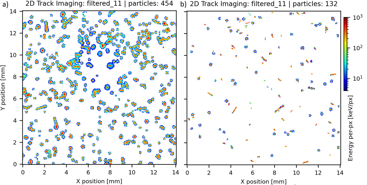
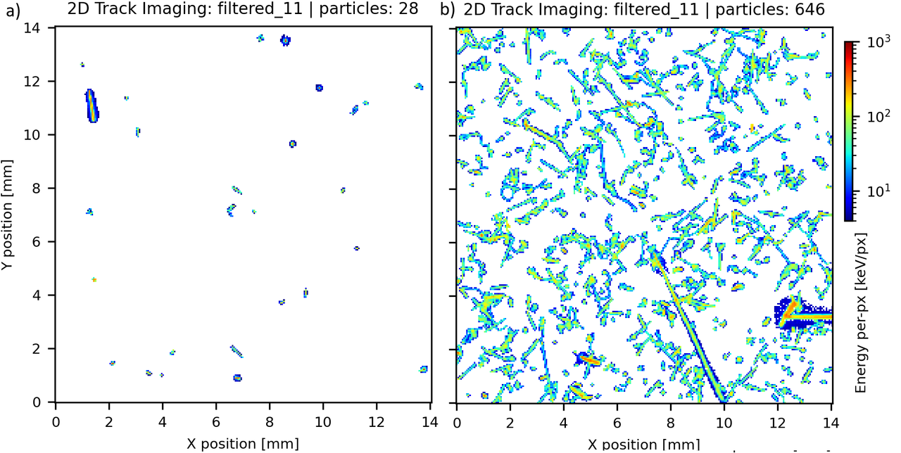
Gallium arsenide (GaAs) has been extensively studied for over seven decades as an excellent material for semiconductor lasers, LEDs, and microwave electronics. GaAs also offers significant advantages over Si and Cd(Zn)Te for radiation detector applications. In particular, GaAs exhibits higher electron mobility than both Si and Cd(Zn)Te, a higher average atomic number than Si, and a lower probability and energy of fluorescence photons compared to Cd(Zn)Te. These properties result in fast charge collection and improved signal uniformity compared to Cd(Zn)Te. High absorption efficiency up to 80 keV is required in medical computed tomography (CT) and security imaging, which can be achieved using 2 mm thick GaAs sensors. Additional applications of GaAs include mammography, small-animal imaging, electron microscopy, synchrotron radiation facilities, X-ray free-electron lasers, and non-destructive testing.
Advafab has developed a chromium-compensation process for commercially available 3-inch n-type GaAs wafers to produce high-resistivity and high-flux-tolerant GaAs sensors. In this process, wafers are annealed in a quartz reactor, followed by lapping, polishing, lithographic patterning, metallization, and dicing. Previously, we demonstrated wafer-level processing of 500 µm thick GaAs sensors using designs compatible with various readout ASICs. More recently, we have succeeded in the fabrication of thicker GaAs sensors, up to 2 mm thickness, to match the absorption efficiency of 750 µm thick Cd(Zn)Te sensors. The high-resistivity GaAs sensor wafers with thicknesses of 0.6, 1, 1.5, and 2 mm were fabricated. Each wafer contains Medipix-type 55 µm pitch and large-pixel sensors with approximately 330 µm pitch. The Medipix-type sensors were flip-chip bonded to Timepix3 (TPX3) ASICs and delivered for evaluation
Fine-pitch TPX3 sensor modules are particularly well suited for studying the details of the sensor material properties, such as count-rate uniformity, charge sharing, and spatial and energy resolutions. As the sensor thickness increases, sidewall finishing becomes increasingly critical and can strongly influence the count rate near sensor edges. We have demonstrated that sidewall etching after dicing significantly improves sidewall resistivity and electric field distribution near the sensor edges. The detailed fine-pitch imaging evaluation results will be presented.
High photon-flux operation was evaluated using a medical CT X-ray tube in an open-beam configuration. The 2 mm thick GaAs sensors with a 330 µm pitch tolerate and operate stably in extreme X-ray fluxes of up to 1.100 Mcnt/s/mm$^2$.
In conclusion, the presentation demonstrates the feasibility of manufacturing chromium-compensated GaAs radiation sensors of different thicknesses for photon-counting applications, achieving high uniformity and stable operation capability under high X-ray flux conditions.
Gain in silicon, and possibly SiC, detectors enables real 4D tracking. It is usually achieved with LGAD doping profiles, and is now also being explored in CMOS projects such as CASSIA and ARCADIA. This work studies whether sufficient electric field, and therefore gain in 3D detectors, can be generated by field focusing rather than doping.
The sensors were fabricated on the 8-inch CMOS process platform at the Institute of Microelectronics of the Chinese Academy of Sciences (IMECAS). They achieve an aspect ratio of 70:1 with an electrode width of 0.5 μm. Unlike a traditional 3D pixel sensor with columnar anodes, the columnar cathode is surrounded by a deeply etched trench. The trench shape can be square or circular, and both versions were studied. The sensitive layer is a 30 μm high-resistivity p-type epitaxial layer grown on a low-resistivity p-type substrate. Both the enclosed 3D-Trench anode and the central columnar cathode are etched from the front side. The 3D-Trench anode fully penetrates the epitaxial layer and extends 5 μm into the substrate, while the central columnar cathode stops 5 to 10 μm above the substrate.
Measurements with 2PA- and 3PA-TCT on irradiated and non-irradiated devices show no typical breakdown at the electrode tip. Instead, only a modest charge increase with depth is observed, likely due to self-quenching caused by the high density of multiplied holes at the tip, where hole impact ionization dominates. This suggests that, unlike other 3D sensors such as FBK and CNM, breakdown does not occur at the tip but along the column. The results indicate that below certain central-electrode radii, breakdown is suppressed at the tip, despite the highest electric field there, because the field is screened and breakdown shifts along the column. This could be a significant advantage over other 3D production; breakdown can be better controlled and maintained.
The presentation will show depth profiling of gain and breakdown dependence on the position of the TPA focal point and injected charge (changes in shape of the waveforms are recorded when approaching the breakdown point and maintaining its suppression in controlled way using fs-laser as probing tool).
Inverse Low-Gain Avalanche Diode (iLGAD) sensors developed at the Paul Scherrer Institute (PSI) in collaboration with Fondazione Bruno Kessler (FBK) have demonstrated an excellent Signal-to-Noise Ratio (SNR) and Quantum Efficiency (QE) in the soft X-ray range. In the current batch, single-photon detection is achievable at 400 eV with an SNR > 5 , while the QE surpasses 85% at 250 eV [1, 2]. Combined with the high frame rates of hybrid detectors, iLGAD-based hybrid detectors serve as an excellent candidate for time-resolved magnetic Small Angle X-ray Scattering (mSAXS) experiments in the soft X-ray energy range.
iLGAD sensors bump-bonded to 25 mm pitch charge-integrating MÖNCH chips were evaluated using a pulsed, ultrashort tabletop soft X-ray source [3] at the Max Born Institute (MBI). During the experiments, we measured highly monochromatized radiation between 700 eV and 1400 eV. These measurements were performed for two different iLGAD sensor designs, as well as for the standard sensor without gain layer. The influence of the sensor temperature on the gain was also studied throughout the measurements. Using the high-precision clock of the X-ray source, we were able to perform time-resolved measurements and optimise the timing parameters for the acquisition of the detector.
Finally, we successfully reproduced the mSAXS experiment with an FeGd superlattice sample, previously performed using a MÖNCH detector equipped with a standard silicon sensor [4]. Compared to the published report, the iLGAD sensors achieved a higher photon detection rate and, consequently, a higher quantum efficiency, particularly, for the lower-energy Fe L3-edge.

[1] A Liguori, et al., JINST 18 P12006 (2023)
[2] J Zhang, et al., JINST 17 C11011 (2022)
[3] M Borchert, et al., Rev. Sci. Instrum. 94, 063102 (2023)
[4] L Lunin, M Borchert, et al., Light Sci Appl 14, 394 (2025)
High-resolution X-ray spectroscopy is a cornerstone of modern research in astrophysics, fusion reactor diagnostics, and nuclear physics. For many decades dispersive crystal spectrometers have been the technology of choice, offering exceptional energy resolution. However, their narrow bandwidth and lack of imaging capabilities, as well as their cumbersome setups limit their applicability. Superconducting microcalorimeters, particularly Transition Edge Sensors (TES), have emerged as a transformative alternative technology. TES are non-dispersive single photon detectors that combine broad-band sensitivity, exquisite energy resolution, and imaging capabilities when combined with optics. Their properties can be tuned such that they can be made suitable for photon energies ranging from the far-IR to gamma-rays. Advances in their fabrication now enable the production of highly uniform arrays comprising thousands of TES detectors, opening new frontiers in X-ray spectroscopy [1].
This talk will provide an overview of TES-based X-ray spectrometers, covering their operational principles, state-of-the-art readout technologies (with a focus on Frequency Domain Multiplexing, FDM), and performance benchmarks. We highlight their potential, such as energy resolutions better than 3 eV for photons with energies ranging from 0.2 to 10 keV with high detection efficiency, as well as the technological challenges associated with their usage.
Two flagship applications will be highlighted: the X-IFU instrument on ESA’s New-Athena mission, designed to probe the hot and energetic universe with unprecedented imaging spectroscopic capabilities [2]. For this mission we are currently testing the performance and robustness of the Development Model. Secondly, we discuss the TES-EBIT instrument, a system in which our TES-FDM spectrometer is combined with an Electron Beam Ion Trap (EBIT). This instrument enables us to study with ultra-high-precision a large variety of highly charged ions for the support of current and future space-born X-ray observatories as well as fundamental nuclear physics.
[1] L. Gottardi et al., Appl. Sci. (2021), 11(9), 3793
[2] P. Peille et al., Exp. Astron. (2025), 59(2), 18
The authors acknowledge funding from the European Union’s Horizon 2020 Programme under the AHEAD2020 project (grant agreement n. 871158 and n. 654215) and the European Space Agency through ESA CTP underGrant 4000130346/20/NL/BW/os and in part byNWO, The Dutch Research Council through SRON.
We report the first characterization results of an optical time-stamping camera based on the Timepix4 chip coupled to a fully depleted optical silicon sensor, enabling sub nanosecond scale, time-resolved imaging down to the single-photon level. The characterization has been performed in direct detection mode, with a fast image intensifier for optical photons, and using a high-gain microchannel plate (MCP) and fast scintillator for electron and ion detection.
An RMS time resolution of 0.3 ns is achieved with photons in direct detection mode without the intensifier, from 0.6 to 1.5 ns in the single photon regime with an intensifier, depending on different amplitude-based signal selections, and reaching 0.5 to 1.3 ns when using a high-gain MCP. These results demonstrate a significant improvement over previous Timepix3-based cameras in terms of timing precision, as well as pixel count and data throughput.
We analyze key factors affecting performance, including sensor bias and timewalk effects, and demonstrate effective correction methods to recover high temporal accuracy. In addition, the potential of Low-Gain Avalanche Diode (LGAD) sensors is also explored as a promising route toward further enhancement of signal gain and timing performance.
Thanks to its excellent temporal resolution, event-driven readout, and high-rate capability, the systém represents a scalable platform for a wide range of applications, including quantum optics, ultrafast imaging, time-correlated photon counting, and mass spectrometry.
Silicon Drift Detectors (SDD), thanks to their very small detector capacitance – and correspondingly low noise performance – represent the gold standard in X-ray spectrometry. In contexts where high detection speed is relevant, i.e. when the count rate is large, the area of the detector can be partitioned in an array of smaller SDD pixels. This allow to operate in parallel several readout channels, individually characterized by a typical upper limit of about 1 Mcps/channel (depending on the performance of the downstream digital pulse processor). Moreover, the reduced pixel area reduces the drift time as well. Monolithic arrays enable minimal dead area, as compared to tiling of separate detectors. In this contribution, we review the state of the art of the largest monolithic SDD arrays with reference to two ongoing projects (based on different readout concepts): the ARDESIA-64 a 64-pixel detector for synchrotron applications and the TRISTAN detector (166 pixels with integrated JFET) developed within the KATRIN neutrino experiment.
ARDESIA-64 is a monolithic array of 8 by 8 SDDs square pixels of 2.5-mm side (fabricated by FBK, Italy). This detector represents the evolution of the 16-channel antecedent [1]. To minimize the bonding parasitic capacitance, anodes are coupled to 4-channel low-noise CUBE charge sensitive amplifiers (CSA) glued on the back of the detector (Fig. 1). It has been developed for high-throughput X-ray fluorescence (XRF) experiments with synchrotron X-ray sources, such as XAFS and nano-mapping of the elemental composition of samples. Thanks to a maximum count rate of 1.5 Mcps per pixel (with suitable high-performance digital pulse processing), it is possible to target a total count rate of 100 Mcps, significantly reducing the scan time. In addition to the standard thickness of 450 m, a 1-mm-thick detector has been fabricated, targeting improved detection efficiency at higher energies (Fig. 2). One of the major challenges of densely pixelated monolithic detectors is charge sharing among adjacent pixels: it can be mitigated by means of mechanical (Fig. 3) or electronic collimation [2], offering higher efficiency.
When the density of pixels has to be pushed further, placing CMOS CSAs close to the anodes become impossible. A different approach can be adopted, recurring to the technology with anode-embedded JFET, that allows to place the readout electronics far from the detector. This is the case of the TRISTAN detector, fabricated by the HLL of MPP (Germany). It contains 166 hexagonal pixels of 3-mm equivalent diameter in 40 mm by 38 mm footprint [3]. Here the goal is to operate each channel at 100 kcps and tile 9 modules, in a 3 by 3 configuration for a total of 1494 pixels, in the focal plane of the KATRIN experiment for the search of hypothetical sterile neutrino [4]. Here the SDD is used to accurately measure the whole energy spectrum of electrons produced by the beta decay of Tritium. In conclusion, the potential for hyperspectral imaging with these detectors will be discussed.
Hybrid semiconductor detectors based on Timepix and Medipix family chips enable direct detection of ionizing radiation by converting incident particles into an electrical signal within the semiconductor sensor volume. This principle ensures high detection sensitivity while eliminating analog noise. These detectors combine a semiconductor sensor chip with a read-out chip (ROC), which provides signal processing, data acquisition control, and data transfer. The sensor chip is divided into a 256 × 256 matrix of individual pixels, each with a 55 μm pitch, providing high spatial resolution. Each pixel enables independent energy measurement, making these detectors highly flexible and precise imaging tools. Despite the excellent performance of existing detectors, it has been shown that technological modification of the ROC or sensor chip using an optimized laser ablation method can further expand their application potential.
This work focuses on the use of femtosecond laser ablation method, whose key advantage lies in minimal thermal impact on the material and limited damage to the crystal lattice, enabling precise modification of detector structures without degrading their functional properties. The method was tested for 3D shaping of the ROC on a MiniPIX TPX3 detector with a CdTe sensor (1 mm thick), as well as for edge shaping of silicon sensors. Using the optimized laser ablation process, the ROC was thinned to a minimal thickness while maintaining full detector functionality. Such a modified ROC enables back-side illumination, significantly reducing X-ray attenuation. Experimental results demonstrate that this configuration allows efficient detection of low-energy photons (5–25 keV), which is significantly limited under standard front-side illumination. At the same time, an improvement in spectroscopic performance was observed, particularly a reduction in charge losses during transport and an increase in spatial resolution.
In addition to ROC shaping, laser ablation method was also applied to silicon sensors, specifically for precise edge cutting. Optimization of this process enabled reduction of the inactive region of the Si sensor without negatively affecting the response of edge pixels. This approach allows efficient tiling of individual processed Si modules into large-area detection systems (so-called monolithic assemblies) without loss of functionality. These findings will be further utilized in the development of advanced detection systems.
The authors acknowledge funding from the Technological Agency of the Czech Republic within the grant FW10010210 "Sensor Chip and Technology for X-ray Imaging".
Grab a coffee, and meet your colleagues in the Foyer
JUNGFRAU is a charge-integrating hybrid pixel detector developed for applications at the X-ray free electron lasers (XFELs, e.g. SwissFEL) and further extended to synchrotron use. With a dynamic range of $10^4$ 12.4 keV photons per pixel per frame, JUNGFRAU has enabled advances in many fields of photon science. However, increased brilliance due to recent upgrades at many synchrotrons and very high intensity applications at XFEL facilities poses an additional challenge for the detector due to pixels saturation. Additional developments to the detector are required to make use of those very high intensities.
As synchrotrons and XFELs have different beam delivery schemes, two different approaches for a dynamic range extension were developed. Synchrotrons typically deliver bunches over the full charge integration window at high repetition rates. For those applications, additional circuits were implemented in the ASIC to evaluate the state of each pixel in the array and predict which pixels will saturate before the integration ends. For saturated pixels, the new value can be linearly extrapolated under a quasi-continuous beam assumption (defined as beam intensity changes slower than 1 / frame rate). This approach allows the dynamic range to be extended by almost a factor of 10. XFELs, on the other hand, deliver very fast, brilliant pulses at much slower repetition rates. In this case, all the charge is deposited in the detector instantaneously at a given time (usually towards the beginning) in the integration window. So, for these applications, a dedicated ASIC was developed whose circuits implement an additional frontend gain configuration which avoids saturation at higher photon flux, extending the dynamic range by a factor >3x.
In this contribution, we present a performance evaluation for both the above-mentioned approaches obtained from table-top laser measurements and an experiment with X-rays beam at the SwissFEL Cristallina endstation.
Hybrid pixel detectors traditionally separate sensing from advanced signal processing, constraining pixel-level functionality to analog conditioning and threshold-based interpretation [1,2]. Our earlier work [3] introduced the concept of embedding artificial neural networks (ANNs) directly within pixels to enable local inference and mitigate the impact of analog non-idealities such as noise, gain non-linearity, and baseline offsets. Building on this idea, we then demonstrated [4] an in-pixel ANN architecture designed for pulse amplitude reconstruction, improving photon energy estimation from digitized signals.
In this work, we extend this concept by demonstrating post-fabrication functional reconfiguration of the in-pixel neural network. We show that a fabricated pixelated readout ASIC, originally designed and optimized for pulse amplitude (photon energy) estimation, can be re-trained to perform time-of-arrival (ToA) estimation without any modification to the underlying hardware. Each pixel contains a compact ANN with four hidden layers and a total of over 400 trainable weights, which processes the ADC-digitized pixel signal locally. By updating only the network parameters and processor instructions, the same in-pixel network can be repurposed to perform a fundamentally different measurement task.
We present experimental results of this re-training process, demonstrating accurate ToA estimation directly at the pixel level. Modifications to the network parameters, processor instructions, and the associated test and measurement setup [5] are described. These results demonstrate the capability of pixels with embedded neural networks to be flexibly reconfigured and dedicated to various application-specific measurement tasks.
Resistive Micromega detectors have demonstrated excellent performance, making them strong candidates for future collider experiments. In this context, we investigate a novel readout concept based on capacitive charge sharing, aimed at improving spatial resolution while significantly reducing the number of electronic channels. Such an approach is especially attractive for experiments characterized by moderate to low particle rates, such as FCC-ee, where good spatial resolution, long-term stability, simplicity of implementation, and cost-effectiveness are key requirements.
The detector architecture employs resistive layers coupled to a multi-layer capacitive readout structure. The induced signal is distributed across several layers of pads with decreasing granularity, where only the last layer—featuring larger pads—is instrumented for readout. This configuration enables controlled charge sharing among neighbouring channels, allowing precise position reconstruction through charge interpolation. The scalability of the concept is demonstrated by the successful construction of large-area prototypes with active dimensions of 40 × 50 cm².
We present results from beam tests performed with these prototype detectors, focusing on spatial resolution, efficiency, and rate capability. The studies were carried out using detectors featuring different numbers of capacitive sharing layers and various readout geometries, allowing a detailed assessment of the impact of the readout configuration on detector performance.
The results demonstrate that capacitive charge sharing in resistive Micromegas provides a promising and scalable path toward high-precision, large-area tracking detectors for next-generation collider experiments.
Grab some lunch and coffee
This talk explores Siemens Healthineers’ journey in the development of the first clinical photon-counting computed tomography (CT) systems. Originating from detector technologies in particle physics, the translation of photon-counting principles into real-world medical imaging has required overcoming a series of technological and clinical challenges. Along this path, numerous milestones have been achieved, accompanied by valuable insights into system design, integration, and clinical applicability.
In this presentation, we will highlight key challenges encountered during this transition and provide insights into the strategies and innovations that enabled their successful resolution. Particular emphasis will be placed on the interplay between detector physics, system engineering, and clinical requirements.
To illustrate the real-world impact of this technology, we will present a motivating example demonstrating how photon-counting CT is already improving the lives of patients, their families, and healthcare systems.
Finally, the talk will conclude with a forward-looking perspective, exploring future directions and potential breakthroughs in photon-counting CT technology, and outlining how this innovation may continue to shape the next generations of medical imaging.
The LCLS‑II X‑ray free‑electron laser facility is set to deliver an unprecedented repetition rate of up to 1 MHz, enabling novel scientific and discovery capabilities. Fully harnessing these capabilities requires imaging detector systems and data acquisition (DAQ) to sample and process data at correspondingly high frame rates. The ePixUHR family of detectors targets continuous acquisition of megapixel images at 35 kHz, while the future SparkPix family is designed to achieve MHz rates [1]. In this context, on‑detector calibration opens a path for machine‑learning workflows to be executed directly at the detector level.
In serial crystallography experiments, protein crystals are suspended in a stream of supporting liquid that is continuously intercepted by the X‑ray beam [2]. When a crystal is hit, it produces a diffraction pattern of interest; however, fluctuations in X‑ray pulse power and diffraction from the liquid support make discrimination between hits and misses a complex classification task. Discarding images with no diffraction pattern would provide a sizable reduction in storage and computing requirements, helping pave the way toward future MHz‑rate systems. An ePixUHR camera consists of multiple modules, each composed of six ePixUHR ASICs arranged in a 3×2 pattern and an acquisition FPGA. Because the full camera image is assembled later in the DAQ system, classification models must be designed with this natural segmentation in mind.
In this work, we present the design and characterization of a complete serial‑crystallography edge‑ML online classification pipeline. We follow the approach described in [2], with special attention on developing preprocessing methods that can be efficiently deployed to an FPGA. On‑detector calibrated sub‑images from each module are normalized, downsampled, stitched and then fed into a CNN‑based model, which is deployed on the DAQ FPGAs using the SLAC Neural Network Library [3]. The neural network produces an embedding vector that is passed to the DAQ; embeddings from the detector modules are then combined to produce a hit/maybe/miss classification, following the approach in [2]. The system has been deployed to a Varium C1100 evaluation card, where it utilizes less than 30% of the available configurable logic blocks, and less than 5% of the digital signal processors. The firmware was then validated using data from [2] whose geometry was adapted to match the one of ePixUHR 4-megapixel. Matching with software was in the order of 32-bit floating point machine precision. Frame rates in excess of 43 kHz could be sustained. We will also describe validation measurements of the detector performed as part of this effort.
References
[1] H. Sandberg et al., 2025 JINST 20 P08019
[2] T.-W. Ke et al., (2018). J. Synchrotron Rad. 25, 655-670.
[3] R. Herbst et a., Springer, pp. 120–134, 2022
Acknowledgements
R&D at the Linac Coherent Light Source (LCLS), SLAC National Accelerator Laboratory, is supported by the U.S. Department of Energy, Office of Science, Office of Basic Energy Sciences under Contract No. DE-AC02-76SF00515
The MÖNCH detector [1],a charge-integrating hybrid pixel detector with a 25 μm pixel pitch, has achieved micrometer-scale spatial resolution [2] by exploiting the charge-sharing effect via the analytical interpolation [3], enabling photon-starved applications at third-generation synchrotrons and lab X-ray sources. However, the applicability of conventional interpolation algorithms is limited to low photon fluxes (~$10^5$ ph/s/mm2), as they require spatially isolated single-photon events, thereby limiting experimental efficiency and hindering deployment at high-brightness fourth-generation synchrotrons.
With the goal of improving the spatial resolution and the flux operating range, a deep learning (DL)-based framework for sub-pixel localization of single and pile-up X-ray events has been developed. High-fidelity simulations [4] provide comprehensive training dataset. For single-photon events, the DL model achieves a spatial resolution of 1.8 μm, representing a 24% improvement over conventional interpolation (Figure 1). We attribute this improvement to the model’s ability to capture absorption-depth-dependent charge-sharing profiles, rather than relying on a single, depth-averaged analytical distribution. Furthermore, the proposed approach enables, for the first time, the reconstruction of two-photon pile-up events with 5.0 μm spatial resolution (Figure 2), thereby extending the operational flux range of MÖNCH by a factor of ~ 2 while preserving sub-pixel position sensitivity.

Figure 1. (a) Siemens star resolution target imaged under low-flux conditions and reconstructed using the proposed deep learning framework. (b) Normalized edge-spread function and a fitted Error function with a sigma of 1.8 μm.

Figure 2. Two-photon pile-up reconstruction from high-flux Siemens star measurements. (a) Accumulated pile-up events. (b) Deep learning-based sub-pixel reconstruction.
In this contribution, we detail the DL architecture, training strategy, and quantitative performance benchmarks compared to conventional interpolation. We also discuss the extension of this framework to polychromatic pile-up events, along with preliminary results.
[1] M. Ramilli et al 2017 JINST 12 C01071
[2] S Cartier et al 2014 JINST 9 C05027
[3] E. Belau et al., Nucl. Instrum. Methods Phys. Res. 214 (1983) 253–260
[4] X. Xie et al 2026 NIMA 1081 170894
Advances in CZT detector technology continue to improve performance in gamma ray imaging, yet achieving high spatial resolution by reducing pixel size rapidly increases readout channel count, system complexity and cost. SPECT systems are a key example of a technology that would benefit from reduced pixel size. Current systems use 2–2.5 mm pixels [1], but emerging clinical demands, including faster scans, lower dose and improved spectral separation require enhanced, ideally 3D, position resolution.
High-resolution subpixel positioning and depth-of-interaction (DOI) estimation is achieved without requiring cathode signals through a machine learning model trained on high precision simulated datasets. The final adjustment between the simulation model and the real data is done using a comparison between a few key performance parameters [2]. This removes the need for extensive calibration procedures and supports scalability to large-area CZT detector arrays.
The method has been applied to a CZT camera [3] comprising 5 mm thick quad modules, each with an 11×11 array of 2 mm pixels. The latest machine learning model enables per-pixel performance and supports up to 10×10 subpixelisation (as shown in Figure 1), achieving ~250 µm spatial resolution, with corresponding DOI resolution of ~1 mm near the cathode surface and ~500 µm at mid-depth. An energy correction is also applied which compensates for DOI-dependent variations and charge sharing losses, significantly reducing low-energy spectral tailing.
Recent work has focused on improving image uniformity and robustness to operational fluctuations by incorporating these effects into the training process and refining model regularisation. However, despite this progress, a key limitation of this approach remains the increased demand on readout speed and bandwidth. The model’s positional accuracy relies on the acquisition of both positive and negative signals across clusters of pixels associated with each interaction, significantly increasing data volume and processing requirements. These constraints present a challenge for real-time operation and system scalability.
To address these challenges, we explore the integration of neural network processing directly within a compact system-in-package (SiP) platform at the detector front-end, enabling on-the-fly photon-by-photon signal processing [4,5].
This approach enables early interpretation of time-varying detector signals, allowing the system to output only high-level interaction information rather than raw waveform data. The signal chain incorporates a dedicated ASIC that routes electrode signals through discrimination and digitisation stages, with sampled data stored in synchronised cyclic buffers. Upon event detection, buffered signals are processed by a neural-state machine, where a neural network performs detailed signal analysis and event characterisation.
A dedicated detector signal simulation framework is being developed to support this architecture. Building on previous subpixelisation training models, it incorporates realistic pulse-level signal generation in COMSOL Multiphysics (as shown in Figure 2), enabling direct simulation of digitised detector outputs and providing a controlled environment for training and validating neural network architectures for front-end implementation.
Direct pulse shape processing is expected to improve identification and discrimination of multiple interactions within the detector compared with conventional systems based on pulse height measurements from shaping amplifier circuitry. The first implementation of this framework will be presented, together with initial results demonstrating improved event discrimination and multi-interaction event reconstruction.
These developments enable a new class of high-resolution gamma detectors, combining improved speed and accuracy with reduced data volume and bandwidth requirements, with applications spanning medical imaging, industrial inspection, nuclear decommissioning and scientific space instrumentation [6].
[1] Matsunari I. Ann Nucl Cardiol, 10(1) (2019), 59–63.
[2] Kim JC et al. Nucl Instrum Methods A, 654(1) (2011), 233–243.
[3] Cherlin A et al. Proc. IEEE RTSD (2024).
[4] Kuvvetli I et al. Proc. IEEE RTSD (2025).
[5] DTU Orbit, https://orbit.dtu.dk/en/projects/i-rase-intelligent-radiation-sensor-readout-systems.
[6] Owe SRH et al. JINST, 19 (2024), C01005.
The authors acknowledge funding support from Horizon Europe (grant 101130550) and Innovate UK (grant 10037007).
The realization of large-area photon-counting X-ray detectors remains challenging due to the stringent requirements on charge transport and spectral performance. Although CdTe and CZT exhibit excellent energy-resolving capabilities, their implementation in large-area imaging systems is constrained by fabrication cost, scalability limitations, and spectral distortions associated with charge sharing and K-fluorescence escape 1. Amorphous selenium (a-Se) is particularly attractive for large-area applications because it combines direct X-ray conversion with mature deposition techniques. However, limited electron transport in a-Se results in significant charge trapping, leading to pulse-height degradation and reduced energy resolution 2. To address this limitation, a unipolar charge sensing detector (UCSD) architecture was evaluated as a means of minimizing electron-induced signal degradation. Experimental measurements were compared with GEANT4 simulations and analytical calculations to assess detector performance and establish consistency among the three approaches [3].
For the UCSD experimental setup, 135 V and 680 V are applied to the octagonal grid and top electrode, respectively, corresponding to an average electric field of approximately 8 V/μm. A 30 × 30 pixel binning scheme using 20 μm pixels is employed to reduce the input capacitance while preserving an adequate signal amplitude under low-signal conditions arising from the limited X-ray absorption efficiency of the 70 μm-thick a-Se sensor and the low activity (10 μCi) of the ²⁴¹Am source. For comparison, the same average electric field is applied to the conventional detector. The shaping times are set to 2 μs for the UCSD and 12 μs for the conventional detector. The same experimental configuration is implemented in both the simulation framework and the analytical model.
Figure 1 shows that the UCSD exhibits a significantly narrower photopeak and improved spectral response compared with the conventional detector in both the simulated and experimental spectra. The conventional detector shows substantial peak broadening and low-energy tailing due to incomplete charge collection associated with deep electron trapping, with FWHM values of approximately 24.2 keV and ~21.11 keV for the experimental and simulated spectra, respectively. In contrast, the UCSD reduces depth-dependent signal formation by decreasing the electron contribution to the induced signal, thereby preserving the spectral information more effectively. The FWHM energy resolution of the UCSD is approximately 8.3 keV and ~7.92 keV for the experimental and simulated spectra, respectively. The close agreement between the simulated and measured spectra indicates that the simulation framework successfully reproduces the dominant hole-transport and signal-formation mechanisms responsible for the improved detector performance.
Figure 2 presents the analytically calculated detector response under deep-trapping conditions. The analytical model is developed using charge induction and carrier-trapping formalisms adapted from previously reported charge collection efficiency models for photoconductive detectors [4]. A Gaussian
fitting is applied to estimate the FWHM values. The conventional detector exhibits a broad photopeak with an FWHM of approximately 22.4 keV, while the Gaussian-fitted photopeak width is 15.57 keV due to the strong low-energy tailing caused by deep electron trapping. In contrast, the UCSD demonstrates a significantly narrower photopeak with an FWHM of 7.88 keV. These analytical results predict a substantial improvement in energy resolution for the UCSD and further support the superior performance of the proposed detector architecture.
Overall, the UCSD structure improved the spectral performance of the detector by suppressing the electron contribution to signal formation. This improvement is supported by the good agreement between the experimental, Monte Carlo simulation, and analytical results. The remaining discrepancies between simulation, analytic and experimental results are likely associated with noise contributions, parameter uncertainties, and physical non-idealities that are not fully incorporated into the model, such as recombination, uncertainties in a-Se transport and trapping parameters, charge-cloud spreading, trap-filling effects, the assumed Fano factor, and Coulombic interactions between charge carriers.
1 S. O. Kasap, Photoconductivity and Photoconductive Materials. Wiley, 2022.
2 S. O. Kasap et al., J. Appl. Phys. 128 (2020), 124501.
[3] Y. Fang et al., Med. Phys. 39 (2012), 308–319.
[4] J. Stavro et al., J. Med. Imag. 5 (2018), 043502.
[5] A. Camlica, PhD thesis, University of Waterloo, 2019.
Spectral X-ray imaging based on single-photon-counting (SPC) detectors enables energy-resolved detection of individual X-ray photons, thereby offering substantial reductions in radiation dose together with improved tissue contrast, higher spatial resolution, and enhanced material decomposition capabilities in imaging modalities such as mammography and computed tomography (CT) [1]. However, achieving high spatial resolution remains a critical challenge in readout integrated circuit (ROIC) design [2]. To address this issue, we present, for the first time, the design and preliminary experimental results from a CMOS ROIC with frequency-division-multiplexed (FDM) readout [3] tailored for direct-conversion X-ray sensors such as amorphous selenium (a-Se) [4] and cadmium telluride (CdTe).
Use of FDM readout enables our ROIC, fabricated in a 1P6M 1.8-V-supply 180-nm CMOS process, to achieve a compact 50×50-mm2 pixel pitch without compromising count rate. Our novel approach relocates the analog-to-digital converter (ADC) in the SPC readout chain, which is normally located within the pixel, to a location outside the pixel array. This organization allows a single high-speed ADC to serve an entire column containing eight pixels, where the output from each pixel in the column is frequency-translated to one of seven carrier frequencies f1-f8, and then summed in the current domain and digitized by the column ADC.
As shown in Fig. 1, each pixel in a column consists of a charge-sensitive amplifier (CSA) followed by a CR-RC shaper which feeds a passive mixer. The mixer up-converts the shaped voltage pulse, which is then converted to a current Iout by a transconductance-amplifier (Gm) stage driving the column line. Output currents from each pixel Iout1-Iout8 are then summed before being converted back to a voltage by a transimpedance amplifier (TIA) and processed by an 8-bit 200-MS/s pipelined ADC.
As shown Fig. 2, experimental characterization of our fabricated ROIC prototype validates our proposed FDM-readout concept, demonstrating that independent photons from an Am241 source can be accurately isolated and reconstructed from the multiplexed data stream via digital down-conversion. In addition, our system achieves robust noise performance with an average equivalent noise charge (ENC) of 96 e- for a single pixel and 306 e- for the entire column (which includes eight pixels). Our shared column-parallel pipelined ADC achieves an effective number of bits (ENOB) of 7.3 bits and a peak signal-to-noise ratio (SNR) of 45.8 dB. Our ADC also exhibits excellent linearity with differential non-linearity (DNL) less than 0.5 LSB and integral non-linearity (INL) maintained within +/-1 LSB. Furthermore, the column-level TIA maintains a 200-MHz closed-loop bandwidth. Critically, our ROIC meets the high flux target count rate of 108 photons/(mm2×s), while adhering to a strict power budget of approximately 60 µW per pixel, which is essential to prevent a-Se sensor crystallization due to excessive heating [4]. These quantitative results establish FDM as a viable and scalable architecture for next-generation line-scanning SPC X-ray imagers.
Neutron radiography plays an important role in non-destructive evaluation, including aerospace inspection and battery analysis. Recent advances in compact accelerator-driven neutron sources and neutron flat-panel detectors (nFPDs) have improved the accessibility and performance of neutron imaging, enabling practical three-dimensional neutron computed tomography (CT). However, reducing acquisition time by decreasing projection numbers or exposure time, inevitably degrades reconstruction quality due to limited neutron statistics. This leads to a trade-off between measurement efficiency and image accuracy.
To address this issue, we proposed the Dykstra-like splitting with proximal minimization trick (DLPM) algorithm, which provides high reconstruction accuracy, fast convergence, and does not require empirically tuned parameters. Simulation results under low-dose CT conditions demonstrate that DLPM effectively suppresses noise compared to the conventional filtered back projection (FBP) method.
Furthermore, the proposed method is applied to industrial neutron CT using experimental data acquired at the compact neutron source AISTANS (AIST, Japan). The results demonstrate that DLPM is a practical reconstruction approach with potential for improving throughput in industrial neutron CT applications, particularly under time-constrained conditions.
Transmittance imaging enables the localization and mapping of various crystal features, such as defects and inclusions, within CdTe and CZT crystals [1]. By converting these identified locations into point clouds, we can analyse defect relationships using advanced computational tools, including neural networks. The resulting maps allow us to estimate crystal quality before the materials are processed and integrated into radiation detectors.
Charge collection properties can be verified using transient current measurements. By treating detector surfaces to allow laser pulse penetration, we can generate electron-hole pairs at depths determined by the laser's wavelength. Furthermore, by mounting samples on an XYZ-stage, specific internal regions of the detector can be systematically scanned [2-3].
When using a wavelength close to the bandgap, energy deposition from the laser pulse is continuous along its entire path. This inherent limitation of the Single Photon Absorption (SPA) technique can be overcome by utilizing ultra-fast laser pulses with a wavelength approximately double that of the bandgap. In this Two-Photon Absorption (TPA) technique, electron-hole pairs are generated within a much more confined volume inside the bulk.
In this contribution, we discuss the characterization of various CdTe crystals using transmittance imaging and transient current measurements. These detector materials are evaluated using both SPA and TPA techniques, performed with a standard TCT setup and the laser facility at ELI Beamlines in Dolní Břežany, Czechia.
[1] M Väänänen et al., J. Inst. 19 (2024), C12004
[2] M Bezak et al., J. Inst. 20 (2025), C01021
[2] M Bezak et al., J. Inst. 18 (2023), C02004
As the CMS pixel detector approaches the end of Run 3, it sustains increasing radiation damage that significantly impacts tracking performance. The resulting degradation in charge collection efficiency leads to "broken clusters" (pixels missing within a cluster) and "shorter clusters" (missing end pixels). These effects degrade track resolution and introduce substantial hit position bias, particularly in high-η regions where tracks traverse the silicon sensors at shallow angles. Figure 1 illustrates this effect: as the readout threshold increases relative to the diminished charge profile of an irradiated sensor, clusters progressively lose pixels and eventually split into fragments.

Figure 1: Charge loss after irradiation in a CMS pixel module. Top: schematic of a flipped module showing charge collection in the local y (global −z) and local x (global φ) directions. Bottom: cluster profile in z showing how increasing thresholds progressively break an irradiated cluster into fragments.
We present a novel, Alpaka-based [1] pixel "digi-morphing" algorithm designed for the CMS High-Level Trigger (HLT) to recombine these fragmented clusters. The algorithm operates directly at the individual pixel hit level using an image-morphing "closing" technique. It is a morphological operation consisting of a dilation step followed by an erosion step, each employing convolution kernels. The dilation expands cluster boundaries to bridge small gaps between fragments, while the subsequent erosion restores the cluster shape, retaining only the newly connected pixels. Figure 2 illustrates this procedure: a 3×3 kernel is applied to first dilate the broken cluster, filling in the gap, and then erode the result to recover the original cluster extent with the gap bridged.

Figure 2: Illustration of the morphological closing operation applied to a broken pixel cluster. A 3×3 dilation kernel expands the cluster boundaries (middle), and a subsequent erosion step (right) restores the shape while retaining the recovered pixels that bridge the gap.
While an offline version of the algorithm existed previously, the HLT deployment required a complete rewrite targeting the Alpaka portability framework to enable parallel execution on both CPUs and GPUs. The implementation supports regional morphing, allowing selective application to the most radiation-damaged detector regions which are currently the outermost module rings of the two first layers of the pixel barrel. Performance benchmarks demonstrate a negligible impact on HLT throughput with morphing enabled. Physics validation indicates a roughly 6.2% increase in average cluster size, confirming the successful recombination of fragmented hits without introducing spurious clusters in unaffected regions.
The current implementation employs two highly optimized packed 1-bit-per-pixel status buffers stored as a 1D array of 32-bit words, drastically reducing the memory footprint while maintaining algorithmic equivalence. A binary search over a sorted list of module identifiers is used to efficiently determine whether a given module should undergo morphing.
In this contribution, an explanation of the issue and algorithm will be presented, followed by a description of its implementation, and the study of its impact on performance and timing of local-reconstruction, as well as higher level track parameters.
The algorithm has been integrated into the CMS software framework (CMSSW) [2,3] and subsequently refined to fix the ongoing race conditions in edge case scenarios causing HLT crashes [4,5].
[1] E. Zenker, B. Worpitz, R. Widera, A. Huebl, G. Juckeland, A. Knüpfer, W.E. Nagel, and M. Bussmann, "Alpaka — an abstraction library for parallel kernel acceleration," 2016 IEEE International Parallel and Distributed Processing Symposium Workshops (IPDPSW), pp. 631–640 (2016)
[2] Digi Morphing for HLT, CMSSW PR #48734 (2025)
[3] Backport: Digi Morphing for HLT, CMSSW PR #48832 (2025)
[4] HLT digi morphing fix, CMSSW PR #49991 (2026)
[5] Backport: HLT digi morphing fix, CMSSW PR #50045 (2026)
The authors acknowledge the CMS Tracker DPG group and Andrea Bocci for contributions to the optimized implementation.
Alpha particles imaging with zero-dimensional halide perovskite scintillator
Chihaya Fujiwara1,2*, Yusuke Urano3, Akihiro Yamaji4, Akira Yoshiakwa1,2 and Shunsuke Kurosawa4,5
Real-time imaging of alpha-emitting radioactive dust is strongly required in decommissioning environments such as the Fukushima Daiichi Nuclear Power Plant in order to prevent internal exposure of workers. So far, detector systems combining scintillators with complementary metal–oxide–semiconductor (CMOS) image sensors have been developed [1,2]. However, conventional scintillators such as Ag:ZnS typically exhibit emission wavelengths around 400 nm, which do not match well with the peak quantum efficiency of CMOS sensors in the 500–700 nm range. This spectral mismatch significantly limits the detection efficiency and spatial resolution of alpha particle imaging. To achieve high-resolution imaging, it is essential not only to use scintillators with high light yield but also to tailor their emission wavelength to match the sensitivity range of CMOS sensors. Recently, zero-dimensional halide perovskite materials have emerged as promising scintillators due to their high light-output and tunable emission properties. Notably, their emission wavelength can be widely controlled from the blue to near-infrared region through compositional engineering. In this study, we focus on Cs2ZrCl6, a zero-dimensional halide material with high atmospheric stability, and investigate emission wavelength tuning via partial substitution of chlorine with iodine for alpha particles imaging applications.
Cs2ZrCl6 and iodine-substituted Cs2Zr(Cl,I)6 were synthesized by a melt-solidification at temperatures above 850°C. The obtained materials were ground into powders and mixed with an optical resin to fabricate composite scintillator imaging plates.
As shown in Fig.1 (a), under ultraviolet excitation, the Cs2Zr(Cl,I)6 composite plate exhibited intense yellow-to-orange emission, which was well matched to the high-sensitivity region of Si-based CMOS sensors. Using the fabricated imaging plate, clear visualization of alpha particle emitted from a ²⁴¹Am source was successfully demonstrated with high contrast as shown in Fig.1 (b). These results indicated that iodine-substituted Cs2ZrCl6 was a promising candidate for high-sensitivity and high-resolution alpha particle imaging.
[1] Y. Urano et al., J. Instrum., vol. 18, no. 12, p. C12009, Dec. 2023.
[2] S. Kurosawa, et al.,” J. Instrum., vol. 9, no. 07, pp. C07015–C07015, July 2014.
The push for higher photon fluxes needs to be countered by development of X-ray detectors capable of processing all these photon events. Presented is a custom made monolithic silicon drift detector (SDD), that has this goal in mind.
Besides discussing the design, preliminary performance results will be discussed.
The DSSC (DEPFET Sensor with Signal Compression) is a large-area, ultra-fast (4.5 MHz), soft X-ray (0.25 - 6 keV) camera developed for operation at the European X-ray Free Electron Laser. The pixel design features low-noise DEPFET technology with a modified doping profile that induces a signal-dependent gain, extending the detector's dynamic range. The full camera comprises 16 front-end modules, each containing 512$\times$128 hexagonal pixels of side length 136 $\mu$m, built on 725 $\mu$m high-resistivity depleted silicon. Previous studies of a single DSSC module have demonstrated low noise ($<$10 e$^{-}$) and high dynamic range (10$^{4}$). For future user operation, all 16 modules of the full 1-megapixel camera must be extensively characterised. Calibration data have been collected at the European XFEL to explore the full dynamic range of the DSSC for various gain configurations. Using PulXar, a laboratory X-ray source that mimics the timing structure of the European XFEL, the low-intensity, linear region of the detector response has been measured. For the high-intensity, non-linear region, the DSSC was installed at one of the European XFEL beamlines. Initial results show stable and uniform performance across all modules of the camera. Measurements of noise and gain are presented, and camera assembly, facility integration, and user operation are discussed.
The Timepix4 provides time of arrival (ToA) and time over threshold (ToT) information on detected events, enabling sub-pixel position reconstruction beyond simple pixel-centre assignment [1]. We present an evaluation of centroiding methods for Timepix4 electron clusters, aimed at improving spatial resolution by combining the complementary information carried by ToT and ToA. Using Allpix2 simulated data, we compare conventional ToT-weighted centroiding, ToA-based localisation, and a scaled-centroid approach designed to retain the sharpness of an anchor-pixel method, while recovering fractional position information from the cluster charge distribution.
The study investigates how the cluster ToT distribution can be used to estimate a physically motivated sub-pixel offset, based on the observation that the ToT-weighted centroid reflects the overall cluster shape, while the earliest ToA is often located close to the particle entry point and can therefore serve as an anchor for reconstruction. Several methods are explored to calculate this scaled centroid, including corrections derived from the displacement of the ToT-weighted centroid relative to the anchor pixel centre, and shape-dependent offsets informed by characteristic cluster topologies.
A comparison of the different centroiding strategies is performed on simulated datasets to assess their effect on sub-pixel hit distributions and imaging performance. The results show that pure ToT centroiding can introduce strong topology-dependent biases, while ToA anchoring preserves localisation near the point of entry but lacks fractional precision. The scaled-centroid approach provides a compromise between these two limits, maintaining proximity to the early-ToA anchor while introducing controlled sub-pixel shifts based on the cluster charge pattern. We discuss the physical interpretation of these methods and apply the centroiding approaches to 200 keV electron data acquired in a transmission electron microscope in order to study their impact on modulation transfer function and position reconstruction in electron imaging applications.
[1] N Dimova et al., NIMA 1075 (2025), 170335
In recent years, significant efforts have been undertaken to extend the operational range of hybrid photon-counting detectors towards the tender and soft X-ray regime. In parallel with the development of new sensor technologies — notably Low-Gain Avalanche Detectors (LGADs) and thin entrance windows (TEW) [1] — these efforts have focused on the optimization of readout ASICs, with the objectives of minimizing electronic noise and thus lowering the minimum detectable energy. In this context, DECTRIS has developed a prototype EIGER2 detector [2] tailored for tender X-ray detection using an experimental calibration with fluorescence targets down to silicon K-alpha (1.74 keV). The prototype was successfully tested at the SOLEIL Synchrotron, where it recorded its first synchrotron light, and is currently undergoing further testing and characterization. This contribution presents a subset of the characterization results obtained at SOLEIL over the energy range of 1–3 keV. The following figures of merit are addressed: Quantum Efficiency (QE), Detective Quantum Efficiency (DQE), Noise Power Spectrum (NPS), spatial homogeneity, spatial resolution as quantified by Modulation Transfer Function (MTF), and count rate performance, together with a determination of the minimum viable threshold setting.
[1] Baruffaldi, F., et al., Commun Phys 8 (2025), 321
[2] Donath, T., et al., J. Synchrotron Rad. 30 (2023), 723-738
The authors acknowledge the beamline teams of SIRIUS, METROLOGIE and MARS for allocating beamtime and their support.
Charge sharing constitutes a fundamental limitation in hybrid pixel detectors operating in single-photon-counting mode. As the charge cloud generated by an absorbed X-ray photon drifts toward the collection electrodes, it undergoes lateral diffusion. When the interaction occurs in proximity to pixel boundaries, the deposited charge is distributed among adjacent pixels. Consequently, instead of a single signal proportional to the photon energy being registered in one pixel, multiple reduced-amplitude signals are recorded in neighboring pixels, resulting in spectral distortion and degradation of energy resolution. A range of integrated circuit (IC) architectures has been proposed to mitigate charge-sharing effects [1–3]. These approaches differ primarily in the extent of interpixel communication, from schemes involving only nearest neighbors (e.g., four pixels) to those incorporating larger pixel clusters. However, increasing the number of participating pixels introduces important trade-offs, including increased analog noise and reduced count-rate capability—both critical parameters in high-flux imaging applications.
Furthermore, conventional X-ray imaging relies on time-integrated photon counting, where only the total number of detected photons is measured over a given acquisition period. In such measurements, individual photon interactions are neither spatially controlled nor resolved with respect to pixel boundaries, limiting the ability to directly observe and quantify charge-sharing phenomena. As a result, the spatial distribution of charge sharing can typically only be inferred indirectly. In this work, we present a detailed experimental characterization of charge-sharing distributions with subpixel resolution using a full-scale integrated circuit bump-bonded to silicon (Si) and cadmium telluride (CdTe) sensors of varying thicknesses. The measurements provide direct insight into the spatial behavior of charge sharing in pixelated detectors. The experimental results are systematically compared with theoretical models to assess their validity and to inform the optimization of interpixel communication algorithms for effective charge-sharing compensation.
This work is supported by the National Science Centre, Poland, project no. 2023/51/B/ST7/01782.
[1] A. Krzyzanowska, et al., Characterization of the Photon Counting CHASE Jr., Chip Built in a 40-nm CMOS Process With a Charge Sharing Correction Algorithm Using a Collimated X-Ray Beam, IEEE TNS. Vol. 64 (9), pp. 2561–2568, 2017.
[2] V. Sriskaran et al., High-rate, high-resolution single-photon X-ray imaging: Medipix4, 2024 JINST 19, P02024.
[3] M. Zoladz, et al. Tests of charge sharing compensation algorithm implemented in a single pixel counting integrated circuit operating with Si and CdTe pixel detectors, 2025 JINST 20, P12015.
Microchannel plates (MCP) are a kind of electron multiplier widely used for intensifiers, sensitive detection and time gated 2D imaging apparatus. With coating strips used as a photocathode, they become a powerful tool for X-ray detection [1]. In the Laser Megajoule Facility, they are key components to notably X-ray framing cameras embed in several plasma diagnostics (imagers of spectrometers DP1, DP3, DP9, DP10, and DP19).
For these time-resolved imaging systems to be reliable, we need to extensively characterize the time-response, spatial resolution and flux before saturation of the MCPs. Indeed, when used above nominal use MCPs can generate artifacts.
We will focus on three effects. A first effect concerns the intrinsic limitation of the time-resolution in the design: with a finite pulse duration, the electron multiplication gain continually drops while electrons transit in the channel, thus reducing the gain at short pulses. The second effect concerns cross talks between neighbouring channels which can lead to transverse artifacts up to nanoseconds after the signal [2]. Third, local saturation effects due to channel depletion can arise at high incident flux [3].
Most of these effects have possible parades [4]. We support our study with measurements made on MCPs from different manufacturers, either with picosecond pulsed UV light or continuous Xray irradiation.
[1] E. Kellogg et al, Rev.Sci Instr 47 (1976) 282
[2] L.R. Benedetti et al., Rev.Sci.Instr. 83,10E135 (2012)
[3] O.L. Landen et al., SPIE 0-8194-1251-1/93 (2002)
[4] L.R. Benedetti et al., Rev.Sci.Instr. 87,023511 (2016)
This work presents the characterization of a full detector module based on the DECTRIS JUNGFRAU charge-integrating ASIC, developed to overcome the count-rate limitations of traditional counting detectors [1]. The module consists of 8 ASICs in a 512✕1024 active pixel array, bump-bonded to a monolithic 450 µm Si sensor, for an approximate sensitive area of 4✕8 cm². The Jungfrau ASIC features a three-level dynamic gain-switching mechanism adjusting the gain frame-by-frame and pixel-by-pixel based on the incoming flux, which was derived from the Jungfrau ASIC, developed by the Paul Scherrer Institut (PSI) [2]. This capability allows for the simultaneous recording of intense diffraction peaks and low-intensity background, maintaining a dynamic range up to 12,000 photons per pixel at 12 keV, with single-photon sensitivity down to 6 keV. The ASIC supports continuous readout at frame rates up to 2 kHz.
Performance evaluations of the 8-chip architecture focus on electronic noise, linearity, and the consistency of the gain-switching mechanism across the full active area. Uniformity measurements of gain transitions, gain dispersion, and pedestal stability are included. A calibration concept for the multi-chip system using X-ray sources and internal charge injection is presented.
The development of a multi-module detector system is described, aiming for a 4M pixel configuration. Preliminary results of measurements at the DESY and ESRF synchrotrons are presented, validating the system performance under high photon flux, either continuous or instantaneous, for applications in serial crystallography [3,4]. Proof-of-concept measurements performed with the multi-module system will be displayed. Additionally, technical requirements concerning calibration, thermal stability, and data readout will be discussed. These results demonstrate the scalability of the DECTRIS JUNGFRAU for experiments at 4th-generation light sources.
References:
[1] Fröjdh et al., Front. Phys. 12 (2024): 1304896.
[2] Mozzanica, A., et al., Synchrotron Radiation News, 31(6), 2018.
[3] Orlans, J., et al., Commun. Chem., 8(1), 2025.
[4] Leonarski, F., et al., IUCrJ, 10(6), 2023.
The China Spallation Neutron Source (CSNS) is undergoing an upgrade to CSNS-II, targeting an increase in the proton beam power to 500 kW. This upgrade introduces stringent requirements for neutron detector readout electronics, including operation under vacuum conditions, higher neutron flux, increased counting rates, improved spatial resolution, and reduced power consumption. Conventional front-end readout systems based on discrete components suffer from high power dissipation and limited performance, making them unsuitable for future CSNS-II spectrometers.
To address these challenges, we have developed and experimentally characterized a prototype application-specific integrated circuit (ASIC), named HEROC (HElium-3 ReadOut Circuits), dedicated to position-sensitive Helium-3 tube neutron detectors. The ASIC provides an integrated, low-power analog front-end solution optimized for vacuum-compatible detector systems. Each channel integrates a charge-sensitive amplifier, pole-zero cancellation, shaping amplifier, and output buffer.
The fabricated HEROC prototype is an 8-channel ASIC and demonstrates an input dynamic range from 10 fC to 1.5 pC, with a counting rate of up to 500 kHz. Electrical measurements show an equivalent noise charge of 1130 electrons at an input capacitance of 15 pF, while the power consumption is less than 9.9 mW per channel, representing approximately a 90% reduction compared to the discrete-component front-end electronics previously used in the CSNS-I spectrometers. These characteristics make the ASIC suitable for high-rate and low-power neutron detection applications.
The ASIC was integrated into a prototype readout system including a data aggregation board equipped with an FPGA for data processing and a multi-channel ADC for signal digitization. Vacuum chamber measurements were performed to evaluate thermal behavior under vacuum conditions. After reaching stable operation, the ASIC temperature increased by less than 1 degree Celsius compared to operation in ambient air, indicating reliable performance with minimal thermal impact in vacuum environments.
Preliminary neutron beam tests were conducted at CSNS using two types of position-sensitive Helium-3 detectors with different geometries. Neutron charge spectra and time-of-flight distributions were successfully obtained. Using a slit collimator, the system achieved an optimal position resolution of 6 mm under nominal operating conditions. In addition, the ASIC-based readout system demonstrated stable operation with a counting rate of up to 125 kHz during the beam tests.
These results demonstrate that the HEROC ASIC effectively replaces traditional discrete-component front-end electronics, significantly reducing power consumption while enabling stable operation under vacuum and realistic neutron beam conditions. The ASIC-based readout system is a promising candidate for future implementation in CSNS-II spectrometer detectors, and further long-term beam tests are planned to fully evaluate its performance and stability.
Timepix detectors have a great advantage in the capability of spectral particle track imaging in um scale, reflecting the pixel size. This requires precise per pixel energetic calibration. The Timepix detector energetic calibration is achieved usually by photons with energies up to 100keV that create a charge in a single pixel, so-called low-energy calibration. High-energy heavy charged particles generate tracks across multiple pixels and the per pixel energy deposited into some pixels is often outside the low-energy calibration range leading to an underestimation of the measured particle energy. The principle of high-energy per pixel calibration of the Timepix2 detector with a Si 500 um sensor and Katherine readout was developed by the authors in [1] using MeV protons and Am-241 alpha particles and biasing the detector to 150V – 300V. However, the voltage applied to the Timepix detector affects the collecting electric field distribution and charge collection efficiency, which might affect the per pixel calibration.
This work focuses on the experimental investigation of charge collection by detecting protons of energies in the range of 0.1 - 1.6 MeV with Timepix2 detector with 500 um thick Si sensor and MiniPIX readout [2] depending on the applied bias in the range of 20-200 V. The proton energy spectra were compared with measurements of a single pad Si detector for precise calibration purposes. The measurements were performed at the Van de Graaff accelerator at IEAP CTU in Prague and supplemented with alpha particle measurements from Am-241 and U-233 Pu-238 Pu-239 triple source with energies from 4.8 to 5.5 MeV. The results have shown that the biasing of MiniPIX Timepix2 detector under 40 V causes incomplete charge collection and is inapplicable for spectrometry. With increasing biasing, the charge collection is complete, and spectral tracking of heavy charged particles can be done correctly with low-energy calibration up to certain particle energy. Further increase in bias causes signal distortion depending on particle energy and high-energy calibration must be used. The obtained results will help to avoid the need for complicated high-energy calibration by tuning appropriate bias in spectrometry of heavy charged particles of high energies. This will also be applicable for detecting fast neutrons, which produce heavy charged particles in the sensor when interacting.
[1] B. Bergmann et al., 2022 JINST 17 C01025
[2] C. Granja et al., 2022 JINST 17 C11014
Acknowledgement: This work was partially supported by grants APVV-22-0382 and DS-FR-24-0020 of the Slovak Research and Development Agency and funded by the EU NextGenerationEU through the Recovery and Resilience Plan for Slovakia under the project No. 09I05-03-V02-00073. Carlos Granja was affiliated at Advacam, Prague when the experimental measurements were performed.
This work presents a comparative study and optimization of a fast charge-sensitive amplifier (CSA) intended for hybrid pixel detectors operating in single-photon-counting (SPC) mode. The design objective is to minimize electronic noise while maximizing pulse-processing speed under stringent power constraints. Two advanced technology nodes are investigated: a 40 nm planar CMOS process and a 16 nm FinFET technology.
The CSA serves as the front-end stage of the readout chain and is optimized for low input capacitance typical of pixel detectors (~50 fF) and ultra-low power operation, with a bias current of approximately 5 µA. The core amplifier is designed to operate in the weak inversion (subthreshold) regime to maximize transconductance efficiency and achieve low-noise performance within limited power budgets. Particular emphasis is placed on the noise–speed trade-off and on the implementation of compensation techniques that ensure stable operation and fast pulse shaping across process variations and detector conditions.
Comprehensive simulations and performance analyses demonstrate that the FinFET-based implementation provides a significant improvement in pulse-processing speed compared to the planar CMOS counterpart, primarily due to superior electrostatic control and increased intrinsic device gain. Importantly, low-noise performance is preserved despite aggressive device scaling. These results highlight the strong potential of FinFET technology for next-generation high-rate photon-counting detectors, where both timing resolution and energy accuracy must be maintained under strict power constraints.
This work is supported by the National Science Centre, Poland, project no. 2023/51/B/ST7/01782.
The CoRDIA detector (Continuous Readout Digitising Imager Array) is an X-ray imager being developed for scientific experiments at diffraction-limited synchrotron rings.
It is designed to be capable of continuous operation at 150 kframe/s and features a compact pixel size (110x110 μm^2), that includes digitisation and fast data streamout circuits within the pixel array, so that they do not form blind areas [1].
The detector aims at being capable of single-photon discrimination capability at 12 keV, but is compatible with high-Z sensors for higher energy photons.
A charge-integrating, adaptive-gain circuit is used to extend its dynamic range to 1.75 kphoton/pixel/frame (~160 Mcount/pixel/s), and could be extended further in case of experiments having constant flux condition. It uses a pipelined architecture to achieve continuous Writing-Reading at the target rate.
Several test structure have been designed and tested to confirm expected performances in terms of response at the operational speed.
A larger (~20 kpixel) layout has been designed and is expected to be manufactured this year.
[1] A. Marras et al, 2024 JINST 19 C03006
The authors would like to acknowledge:
NIKHEF, for allowing to include a version of the PCS-GWT circuit in the CoRDIA design;
CERN, for allowing the reuse of CMOS IO pads and SOFIC ESD structures in the design;
Europractice, IMEC and CERN for their MPW and design tool support;
STFC, for the collaboration and cooperation.
The FAMU [1] experiment at RIKEN-RAL aims at a high-precision measurement of the hyperfine splitting of muonic hydrogen through the detection of an excess of characteristic X-rays emitted by muonic oxygen following laser-induced [2] excitation. The X-ray detection system is based on LaBr3:Ce scintillators read out by both photomultiplier tubes (PMTs) and SiPM arrays, requiring stable energy calibration over extended data taking periods.
SiPM-based detectors are known to exhibit gain variations correlated with temperature fluctuations and operating conditions, potentially degrading the energy resolution and affecting the stability of the reconstructed spectra. In this work, we present a calibration strategy based on the use of prompt X-ray flashes, intrinsically available during data taking, to monitor and correct gain drifts on a run-by-run basis. This method complements the standard offline calibration using radioactive sources and internal spectral lines.
The evolution of the detector response is studied over multiple data taking periods, showing residual gain variations at the percent level in absence of correction. The application of the prompt-based calibration allows for an effective stabilization of the energy scale and a significant improvement in the peak reconstruction consistency.
The resulting energy resolution is evaluated for SiPM-readout detectors and compared with that obtained using PMT-based systems. The performance is found to be competitive, with SiPM detectors achieving comparable or improved FWHM values in the energy range relevant for oxygen X-ray detection (~100–150 keV).
These results demonstrate the effectiveness of in-situ calibration using prompt signals for mitigating gain drifts in SiPM-based systems, representing a key element for stable long-term operation in high-rate X-ray spectroscopy experiments such as FAMU.
[1] Adamczak A., Bakalov D., Baldazzi G., Baruzzo M., Benocci R., Bertoni R., Bonesini M., Capra S., Cirrincione D., Clemenza M., Colace L., Danailov M., Danev P., Bari A.D., Vecchi C.D., Ferdinando D.D., Fasci E., Gaigher R., Gianfrani L., Hillier A.D., Ishida K., Lord J.S., Menegolli A., Mocchiutti E., Monzani S., Moretti L., Morgante G., Pizzolotto C., Pullia A., Pullia M., Ramponi R., Roman H.E., Rossella M., Rossini R., Sbrizzi A., Stoilov M., Suárez-Vargas J.J., Toci G., Tortora L., Vallazza E., Yokoyama K., Vacchi A., First operation of the FAMU experiment at the RIKEN-RAL high intensity muon beam facility, (2025) European Physical Journal A, 61 (12), art. no. 284, DOI: 10.1140/epja/s10050-025-01758-4
[2] Baruzzo M., Fasci E., Moretti L., Suárez-Vargas J.J., Cabrera H., Toci G., Capra S., Gianfrani L., Pizzolotto C., Mocchiutti E., Danailov M.B., Vacchi A., Long-term performance of a mid-IR laser system for muonic hydrogen spectroscopy in the FAMU experiment, (2026) Optics Communications, 608, art. no. 133082, DOI: 10.1016/j.optcom.2026.133082
With the High Luminosity LHC (HL-LHC) upgrade scheduled for 2030, a major upgrade of the LHCb experiment is planned to adapt to the harsh environment expected with the increased pile-up, as the number of interactions per bunch crossing will increase eight-fold. At the Upstream (UP) and MightyTracker tracking stations, Monolithic Active Pixel Sensors (MAPS) have been chosen for their high resistivity to radiation and their small pixel sizes. This high granularity and the higher particle density at HL-LHC will considerably inflate the data rate generated by these detectors. To fulfill LHCb’s design requirements, a data reduction method must be implemented directly at the sensor level.
In this work, we discuss the implementation of a demonstrator for an improved readout architecture with a lossless data format for pixel tracking detectors subject to high particle rates. This new architecture introduces a timestamp sharing stage, allowing our data format to remove the high redundancy of this information. Our data and readout simulations for UP in LHCb’s Upgrade II show that our method can achieve up to 36% compression rates compared to the best currently available solutions. This will allow us to meet the challenging data throughput conditions at UP in the Run 5 of LHCb, where particle rates can go up to 80 MHz/cm$^2$. The design can therefore allow for readout from 1 to 7 links, depending on the hitrate.
Our designed architecture prototype targets the LF150 technology node for submission in June 2026. The chip, named BIG, for BxId Grouping, should respect the design requirements of UP. Its surface will be around 4 mm$^2$ with an optimized power usage for a datapath representing our complete architecture.
Portable 4π gamma-ray imagers are promising tools for nuclear security, decommissioning, and contamination monitoring. However, existing gamma-ray imagers are generally expensive, which limits their use in applications involving multiple imagers. One major reason for the high cost is that conventional systems require from hundreds to tens of thousands of readout channels, as well as complex processing of list-mode data including timing and energy information. Therefore, if a 4π gamma-ray imager based on a small number of detectors and simple signal processing can be realized, its cost can be significantly reduced.
In this study, we developed a compact 4π gamma-ray imager, the Coded Cube Camera for Gamma-ray (C3G), based on a small number of detectors and simple signal processing. C3G estimates the source direction using detector response patterns that vary with the incident gamma-ray direction, with detectors and lead shielding cubes arranged in a three-dimensional array. We previously reported a proof-of-concept prototype consisting of 8 detectors and 18 lead cubes in a 3×3×3 configuration [1]. In the present study, we extended this concept and designed and fabricated a practical system consisting of 24 detectors and 40 lead cubes arranged in a 4×4×4 configuration. HR-GAGG scintillators (10 mm×10 mm×10 mm) and silicon photomultipliers were used as detectors. The developed 24-detector C3G is shown on Fig. 1. The overall dimensions are 130 mm × 130 mm × 155 mm, and the total weight is 2.3 kg. A USB-C cable connected to a PC is used for both power supply and data transfer. C3G does not require coincidence detection and uses only the total counts recorded by each detector during the measurement time. It also uses far fewer detectors and readout channels than conventional gamma-ray imagers. C3G uses far fewer detectors and readout channels than conventional systems, and its cost is expected to be less than one-tenth that of conventional gamma-ray imagers.
Here, H denotes the measured detection intensity vector of the 24 detectors, R the response matrix of C3G for each gamma-ray incident direction, and W the unknown source distribution. Their relationship is expressed as H=RW. In this study, W was estimated by gradient descent to minimize σ=|H-RW|^2. The response matrix R was calculated by Monte Carlo simulation using GEANT4. 511 keV gamma rays were irradiated from a total of 614 directions defined by a 10° mesh in azimuth angle φ and polar angle θ, and the number of events with an energy deposit of 511 ± 34 keV was recorded as the detection intensity for each direction. These responses were then interpolated to a 5° mesh using spline interpolation, yielding a response matrix for a total of 2522 directions.
To experimentally evaluate the performance of the developed C3G, 11C (511 keV) produced with the AVF cyclotron at TIARA, QST, was used as the imaging target. First, in a single-source experiment, a 27 MBq 11C source was placed at φ = 180° and θ = 90°, approximately 120 cm from the C3G, and 60 consecutive measurements of 60 s each were performed, giving a total measurement time of 1 h. The reconstructed image obtained from the first 60 s measurement is shown in Fig. 2. The image was correctly reconstructed at φ = 180° and θ = 90°, and the full widths at half maximum of the line profiles in the φ and θ directions were both 5.9°. In addition, the summed intensity of the 3 × 3 pixels centered on the true source position decreased exponentially with time, and the half-life estimated from the fitted curve was 20.95 ± 0.51 min. This agrees well with the known half-life of 11C, 20.36 min, indicating that the C3G can track not only the source position but also the temporal change in radioactivity.
Next, a two-source separation experiment was performed using 28 MBq and 34 MBq 11C sources. The distance from the center of the two sources to the C3G was fixed at 100 cm, while the source-to-source distance varied to 60 cm, 40 cm, and 20 cm. Each condition was measured 300 s. When the source separation was 20 cm, the two sources could not be clearly resolved, and the minimum resolvable angular separation under this condition was found to be 23° (40 cm).
These results show that the developed 24-detector C3G realizes a low-cost compact 4π gamma-ray imager based on a small number of detectors and simple signal processing, and that its fundamental performance was confirmed through 11C imaging experiments. In future work, the target radionuclides will be expanded from below 200 keV to above 1 MeV to verify the effectiveness of this system as a low-cost 4π gamma-ray imager with a wide energy range and a wide field of view.
[1] Yoshiharu Kitayama et al., Jpn. J. Appl. Phys., 63, 076502, DOI:10.35848/1347-4065/ad5ba0, (2024)
To address the need for high-resolution muon imaging in environments with significant logistical constraints, we are developing a field-deployable detector system based on glass Resistive Plate Chambers (gRPCs). While RPCs are a mature and widely used technology, this work emphasizes the design of a gas-tight configuration suited for flexible muography applications. The system is conceived to meet key requirements such as compactness, mechanical robustness, operational autonomy, safety, and cost efficiency. Our RPC detectors are designed with various configurations, each featuring unique characteristics and performance attributes [1, 2].
This contribution presents the development of detectors carried out collaboratively across three institutes. It opens with a brief overview of the muography principles and motivations driving this work. It then provides an update on the current status of the detector development, highlighting recent advances in design, construction, and long-term performance evaluation as shown in Figure 1. [Figure 1: Efficiency Variations for three identical chambers over a span of ~18 month
[1] Kumar V et al 2024 Nucl. Inst. Met. A 1070 170025
[2] Ikram. S et al J. Appl. Phys., 138:174502, 2025
This work was partially supported by the EU Horizon Europe Innovation Action under grant agreement No. 101233379 (“KINETIKA”).
Highly compact and highly granular electromagnetic calorimeters are required for precision luminosity measurements at future e⁺e⁻ colliders. Such detectors are also essential for determining the positron multiplicity and energy spectra in the LUXE experiment [1], which investigates strong-field QED through laser–electron interactions.
In a luminometer, where Bhabha scattering serves as the gauge process, a compact sampling calorimeter with a small Molière radius enables a precise definition of the fiducial volume, improves the separation of electromagnetic showers from low-energy background, and reduces the required detector space. The proposed calorimeter design consists of alternating tungsten absorber plates and thin silicon detector layers. A similar design is needed to cover a large range of positron multiplicities the LUXE experiment. A partially instrumented multi-plane prototype with up to 11 silicon detector layers was tested in 1–6 GeV electron beams at the DESY II synchrotron. Each detector plane consists of a silicon pad sensor mounted on flexible Kapton circuits and supported by a lightweight carbon-fiber structure, enabling highly compact instrumentation with sub-millimeter thickness.
The detector planes were installed in 1.2 mm gaps between tungsten absorber plates corresponding to one radiation length each. Each plane consists of a 90 × 90 mm² silicon pad sensor segmented into a 16 × 16 matrix. The readout electronics, positioned outside of the stack, employs FLAME [2] ASICs integrating analogue front-end electronics and 10-bit ADCs.High-statistics data were collected to perform precise detector alignment and to investigate the longitudinal and transverse development of electromagnetic showers. Preliminary results on energy, position, and angular resolution, as well as measurements of the Molière radius and shower development, are presented. The current status of the prototype development and comparisons with simulation studies are also discussed .
[1]. Abramowicz, H., Almanza Soto, M. et al., Technical Design Report for the LUXE experiment., Eur. Phys. J. Spec. Top. 233, 1709–1974 (2024). https://doi.org/10.1140/epjs/s11734-024-01164-9
[2]. Mirosław Firlej et al 2026 JINST 21 P03005
The measurements leading to these results have been performed at the Test Beam Facility at DESY Hamburg (Germany), a member of the Helmholtz Association (HGF).
High-purity germanium detectors play a key role in rare-event searches performed in underground laboratories, where ultra-low electronic noise is essential to achieve the required sensitivity. In this context, charge-sensitive preamplifiers rely on very high-value feedback resistances (∼1 GΩ), whose implementation poses significant challenges in terms of integration, stability, and noise performance.
In this work, we present the development of a Giga-Ohm feedback resistor implemented in ASIC technology using a high-resistivity polysilicon layer. A major limitation of integrated high-value resistors is the additional noise induced by capacitive coupling to the silicon bulk substrate. To address this issue, we introduce a dedicated, selective bulk-etching process aimed at reducing parasitic capacitances and mitigating substrate-related noise contributions.
Experimental results obtained on fabricated prototypes are reported, with a detailed electrical characterization before and after the bulk etching procedure. These results represent a promising step toward the realization of low-noise integrated front-end electronics for next-generation rare-event experiments in underground environments.
SHINE (Shanghai HIgh repetitioN rate XFEL and Extreme light facility) is the first XFEL facility working in the hard X-ray region in China. To fulfill the special requirements of SHINE, a new pixel array detector, STARLIGHT (SemiconducTor Array detectoR with Large dynamIc ranGe and cHarge integrating readout), is being developed. HYLITE (High dYnamic range free electron Laser Imaging deTEctor)) is the front-end readout chip of STARLIGHT, which works in the charge-integration mode with a dynamic range of 1~10000 photons @ 12 keV. To enable such high speed, a 10-bit Analog-to-Digital Converter (ADC) is integrated into each pixel, ensuring that the pixel outputs are in digital format.
The HYLITE series is manufactured using a 130 nm CMOS process. The initial phase of HYLITE, HYLITE200F, was developed focusing on creating a 64×64-pixel chip with a 200-μm pixel pitch. The maximum frame rate of the first full-scale chip is 6.3 kHz in successive readout mode. The performances of the HYLITE200F chip are fully tested. The signal-to-noise ratio is 8.7, which indicates the ability for single-photon resolution. The 2×8-size front-end module has been manufactured to organize a single-module prototype detector system and has been adopted successfully on the SAXS end station of HEPS. Imaging tests show that the function of the module and the architecture of the detector are correct.
HYLITE100F is the second engineering run chip of HYLITE, aiming for a frame rate of 10 kHz. Compared with HYLITE200F, the pixel pitch of HYLITE100F is improved from 200 μm to 100 μm, while the maximum data rate is increased from 400 Mbps to 3.28 Gbps. The array size of the full-size chip is 128×128. In this architecture, two data ports are used for whole-chip data transmission. Each data port consists of a high-speed serializer, a low-speed serializer, and a CML (Current Mode Logic) driver. A clock management block was also integrated into the periphery of HYLITE100F to generate the necessary clocks, which consist of a PLL (Phase Lock Loop) and a frequency divider. The tests were carried out on a 16-ASIC test module without the sensor. An eye diagram analysis confirmed that the data port operates effectively at a data rate of 2 Gbps. The primary imaging tests showed that the function of the ASIC is correct. In this poster, we will introduce the design and test progress of the HYLITE series chips.
Silicon carbide (SiC) is a wide-bandgap semiconductor with significant potential for detecting various types of radiation. An additional advantage is the commercial availability of high-quality crystalline SiC materials necessary for the fabrication of radiation detectors. The 4H-SiC polytype is a good candidate because of a band gap energy of 3.23 eV at room temperature, a breakdown voltage of approximately 2 MV/cm, and a carrier saturation velocity of 2×10e7 cm/s. Due to these properties, SiC detector is a high-temperature, radiation-tolerant alternative to traditional silicon detectors. Current epitaxial growth methods can produce SiC layers thicker than 100 μm; however, for full depletion, about 1kV of reverse bias is needed. We have studied the influence of different metallizations on the electrical and detection properties of 4H-SiC detectors based on a high-quality epitaxial layers.
We have fabricated 4H-SiC detector structures based on a 100 um thick epitaxial layer grown on 4” 4H-SiC substrates. For detector preparation, the base wafer was cut into smaller parts. On the top (epitaxial layer) part, Schottky contacts were prepared using different metallizations. We utilized three types of elements (nickel, aluminium, and silver). The contact thickness was 50 nm with diameters of 1 and 2 mm. On the opposite detector side (base substrate), the whole area metallization based on Ti/Pt/Au was deposited. Prepared detector structures were placed in the shielded box, and current-voltage measurements were performed. The highest breakdown voltage was achieved with the standard Ni contact, to be of about 600 V. The lowest observable breakdown showed the detector structures with Ag contacts, which was at 400 V, while the highest leakage current ( up to10 nA) flows in detectors with Al contacts. In the case of Ag and Ni contacts, the leakage current was almost the same, and the value was in the range of 20 pA up to 40 pA. Radiation detection properties were tested using a triple alpha radiation source 238-Pu, 239-Pu, 244-Cm, which generated alpha particles with energies in the range from 5.1 MeV up to 5.8 MeV. The best obtained energy resolution of about 20 keV in FWHM (Full Width at Half Maximum) was observable for detectors with Ni contact. Also, structures with Al contact demonstrate high energy resolution, close to 20 keV, despite the highest leakage current. The worst energy resolution was observable in the case of Ag contact, which was surprisingly having the low leakage current comparable to Ni structures.
Acknowledgement: This work was partially supported by grants of the Slovak Research and Development Agency Nos. APVV-22-0382, SK-CZ-RD-21-0116 and funded by the EU NextGenerationEU through the Recovery and Resilience Plan for Slovakia under the project No. 09I05-03-V02-00073.
Rapid and reliable localization of radioactive sources is a critical requirement in nuclear security, border protection, radiological emergency response, and the prevention of illicit trafficking of radioactive materials. In our previous work, we investigated radioactive source position estimation using a coded aperture device combined with machine learning, demonstrating the potential of data-driven methods for directional radiation sensing [1]. Although coded-aperture systems can provide strong localization capability, they are generally more complex in design and reconstruction and may involve higher implementation cost. In the present work, we propose a simpler and more compact directional detector architecture intended for security applications, while retaining high angular localization performance.
The proposed system consists of three small-form-factor CZT detectors, each with a crystal volume of 0.5 cm³, arranged azimuthally at 120° with respect to each other. To enhance the directionality of the system, each detector is asymmetrically shielded using a lead cone placed around the crystal, together with a cylindrical lead endcap at the bottom (Figure 1). This shielding configuration modifies the angular response of each detector and enables the extraction of source-direction information from the relative count-rate pattern of the three-detector array. An important practical advantage of the system is that it operates without any moving parts, making it more robust, simpler, and potentially more suitable for field deployment in operational security scenarios.
The system was studied using GEANT4 [2] simulations. A 1mCi 137Cs source was placed at a distance of 50 m from the center of the detector system and simulated at azimuthal angles from 0° to 355° in steps of 5°. For each source position, the total counts recorded by each detector over a fixed acquisition time interval were used as the input features to the machine-learning model. A gradient-boosted decision tree model, configured with 100 trees, was developed within the KNIME analytics platform [3] and trained on the simulated dataset and subsequently evaluated on an independent validation dataset.
The results demonstrate that the proposed approach can determine the source direction with an angular accuracy of 2°, showing strong potential for practical directional radiation sensing. Owing to its compact design, lower complexity relative to coded-aperture approaches, and lack of moving components, the proposed system is particularly attractive for fixed-site monitoring, mobile security platforms, and rapid deployment in nuclear security applications. Experimental validation of the detector system is currently in progress.
[1]K. Karafasoulis, I. Kaissas, C. Papadimitropoulos, K. Potiriadis, C.P. Lambropoulos, “A machine learning approach in the estimation of a radioactive source position using a coded aperture device,” Journal of Instrumentation (JINST), 18, C01062, 2023.
[2]GEANT4 collaboration, GEANT4 — A Simulation Toolkit, Nucl. Instrum. Meth. A 506 (2003) 250
[3]M.R. Berthold, N. Cebron, F. Dill, T.R. Gabriel, T. Kötter, T. Meinl, P. Ohl, C. Sieb, K. Thiel, B. Wiswedel, “KNIME: The Konstanz Information Miner,” Studies in Classification, Data Analysis, and Knowledge Organization (GfKL 2007), Springer, 2007.
Report of the performance of the single‑sided silicon microstrip detector (MSD) used in the magnetic spectrometer of the FOOT (FragmentatiOn Of Target) experiment —devoted to fragmentation studies for hadrontherapy and space radiation protection— showing high (>95%) detection efficiency from recent beam tests at CNAO (National Center for Oncological Hadrontherapy, Pavia).
The paper presents an electronic thinning method for hybrid pixel detectors(HPD) used in electron microscopy. Theoretically, the spatial resolution of a pixel detector improves with decreasing pixel pitch. However, as the pixel size diminishes, a single incident particle may induce signals across multiple adjacent pixels caused by scattering, the charge-sharing effect makes it difficult to determine the actual point of particle entry.
To improve the spatial resolution of HPDs, some researchers have created super resolution techniques, such as Center-of-Gravity(CoG) method and position interpolation algorithms[1-2]. However, the results calculated by these methods often depart from the particle’s exact incident position because the algorithms are based on statistical distributions and the results are maximum likelihood estimates.
Although high-energy incident particles follow complex trajectories within the sensor layer, we noticed that the distribution of energy deposited by particles in the shallow layer of the incident surface is always highly correlated with the incident position. Energy deposited within the layer of interest can be filtered by a well-designed integration time window. This achieves an effect similar to the back grind of a monolithic active pixel sensor(MAPS), thus improving the spatial resolution of HPDs. Meanwhile, the design preserves the original amplitude of the detector signal in circuit, enhancing the signal-to-noise ratio and energy resolution for individual particles.
To validate this, we conducted Monte Carlo simulations using the standard simulation tool Allpix2. Considering the feasibility of subsequent experimental verification, we have developed a simulation model similar to EMPIX2[3]. By studying the patterns of energy deposition and induced current signals generated by 300 keV electrons in a 500 μm silicon sensor, we compared the spatial resolution before and after applying the electronic thinning method. The results indicate that electronic thinning method can effectively improve the position resolution of the detector; under certain conditions, position resolution as high as 54.69 μm (with a pixel size of 150 μm) can be achieved. We also verified the generality of this method by examining parameters such as pixel pitch and detector bias. In addition, algorithms have been developed to identify and handle events of wide-angle scattering. Future work will involve designing readout chips and constructing a test system based on these simulation results to conduct real-world experiments, while experiments using existing HPDs are also underway.
Figures are shown in attached pdf.
[1] Litwinek T et al, Journal of Instrumentation, 2025, 20(12): P12034.
[2] Ramilli M et al, Journal of Instrumentation, 2017, 12(01): C01071.
[3] Tong Wei et al, Journal of Instrumentation, 2023, 18(12): C12007.
Recent advancements in X-ray sources and experimental techniques have increased the demand for area detectors capable of covering a wide X-ray energy range, including the soft and tender X-ray regime, while supporting efficient data acquisition. In particular, low-energy X-ray measurements impose stringent requirements on detector noise performance, stability, and vacuum compatibility.
In this contribution, we present an evaluation of the XSPA series hybrid pixel array detectors with a focus on low-energy X-ray detection performance. The detector architecture is based on a readout design derived from the UFXC family of photon-counting ASICs [1] and is implemented in a vacuum-compatible housing suitable for soft X-ray experiments. Detector performance was evaluated using monochromatic X-ray measurements over a range of photon energies, focusing on energy response, noise separation, and operational robustness in the low-energy region.
Experimental results demonstrate that X-ray signals down to approximately 500 eV can be clearly observed and separated from electronic noise, confirming the applicability of the detector to soft X-ray measurements. Additional data obtained at higher photon energies further illustrate the linearity of the energy response and the stability of detector operation under practical experimental conditions. While detailed adjustment and optimization procedures are beyond the scope of this presentation, the results provide an overview of the achievable performance envelope in the low-energy regime.
The detector also supports high-throughput acquisition modes, including zero-dead-time operation and burst acquisition. Although such modes are not the primary focus of this contribution, they provide a flexible acquisition framework that can be combined with low-energy operation depending on experimental requirements.
The presentation will focus on experimental results and performance evaluation relevant to low-energy X-ray detection, with selected complementary measurements at higher X-ray energies performed to evaluate fundamental detector characteristics.
[1] P. Grybos et al., IEEE Trans. Nucl. Sci. 63 (2016), 1155–1161
The newly upgraded Swiss Light Source (SLS) 2.0, a fourth-generation synchrotron, has begun
operation. Photons with energies up to 80 keV will be available at increased flux compared to the
third-generation source it replaces. In particular, the brilliance is expected to increase by two orders of
magnitude. In this energy range, silicon is no longer an efficient detection material. High-Z
semiconductors are therefore required, with GaAs:Cr, CdTe, and CdZnTe (CZT) being promising
candidates.
Developed at PSI, JUNGFRAU is a charge-integrating ASIC designed to cope with the extremely
intense X-ray pulses from SwissFEL. Three gain levels, combined with dynamic per-pixel switching,
extend the dynamic range to 10⁴ photons at 12.4 keV in silicon. However, JUNGFRAU was designed for
hole-collection in silicon. In contrast, electron-collection is preferred in high-Z materials due to their
superior charge transport properties.
The dynamic range of JUNGFRAU in the highest gain mode (G0) has been optimized for
hole-collection, resulting in a linear dynamic range of ~330 keV, compared to electron-collection which
is limited to a linear dynamic range of ~110 keV. Methods are in development to better characterise and
improve the dynamic range performance. In this contribution, we will use these methods to investigate
techniques and detector configurations, aimed at extending the dynamic range of G0 in
electron-collection mode.
Diamond-based detectors have gained significant attention in fusion neutron diagnostics owing to their outstanding radiation hardness, sub-nanosecond timing response, and capability for energy-resolved measurements [1,2]. In this study, neutron spectrometry experiments were conducted at the KSTAR tokamak using two geometrically distinct single-crystal diamond detector systems. Time-resolved measurements of 2.45 MeV D–D fusion neutrons were performed during neutral beam injection (NBI) plasmas, with neutron emission rates reaching up to 10¹¹ n/s. The measured pulse-height spectra exhibited distinct signatures of the ¹²C(n,α)⁹Be reaction; the planar-type detector provided superior intrinsic energy resolution, whereas the axial-type detector achieved higher detection efficiency and operational robustness under high-flux conditions (>10⁸ n/cm²/s), making it more suitable for high-rate fusion environments [1,2]. A strong correlation with micro-fission chamber and ³He counter data verified the accuracy of neutron yield determination [3,4]. Owing to the inherently low gamma-ray sensitivity of diamond sensors, reliable neutron measurements were achieved even in mixed neutron–gamma radiation fields, highlighting their practical utility in realistic fusion reactor environments [2]. While the present work focuses on point-detection spectrometry, the demonstrated fast timing capability, high count-rate tolerance, compact form factor, and radiation hardness indicate that diamond detectors constitute a promising sensor platform for future fast-neutron imaging and tomographic diagnostics in fusion devices [1,5]. These results confirm the reliability of diamond detectors for real-time fusion neutron spectrometry and support their scalability for high-flux diagnostic applications foreseen in devices such as K-DEMO and ITER.
[1] C. Weiss et al., Fusion neutron diagnostics with CVD diamond detectors, Nuclear Instruments and Methods A (2024).
[2] C. Cazzaniga et al., Single-crystal diamond detector measurements of DD and DT fusion plasmas, Rev. Sci. Instrum. 85, 043506 (2014).
[3] Y. Lee et al., Diamond fast-neutron detector applied to the KSTAR tokamak, Fusion Engineering and Design 153 (2020) 111452.
[4] Y. Lee et al., D-D Fusion Neutron Spectrometer in the KSTAR Tokamak, Transactions of the Korean Nuclear Society Spring Meeting (2025).
[5] D. Rigamonti et al., Single-crystal diamond-based neutron diagnostics for fusion applications, Nucl. Fusion, 2024.
This research was supported by R&D Program of "High Performance Tokamak Plasma Research & Development (KFE-EN2601)” through the Korea Institute of Fusion Energy (KFE) funded by the Government funds, Republic of Korea.
Lead halide perovskites (such as CsPbX₃) have been highly spotlighted in the field of solar cells due to their outstanding optoelectronic properties, including excellent charge-carrier mobility and high stopping power.[1] Recently, leveraging these exceptional radiation-responsive characteristics, they have begun to be investigated as novel real-time dosimetric materials in the field of radiotherapy quality assurance (QA), which strictly requires high dosimetric accuracy. Accordingly, this study introduces chlorine-containing mixed-halide perovskites (CsPbX₂Cl) –materials not yet explored in the QA of high-dose-rate brachytherapy (HDR-BT), where the dose gradient changes drastically with distance–to evaluate their clinical feasibility. Notably, a commercial ion chamber (34013, PTW) was employed as a reference dosimeter for comparative evaluation.
The experiments were conducted using an ¹⁹²Ir source (~380 keV) embedded in a clinical HDR-BT system (Flexitron, Elekta). CsPbI₂Cl and CsPbBr₂Cl were selected to fabricate sensors using interdigitated electrodes (IDEs) with an active area of 0.5×0.4 cm² each. To evaluate their feasibility as QA dosimeters, the dose linearity over a range of 1-1000 cGy and the repeatability under 10 repeated irradiations of an identical dose were analyzed for the fabricated sensors and the reference ion chamber. The evaluation criteria were set to a coefficient of determination (R²) > 0.99 and a coefficient of variation (CV) < 1.5%.
The evaluation results demonstrated that all sensors, including the ion chamber, successfully satisfied the established clinical criteria. In the linearity assessment, the ion chamber exhibited R² = 0.9983, while CsPbI₂Cl and CsPbBr₂Cl sensors exhibited excellent dose proportionality with R² = 0.99864 and 0.99997, respectively, fulfilling the criterion. In the repeatability assessment, the ion chamber showed a CV of 0.875%, and the perovskite sensors showed highly stable signal reproducibility with CV values of 0.942% and 0.317%, respectively, proving their suitability as HDR-BT QA dosimeters.
Furthermore, the slope of the linearity graph and the mean Y-axis value of the repeatability graph indicate the sensor's response to the dose, serving as effective indicators of sensitivity. In both metrics, CsPbI₂Cl exhibited higher values, demonstrating superior sensitivity compared to CsPbBr₂Cl. These results are interpreted as the CsPbI₂Cl sensor exhibiting higher responsiveness to ¹⁹²Ir γ-rays due to its relatively higher effective atomic number (Z_eff) which elevates the photoelectric effect, whereas the CsPbBr₂Cl sensor demonstrated a more stable output (higher R² and lower CV) by suppressing background noise through its relatively wider bandgap.[2]
In conclusion, this study is highly significant as it confirms the clinical feasibility of Cl-containing perovskite materials, which have not been previously addressed in the HDR-BT QA field. Based on these findings, future research will focus on developing customized real-time dosimetry systems optimized for specific clinical purposes—such as high-sensitivity measurements or extreme stability—through halide compositional engineering, ultimately extending their application to actual patient QA environments.
[1] Yakunin, S., Sytnyk, M., Kriegner, D. et al. Detection of X-ray photons by solution-processed lead halide perovskites. Nature Photon 9, 444–449 (2015).
[2] Akkerman, Q. A., D’Innocenzo, V., Accornero, S. et al. Tuning the optical properties of cesium lead halide perovskite nanocrystals by anion exchange reactions. Nano Lett 15, 3691–3696 (2015).
This work was supported by a National Research Foundation of Korea (NRF) grants funded by the Korean government (RS-2025-16066841)
Particle discrimination is a valuable imaging detector capability for applications such as medical physics, environmental monitoring, decontamination, and nuclear forensics. Across these areas, samples can have complex matrices, and a large range of radioactivity levels, which present analysis and measurement challenges for digital autoradiography systems (e.g., knowing how long to measure and how to optimize acquisition parameters for different particle types a priori). Digital autoradiography with an ionizing-radiation Quantum Imaging Detector (iQID) records the location and time of individual scintillation events can overcome these challenges with real-time, enhanced particle discrimination capabilities.
The iQID is a scintillation-based imaging system that uses an image intensifier, lens, and a complementary metal-oxide- semiconductor (CMOS) camera. The iQID collects list mode data which contains information about the morphology of each individual scintillation flash. The list mode data is used to create images with various parameter cuts, such as event size, intensity, time, and shape. In its current operating modes, the detector can perform alpha or beta particle imaging which is mostly achieved by the choice of scintillator. Simultaneous dual particle imaging would streamline sample analysis, removing the need to swap scintillators and reducing measurement times.
A dual particle sensitive alpha/beta composite scintillator (ZnS:Ag with Gadox backing Qscint Imaging Solutions, LLC) was used to measure alpha and beta emitting sources separately to gather list mode data while maintaining all other acquisition parameters constant. Post processing focused on event cluster intensity, area, eccentricity to determine differences between alpha and beta scintillation events. A dual particle measurement took place where the alpha and beta emitting sources were physically separated and in post processing, the differences were utilized to determine whether each event was from an alpha source or a beta source. Leveraging the morphological differences in the scintillation events creates accurate radiological map in which multiple emission types can be represented from a single autoradiographic measurement.
The authors acknowledge funding from the following funding sources. This material is based upon work supported in part by the Consortium for Nuclear Forensics under Department of Energy, National Nuclear Security Administration award number DE-NA0004142. Kyle C. Hartig is supported in part by the Defense Threat Reduction Agency under the award number HDTRA1-20-2-0002. Ben McDonald and Hannah Patz are supported in part by the Pacific Northwest National Laboratory (PNNL) Laboratory Directed Research and Development Program Nuclear Forensics Transformational Innovation (NFTI) Initiative. PNNL is a multiprogram national laboratory operated by Battelle for the Department of Energy under Contract No. DE-AC05-76RLO 1830. PNNL Release Number: PNNL-SA-221700
Digital flat-panel detectors based on the indirect detection scheme commonly employ amorphous silicon TFT or silicon CMOS matrix arrays combined with a variety of scintillators and they are widely used in medical imaging, security screening, and nondestructive testing. Scintillators are essential components in indirect X-ray detectors, as they convert high-energy ionizing radiation, such as X-rays or gamma rays, into visible light. Significant research efforts have been devoted to developing high-performance scintillator materials, leading to the commercialization of various types. Nevertheless, there remains a strong demand for new scintillators that are cost-effective, exhibit high light-output, and possess fast decay times to meet the requirements of high-speed radiation detection technologies.
Nowadays, gadolinium oxysulfide (Gd2O2S:Tb) and new gadolinium aluminum gallium garnet (GAGG:Ce) materials are considered as the most efficient scintillator for X-ray detection and imaging. In this work, thin powder typed scintillator screens with different coating thickness(30-100um) on polymer substrate were designed for digital X-ray imaging with high spatial-resolution and high-speed. The dynaminc CMOS flat panel detector with high-resolution is consisted of silicon photodiode array with 1,200 × 1,072 matrix size and 50μm pixel pitch(theoretical resolution limit: 10lp/mm).
The scintillation properties such as emission spectrum and light intensity by radiation luminescence(RL) were measured and characterized. The imaging performance of CMOS flat panel imagers in combination with diffferent thin powder scintillating screens were investigated in terms of the relative light response to given X-ray irradiation, modulation transfer function (MTF), noise power spectrum and X-ray phantom imaging. These results suggest promising applicability for high-speed, high-resolution digital X-ray imaging in both medical and industrial domains.
Junmo Yang1, Jiho Lee1, Jibum Kim1, Jungwon Kang1,2*
1. Department of Foundry Engineering, Dankook University, Yongin-Si, 16890, Gyeonggi-Do, Republic of Korea
2. Department of Semiconductor Convergence Engineering, Dankook University, Yongin-Si, 16890, Gyeonggi-Do, Republic of Korea
* Corresponding author: jkang@dankook.ac.kr
This study presents a hybrid X-ray detector combining CdSe nanoplatelets (NPLs) and PM6:Y6 organic semiconductors. While organic semiconductors offer advantages such as flexibility and low-cost manufacturing, their application in the field of X-ray radiation detection is limited due to low detection sensitivity. To overcome this problem, hybrid active layers containing inorganic nanomaterials are emerging as one of candidates for performance enhancement. The hybrid active layer forms a bulk-heterojunction (BHJ) structure optimized for efficient exciton separation and charge collection (Fig. 1a). In addition, the broad absorption spectrum of PM6:Y6 shows spectral overlap with the emission peak of the CsI(Tl) scintillator, enabling efficient photon collection (Fig. 1b). To improve the performance of the detector having a hybrid active layer, the characteristics were evaluated while varying the organic semiconductor ratio (PM6:Y6) to 1.5:1, 1:1, 1:1.5, and 1:2. Fig. 1c shows the change in detection sensitivity according to the blending ratio of PM6:Y6, and the sensitivity was 1.61 mA/Gy⁻¹ cm⁻² when the PM6:Y6 ratio was 1:1. The fabricated detectors were characterized under X-ray irradiation at 80 kVp and 63 mAs with an exposure time of 1.57 s.
The characterization of the synthesized CdSe NPLs is presented in Fig. 2a and 2b. The TEM image shows uniform CdSe NPLs with a thickness of about 2 nm, a length of about 34 nm, and a width of about 10 nm. The optical properties of CdSe NPLs exhibit absorption and emission peaks around 556 nm, which overlap with the emission spectrum of the CsI(Tl) scintillator shown in Fig. 2b. Due to this spectral match, CdSe NPLs can be applied to indirect X-ray detectors. The change in performance was tested by adding various amounts of CdSe NPLs (0, 1, 3, 5, 7 mg) to the PM6:Y6 = 1:1 ratio, which showed the best characteristics. Fig. 2c shows radiation parameters such as detector sensitivity, collected charge density (CCD), and dark charge density (DCD) as a function of changes in the content of CdSe NPLs. The highest sensitivity of 1.93 mA/Gy⁻¹cm⁻² was achieved in the hybrid detector with 5 mg of CdSe NPLs added, which is a 24.17% increase compared to the pristine detector without NPLs. Defect density and carrier mobility were evaluated using the space-charge-limited current method. As shown in Fig. 3a, the detector with 5 mg CdSe exhibited the lowest defect density of 8.21 × 1015 cm-3 and the highest mobility of 7.49 × 10⁻⁴ cm2 V-1 s-1, indicating improved charge transport and reduced recombination losses compared to pristine detector. In Fig. 3b and 3c, the changes in detection sensitivity were also evaluated according to changes in applied voltage and absorbed X-ray dose. As the applied voltage increased, the sensitivity of the hybrid X-ray detector saturated at approximately 0.8 V. At a fixed applied voltage of 0.6 V, the hybrid detector exhibited linearity with an R² value of 0.991 for the absorbed X-ray dose.


(a) (b) (c)
Figure 1. (a) The energy band diagram of the indirect X-ray detector, (b) absorbance properties of PM6:Y6, (c) blending ratio of PM6:Y6 detector with different ratio


(a) (b) (c)
Figure 2. (a) The TEM image of CdSe Nanoplatelets, (b) absorbance, emission peak of the CdSe NPLs and CsI(TI) Scintillator, (c) radiation parameters of PM6:Y6 detector with amounts of CdSe NPLs


(a) (b) (C)
Figure 3. (a) Defect density and mobility of PM6:Y6 detector with different amounts of CdSe NPLs, (b) voltage-dependent sensitivity of the PM6:Y6 detector with CdSe NPLs, (c) linear dose response of the PM6:Y6 detector with CdSe NPLs
The authors acknowledge funding from the Korea Institute for Advancement of Technology(KIAT) grant funded by the Korea Government(MOTIE) (RS-2025-02214408, HRD Program for Industrial Innovation) and National R&D Program through the National Research Foundation of Korea(NRF) funded by Ministry of Science and ICT (RS-2021NR057239)
Resonant inelastic X-ray scattering (RIXS) imaging directly combines spatial and spectral information by targeting specific atoms within complex structures while remaining sensitive to multiple excitations simultaneously. To effectively measure the scattering spectra of many interesting materials a high spatial resolution in one dimension in the soft X-ray regime (<3 keV) on the detector is needed. Sensitivity in this energy range proves challenging for standard silicon detectors [1].
In collaboration with Fondazione Bruno Kessler (FBK) the Paul Scherrer Institute (PSI) has developed inverse low-gain avalanche diode (iLGAD) sensors optimized for soft X-rays. For RIXS applications, iLGAD sensors with a rectangular pixel geometry were developed. The sensor is bonded to a JUNGFRAU ASIC [2] with a 75 μm square pixel pitch, taking advantage of its low-noise readout. The rectangular sensor pixels are mapped onto this square grid resulting in pixels that are elongated in one direction and compressed in the other, giving an effective pixel pitch of 15–25 μm along one dimension. This gives a charge-integrating hybrid pixel detector laid out to detect small features in one dimension at low energies.
Charge-integrating detectors enable improved position reconstruction through interpolation techniques that exploit charge sharing between neighbouring pixels. Using an 𝜂-algorithm a sub-pixel resolution of around 3 μm have been demonstrated with standard silicon sensors [3]. Here, we apply the same approach within the AARE framework [4] to rectangular iLGAD pixel detectors in the soft X-ray range. We performed a focused beam scan at the PolLux beam line at the Swiss Light Source (SLS) at different pixel pitches and energies. We will present the results, demonstrating a spatial resolution down to 1.8 μm and discuss the effect of pixel geometry and photon energy.
Another approach being studied is the use of machine learning algorithms to determine the photon absorption position. We are planning to use data of the focused beam scan to conduct supervised learning, studying the charge patterns generated by different impact positions. The aim is to improve the spatial resolution compared to the 𝜂-algorithm. Preliminary investigations along these lines are ongoing, and the results, if available, will be presented.
This research was funded in whole or in part by the Swiss National Science Foundation (SNSF) [PZ00P2 223377]. For the purpose of open access, a CC BY public copyright licence is applied to any author accepted manuscript (AAM) version arising from this submission.
The Tile Calorimeter (TileCal) is a sampling hadronic calorimeter covering the central region of the ATLAS experiment at the CERN Large Hadron Collider (LHC). It employs steel as the absorber material and plastic scintillators as the active medium. The High-Luminosity LHC (HL-LHC), scheduled to start operation in 2030, will deliver instantaneous luminosities significantly exceeding the baseline LHC design, imposing more stringent requirements on detector readout and trigger systems. Consequently, TileCal has to be capable of reliable operation under increased radiation levels and very high particle flux, while maintaining full compatibility with the upgraded ATLAS trigger architecture.
During the Long Shutdown period (2026–2030), the TileCal readout electronics will be entirely replaced with radiation-tolerant systems designed to handle data rates approximately an order of magnitude higher than those of the baseline LHC configuration. The photomultiplier tubes (PMTs) in the most highly irradiated regions will also be replaced with improved devices exhibiting enhanced stability and radiation tolerance.
To meet these challenges, the system design has been correspondingly optimized to ensure improved performance, efficiency and robustness in high-radiation environments, and an extensive irradiation testing program has been carried out. This contribution presents the resulting design developments of the TileCal system, together with the results obtained from the irradiation tests.
Low energy neutron spectrometry with Timepix3 SiC detectors
Silicon carbide (SiC) is attracting increasing interest as a sensor material due to recent advances in crystal growth technology and its substantial advantages over silicon, including a wide band gap and a high critical electric field for specific applications. In addition, its high displacement energy makes SiC particularly suitable for operation in harsh radiation environments, such as high-flux neutron fields.
This work presents a method for determining the spatial distribution of "low-energy fast" (below 1 MeV) neutrons from the T(p,n)3He threshold reaction using a pixelated high-granularity detector consisting of a Timepix3 readout chip coupled to a novel 4H-SiC sensor (hereafter referred to as SiC TPX3). The method relies exclusively on well-known elastic scattering cross sections [1,2] and does not require the use of neutron converters.
The measurements were performed at the Van de Graaff accelerator at the Institute of Technical and Experimental Physics of the Czech Technical University in Prague. Neutrons were produced by a high-intensity proton beam with energies Ep=1.4–1.6 MeV incident on a thin tritium target, generating "low-energy fast" neutrons. Two SiC-TPX3 detectors (operated with MiniPIX readout Electronics from Addvacam) were placed at precisely defined distances relative to the neutron source (Figure 1).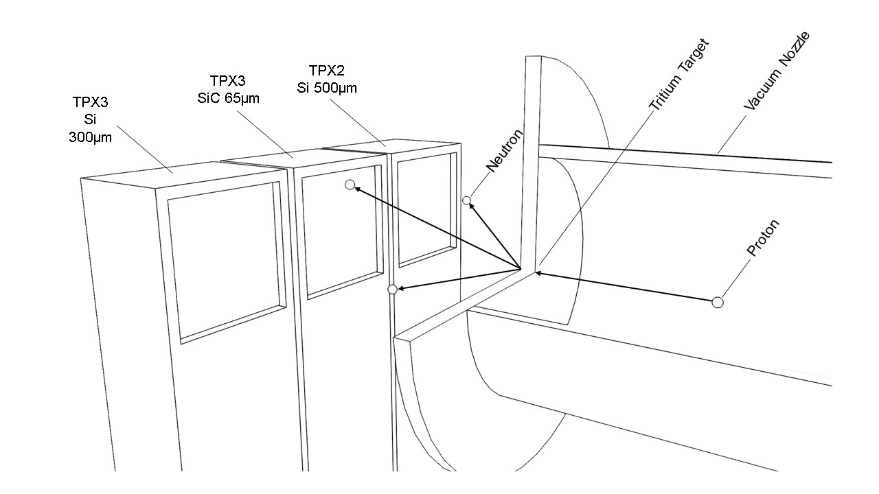
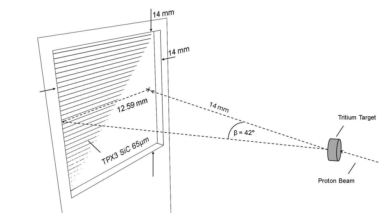
The cluster shape recognition in the SiC pixel sensor allowed for the identification of events corresponding to elastic scattering of neutrons on carbon and silicon nuclei, with a dominant contribution from the silicon scattering resonance at En≈565 keV. The resulting radial scattering patterns corresponding to elastic scattering of neutrons on Si and C were observed at the expected positions as the proton energy changed (Figure 2). The approach and results will be presented demonstrating that the proposed method allows for neutron spectrometry with energies in the range from 200 keV - 1 MeV even in complex n-gamma radiation fields.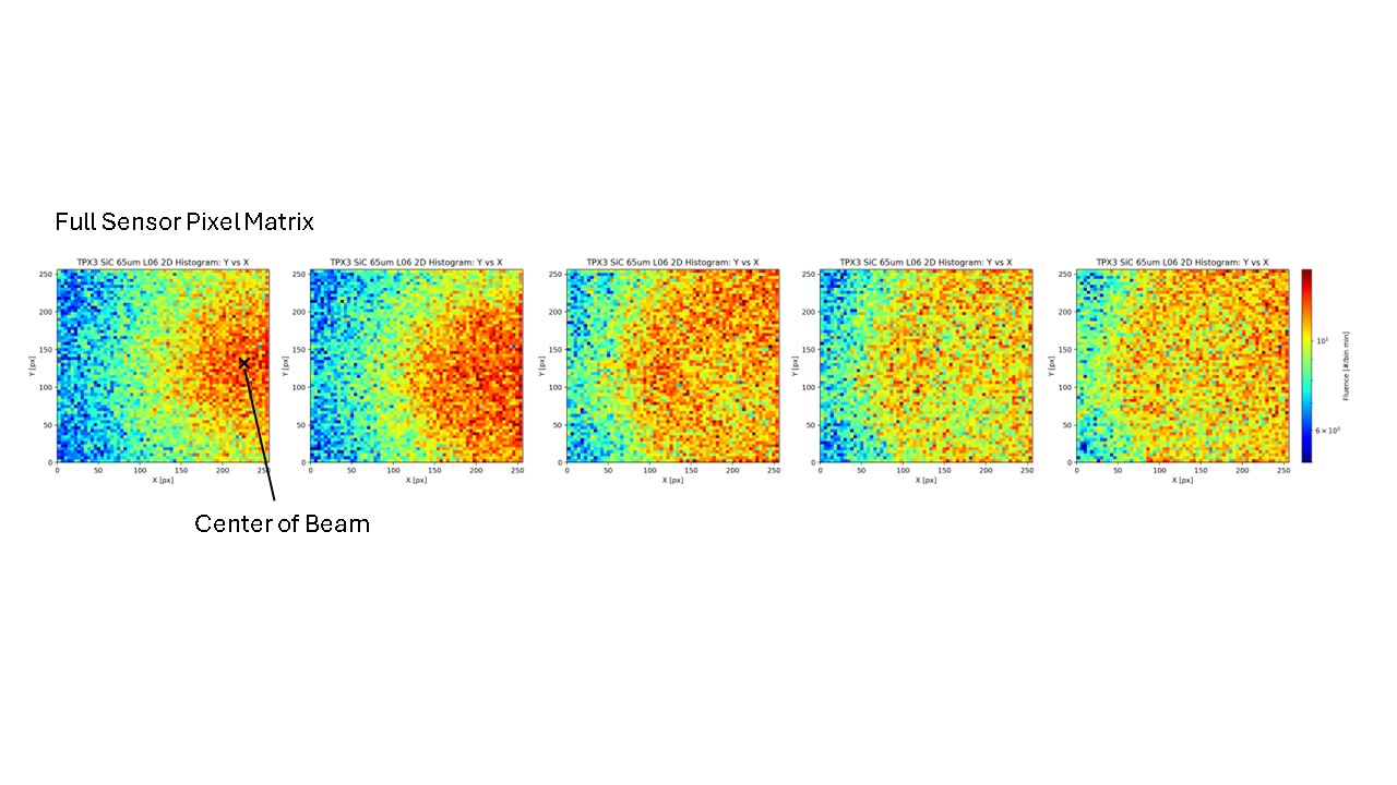
1 B. Zatko et al., From a single silicon carbide detector to pixelated structure for radiation imaging camera, JINST 17 (2022) C12005.
2 C. Granja et al., Detection resolving power of SiC Timepix3 detector to electrons, neutrons, ions and protons, JINST 19 (2024) C11007.
3 H. Liskien and A. Paulsen, Neutron production cross sections and energies for the reactions T(p,n)3He, D(d,n)3He, and T(d,n)4He, Nuclear Data Tables 11, 569-619 (1973)
[4] B. Bergmann et al., Ionizing energy depositions after fast neutron interactions in silicon, IEEE Transactions on Nuclear Science, Journal Name: IEEE Transactions on Nuclear Science Journal Issue: 4 Vol. 63; ISSN 0018-9499
[5] C. A. Bertulani, P. Danielewicz, Introduction to Experimental Nuclear Reactions, CRC Press, 2004
[6] L. Marek et al., Data Processing Engine (DPE): data analysis tool for particle tracking and mixed radiation field characterization with pixel detectors Timepix, JINST 19 (2024) C04026.
Acknowledgements: Work partially supported by funding grants APVV-22-0382 and DS-FR-24-0020 of the Slovak Research and Development Agency and funded by the EU NextGenerationEU program through the Recovery and Resilience Plan for Slovakia under the project No. 09I05-03-V02-00073.
X-ray detection plays a crucial role in medical imaging, industrial inspection, and security. At present, X-ray detectors are typically categorized into two types: direct conversion and indirect conversion methods. Semiconductor-based direct radiation detection, utilizing materials such as CdZnTe, CdTe, GaAs and metal halide perovskites, has rapidly advanced and demonstrated diverse applications, including X-ray imaging. Direct detectors offer a wide linear response range, rapid pulse rise times, and high energy and spatial resolution.
In this work, a hybrid semiconductor pixelated detector (Timepix) has been used to investigate the imaging quality assessment under low-dose X-ray environment. Timepix3 is a single-photon counting type based readout ASIC chip. The hybrid pixel device, developed at CERN, features a 256 × 256 array of square pixels with a 55 µm pitch and comprises a semiconductor sensor layer (2 mm CdTe in this study) bump-bonded to a readout ASIC. An indirect X-ray detector comprising a CMOS flat-panel sensor coupled with a scintillation film was employed for image quality comparison. The CMOS flat-panel detector features a 512 × 1,024 photodiode array with a pixel pitch of 48 µm and an active area of 24.6 × 49.2 mm². Furthermore, the block-matching and 3D filtering (BM3D) denoising algorithm was applied to the Timepix3 images due to its ability to effectively reduce noise while maintaining edge sharpness and fine structural features. Imaging performance was assessed in terms of spatial resolution, X-ray sensitivity, signal-to-noise ratio (SNR) and X-ray transmission imaging experiments with object phantoms were performed under low-dose conditions.
Single photon counting detectors revolutionized data acquisition at synchrotrons when they were introduced in the mid-2000s and quickly became ubiquitous at beamlines. We believe they will continue to play an important role for diffraction-limited light sources, even as the increased flux makes counting more challenging due to pulse pile-up in the analog front end.
Matterhorn is a new readout chip designed at PSI in UMC 110 nm technology. It features a pixel size of 75 × 75 µm², with four counters per pixel and a configurable counter depth between 4 and 16 bits. The chip is optimized for fast counting, targeting 20 Mcps/pixel with 90% efficiency by using the four counters for pile-up tracking. With 4 × 3.125 Gbit/s serializers, the maximum continuous frame rate is 10 kHz at 16-bit depth, scaling up to 40 kHz in 4-bit mode. The chip can also be configured in gating mode for pump probe experiments with a design target of 20 ns for the shortest gate. The readout board is based on an Enclustra SOM with a Xilinx Zynq UltraScale+ FPGA and a 100 Gbit/s fiber connection.
In this paper, we present the first characterization of the full-size 256 × 256 pixel chip bump-bonded to a 320 µm thick silicon sensor, as well as the design of the 500k module, which will serve as a building block for large-area detectors.
We present an implementation of edge AI to compress data on an in-memory analog content-addressable memory (ACAM) device. A variational autoencoder is trained on a simulated sample of energy measurements from incident high-energy electrons on a generic three-layer scintillator-based calorimeter. The encoding part is distilled into tabular format by regressing the latent space variables using decision trees, which is then programmed on a memristor-based ACAM. In real-time, the ACAM compresses 48 continuously valued incoming energies measured by the calorimeter sensors into the latent space, achieving a compression factor of 12x, which is transmitted off-detector for decompression. The talk is based on our preprint (arXiv:2602.15990).
Low-Gain Avalanche Diodes (LGADs) are typically fabricated on p-type substrates, following an n–p$^+$–p junction configuration, where a boron-doped layer forms the gain region.
This architecture is considered optimal for timing and particle-tracking applications since the primary charge carriers initiating the avalanche process are electrons, which feature higher drift velocity and ionization coefficient compared to holes. However, for the detection of low-penetrating particles, such as soft X-rays, the conventional p-on-n configuration becomes less efficient. In these cases, most carriers are generated close to the front junction (n-type region) or within the high-field gain layer, resulting in reduced gain and possibly lower signal-to-noise ratio (SNR).
To overcome these limitations and improve the detection efficiency of low-energy photons and particles, LGADs on n-type substrates (N-LGADs) have been recently proposed. This inverted doping configuration, compared to standard LGADs, is expected to deliver higher gain and SNR for low-penetrating radiation, particularly for X-rays below 1~keV.
The fabricated N-LGADs employ 55 µm-thick n-type epitaxial substrates, with the front junction formed by boron ion implantation. Several junction depths and doping profiles have been implemented to investigate QE and Gain vs interaction depth as a function of junction design. Electrical characterization (I-V, C-V, and gain measurements) will be presented for the different splits, along with optical characterization in the 380–950 nm wavelength range. The latter enables the determination of Gain and QE as a function of the charge generation depth, providing a comprehensive comparison among the various device configurations.
The increasing integration density of silicon pixel sensors, together with emerging applications such as module-level power conversion and enhanced on-detector signal processing, significantly raises the demand for advanced thermal management solutions. Efficient heat removal at the module level is becoming a critical requirement for ensuring stable and reliable operation. In this work, we demonstrate the use of nanowire-based interconnects to improve the thermal coupling between a silicon die and a heat sink, achieving superior performance compared to conventional thermal interface materials such as conductive pastes.
Two bonding approaches for nanowire integration, adhesive bonding and sintering, are presented and systematically compared in terms of thermal efficiency, bonding process requirements, and bonding process demands. The advantages and constraints of each method are discussed, highlighting their suitability for different integration scenarios. Furthermore, we demonstrate that these bonding technologies can be employed not only to enhance thermal conduction but also to mechanically mount silicon pixel sensors onto supporting structures. This dual functionality provides both improved heat dissipation and robust mechanical stability using minimal material.
Together, the presented thermal and mechanical bonding strategies offer a scalable pathway to enhance module-level thermal stability, supporting the performance and longevity of future high-density detector systems and related applications.
Digital tomosynthesis (DTS) is a limited-angle imaging technique that provides volumetric information at a fraction of computed tomography (CT) dose [1]. However, the restricted angular coverage inherently produces out-of-plane artifacts, degrading slice selectivity and contrast-to-noise ratio (CNR). Slice-thickness filtering (STF) applied after filtered back projection (FBP) reconstruction is a well-established approach for suppressing such artifacts [2]. However, conventional STF employs fixed spectral apodization parameters optimized for nominal conditions and therefore cannot adapt to elevated noise in sparse-view or low-dose acquisitions. In this study, we propose a noise-adaptive slice-thickness filtering (NASF) method, in which the fixed spectral apodization term is replaced with a noise-adaptive weighting function derived from the noise power spectrum (NPS) of the reconstructed volume. The NPS is estimated from homogeneous background regions, and the resulting spectral energy distribution is used to automatically control the strength of high-frequency suppression. This allows the filter to adapt its spectral response to the actual noise level, while the slice-thickness component remains unchanged, preserving geometric slice selectivity. Figure 1 illustrates the overall NASF framework. To experimentally validate the proposed method, DTS projections of a chest phantom were acquired over an angular range of ±20° using 50 projections. Figure 2 shows the reconstruction results. Compared with both FBP and conventional STF, NASF effectively suppresses out-of-plane artifacts (red arrows) while preserving structural details. Figure 3 summarizes the quantitative evaluation using the ROIs shown in Figure 2. NASF achieved full width at half maximum (FWHM) of approximately 25.5 mm in the artifact spread function (ASF), comparable to that of FBP (25.2 mm), while improving CNR to 4.1, corresponding to a 23.1% increase over conventional STF (3.4) and a 53.4% increase over FBP (2.7). These results demonstrate that NASF enables noise-adaptive artifact suppression without compromising spatial resolution, offering a practical alternative to fixed-parameter STF for DTS reconstruction.
Photon-counting computed tomography (PCCT) has attracted considerable interest as a next-generation medical X-ray imaging modality because of its high spatial resolution, intrinsic spectral sensitivity, and improved dose efficiency [1]. While current commercial PCCT systems mainly employ direct-conversion semiconductor detectors, indirect photon-counting detectors based on scintillators and silicon photomultipliers are also being investigated as future alternatives [1,2]. In such high-flux X-ray imaging systems, nanosecond-scale scintillation decay times are essential for suppressing pulse pile-up and maintaining high count-rate capability [2]. Therefore, a measurement framework that enables precise and quantitative evaluation of short scintillation decay constants under X-ray excitation is required. In this work, we numerically investigate a frequency-domain approach for evaluating scintillation decay time constants under sinusoidally modulated X-ray excitation.
Frequency-domain lifetime measurements based on modulation depth and phase lag are well established in luminescence spectroscopy [3], and their applicability to scintillator-related materials has been demonstrated for ZnSe-based scintillators [4]. In contrast, radioluminescence decay under X-ray excitation has mainly been studied in the time domain, for example by time-resolved X-ray excited optical luminescence techniques [5].
In this study, the scintillation process was modeled as a linear response system, and the amplitude ratio $|H(\omega)|$ and phase lag $\angle H(\omega)$ of the radioluminescence signal relative to the X-ray modulation were calculated over a modulation-frequency range from 1 kHz to 100 MHz. Representative scintillators, including NaI(Tl), CsI(Tl), Gd$_3$(Al, Ga)$_5$O$_{12}$(Ce) (GAGG), Bi$_{4}$Ge$_3$O$_{12}$ (BGO), CdWO$_4$ (CWO), and CeBr$_3$, were compared. A triple-component decay model was also examined using $\beta$-Ga$_2$O$_3$.
As shown in Fig. 1, the calculated frequency responses clearly depend on the decay time constant. Faster scintillators maintain higher amplitude ratios and smaller phase lags up to higher frequencies, whereas slower scintillators exhibit earlier roll-off and larger phase lags. Distinct separation among representative scintillators was obtained in both amplitude and phase responses, indicating that decay constants can be estimated by combined fitting of these quantities. In the multi-component case, non-monotonic phase behavior was observed, suggesting the possibility of identifying multiple decay channels in the frequency domain.
These results support the feasibility of lock-in-based radioluminescence measurements using a modulated X-ray source and provide a design basis for experimental validation of scintillation lifetime metrology for high-count-rate X-ray imaging applications.
[1] F. R. Schwartz et al., Radiology 314 (2025), e240662.
[2] J. J. van Blaaderen et al., Chem. Mater. 37 (2025), 1716–1740.
[3] N. Boens et al., Anal. Chem. 79 (2007), 2137–2149.
[4] J. Mickevičius et al., Nucl. Instrum. Methods Phys. Res. A 610 (2009), 321–324.
[5] M. J. Ward et al., J. Phys.: Conf. Ser. 425 (2013), 092006.
Compared with the current LHC CMS tracker, the new CMS tracker of the High-Luminosity LHC is undergoing significant enhancements, including the development of a new silicon detector system with improved radiation hardness, higher granularity, and extended coverage up to a pseudorapidity of |η|∼4. In addition, the outer tracker (OT) will be equipped with two types of pT modules (2S and PS) that will provide tracking information to the L1 trigger of the HL-LHC CMS detector, by rejecting signals from particles below a certain pT threshold. Hence, the pT modules must be assembled with a high quality control system and have to pass strict requirements. In this talk, I will present the overview of 2S module production, and representative problems and experience acquired during module assembly and performance test. Some new techniques that have been developed during the module production will also be discussed.
Spectral performance in hyperspectral X-ray imaging using the HEXITEC 6×2 detector system is optimised through systematic parameter tuning and spectral data processing. The approach aims to improve energy-resolved imaging and enhance the quality of spectral information.
Data acquisition and processing are carried out using the Odin software framework, with particular attention to parameters influencing detector response. A structured optimisation strategy is applied to evaluate the impact of key acquisition and processing parameters on spectral quality, including noise characteristics, energy resolution, and count rate performance.
Comparisons between simulated and experimentally acquired spectra are performed to assess the effectiveness of the optimisation. Experimental studies are conducted on representative samples to evaluate material discrimination under different parameter conditions.
The results highlight the sensitivity of spectral performance to detector configuration and identify parameters that significantly influence energy resolution and spectral fidelity. Improved agreement between simulated and experimental spectra is observed following optimisation. These findings support the development of more reliable spectral imaging and contribute to ongoing improvements in colour X-ray imaging methodologies.
[1] K. Taguchi et al., Med. Phys. 40 (2013), 100901
[2] M. C. Veale et al., Synchrotron Radiat. News 31 (2018), 28–32
[3] M. Wilson et al., IEEE Trans. Nucl. Sci. 56 (2009), 2505–2512
[4] L. Jowitt et al., JINST 17 (2022), P01012
[5] S. D. M. Jacques et al., Nanoscale 6 (2014), 11271–11277
[6] C. K. Egan et al., Sci. Rep. 5 (2015), 15979
A new concept of tracking detector based on Scintillating Fibres (SciFi) read out with multichannel silicon photomultipliers (SiPMs) was installed during the upgrade I of the LHCb experiment at CERN. One of the main challenges that the SciFi tracker will face during its operation is the high radiation environment due to fast neutrons. In view of LHCb Upgrade II in 2033, the radiation levels will increase significantly and the SciFi tracker must undergo a major upgrade. By the end of lifetime, the expected radiation fluence reaches 3E12 neq/cm2 at the SiPMs location. To cope with the increase in radiation, cryogenic cooling with liquid nitrogen is being investigated as a possible solution to mitigate the performance degradation of the SiPMs induced by radiation damage.
Under this scenario, different layouts of SiPMs modules from two producers (FBK and Hamamatsu) are being investigated. Several modules were irradiated at Ljubljana at different neutron fluences and have been tested in a dedicated cryogenic setup down to 100 K, where the main key operational parameters were measured as a function of the temperature [1, 2].
In Figure 1 left, the breakdown voltage (Vbd) against temperature is shown for one of the irradiated FBK modules. It is reported a linear decrease of 31,5 mV/K till around 210 K, and below this temperature the linear decrease is not maintained as the Vbd decreases slower with temperature. In Figure 1 right, the dark count rate (DCR) against temperature is shown for the FBK SiPMs at four different irradiation fluences. At the selected overvoltage (8 V), it is reported a decrease of DCR of almost 5 orders of magnitude from RT down to 100 K. Also, above1E12 neq/cm2 it is observed an excess on the measured DCR as is not increasing proportional with the irradiation fluence anymore. The source of this excess DCR it is not clear yet and further studies are needed.
In parallel, a novel concept of integrating microlenses (uLens) at the wafer level, aligned with the SiPM pixel structure, has been developed to enhance photon collection and increase photon detection efficiency (PDE) [3]. The performance of the microlens depends on key geometrical and optical parameters such as uLens curvature, height, diameter, refractive index, pixel pitch, and alignment accuracy. These parameters were optimized through a validated simulation framework that includes realistic optical effects such as refraction, reflection, and angular acceptance, and the main implementation variables are summarized in Figure 2. Accurate fabrication and alignment are essential to achieve the expected performance gains; therefore, the residual layer thickness (RLT) and the alignment of the uLens relative to the SiPM pixel center were measured using mechanical profilometry and microscopy.
An example of these laboratory measurements is shown in Figure 3, demonstrating that the uLens geometry and placement meet the design tolerances and ensuring efficient light focusing with minimal crosstalk. The uLens integration significantly improves PDE by concentrating incoming photons onto the active microcells, effectively increasing the fill factor without changing pixel size. Both simulations and experimental measurements indicate a PDE gain of up to 15–30%, depending on the incident light angle and uLens geometry, and one example of the measured improvement is presented in Figure 4. This enhancement not only increases sensitivity but also benefits timing performance [4], making uLens a promising approach for the SciFi tracker upgrade.
HEPS (High Energy Photon Source) is the first fourth-generation light source in China, featuring high-energy, high-luminosity X-rays. Since more than half of its end stations generate photon energies above 25 keV, high-Z detectors are essential. Additionally, advanced experiments such as X-ray Photon Correlation Spectroscopy (XPCS) and ultrafast dynamics studies necessitate detectors with high frame rates. To meet the demand for a high-speed, high-Z pixel detector at HEPS, a readout ASIC named HouYi has been developed
HouYi is a charge-integration readout chip operating in burst mode, designed for compatibility with electron-collecting sensors like CZT and CdTe. It features a pixel pitch of 150 μm × 150 μm, with an array size of 64 × 64 in the engineering run. The burst frequency is adjustable from 1 MHz to 4.7 MHz. To achieve both single-photon sensitivity and a high dynamic range, the chip incorporates a two-stage adaptive gain front-end circuit. Following charge integration, signals are stored in a 32-cell analog memory array, enabling successive sampling of 32 frames. The corresponding gain settings are also stored in analog form by converting a 2-bit digital gain signal into analog voltage levels. Finally, signals are read out via four differential drivers during the intervals between photon bunches.
HouYiV01S is the first small-scale prototype, containing a 32 × 32-pixel array with full functionality. A die photograph is shown in Figure 1. Performance tests confirm its proper operation. As demonstrated in Figure 2, the chip can integrate, store, and read out 32 pulses at frame rates up to 4.7 MHz. At a photon energy of 30 keV, the signal-to-noise ratio of the preamp exceeds 10, indicating the capability for single-photon resolution. Figure 3 presents the transfer characteristics of the dynamic range, which extends to approximately 4300 photons at 30 keV. The overall nonlinearity of the signal chain is below 4 %.
The China Spallation Neutron Source (CSNS) is currently upgrading to CSNS-II, increasing the proton beam power to 500 kW and constructing several new neutron spectrometers. The CSNS-II upgrade poses significant challenges for detector and electronics systems, including higher counting rate, improved position resolution requirement, and vacuum operating environment. In this paper, we present an ultra-low-power front-end readout electronics prototype designed for ³He tube detectors in CSNS-II spectrometers. The circuit design, FPGA algorithms, and laboratory test results of the prototype will be discussed. Experimental results demonstrate that the new electronics system can achieve a single-tube counting rate of 100K/s while maintaining a position resolution better than 8 mm. Test also confirmed the system's capability to operate under vacuum conditions. These results meet the requirements for neutron signal readout in CSNS-II spectrometers.
Diamond detectors have been studied since long, its radiation hardness makes it appealing for beam monitoring application and its tissue equivalence makes it attractive for radiotherapy or dosimetry. Its low leakage current allows to operate diamond detectors without doping.
Single crystal diamond is vastly used, but to approach a most cost effective material, here a polycrystalline diamond is studied. The polycrystalline diamond presents trap centres in the grain boundaries that diminish the charge collection distance. Besides, polarization effects emerge during time changing the electric field and showing a decrease in the charge collection distance. Pumping the diamond, exposing it to radioactive sources without bias voltage, create electron holes pairs inside the diamond that then fill some trap centres and increase the charge collection distance.
For this presentation, results of the pumping and unpumping mechanisms for a polycrystalline diamond detector are presented. In depth studies will be shown for the trapping centres inside the diamond.
Over the last two decades, Hybrid Photon-Counting (HPC) pixel detectors have revolutionised and enabled a wide range of techniques at synchrotron light sources. These achievements are driven by their high frame rates, large dynamic range, radiation hardness, high DQE, and no noise associated with the readout operation [1]. However, the impact of HPC detectors has so far been largely confined to the tender and hard X-ray regimes, while the soft X-ray range remains comparatively inaccessible. DECTRIS lowest energy detectors are those from the PILATUS series, which achieve energy thresholds as low as 1.6 keV [2,3].
DECTRIS is actively pushing the lower energy boundary. This contribution presents ongoing R&D efforts at DECTRIS to extend X-ray photon-counting capabilities towards 1 keV for small-pixel sizes of 75 µm2. Several complementary approaches are being pursued, including optimization of existing detector designs, exploration of novel sensor concepts with internal gain such as Low-Gain Avalanche Diodes (LGADs)—building on the work reported in [4,5]—and the development of a new low-noise application-specific integrated circuit (ASIC).
Characterization results from multiple prototype systems will be presented, based on both in-house and synchrotron beamtime measurements. In addition, the first performance results in ptychography applications at SoftiMAX (MAX IV) and experiments at SIRIUS (SOLEIL) will be shown.
References:
[1] Förster, A., Brandstetter, S. & Schulze-Briese, C. Transforming X-ray detection with hybrid photon counting detectors. Philos. Trans. R. Soc. A 377, 20180241 (2019).
[2] Wernecke, Jan, et al. "Characterization of an in-vacuum PILATUS 1M detector." Synchrotron Radiation 21.3 (2014): 529-536.
[3] O. Chellai et al.; Calibration of a versatile multi-energy soft X-ray diagnostic for WEST long pulse plasmas. Rev. Sci. Instrum. 1 April 2021; 92 (4): 043509. https://doi.org/10.1063/5.0043456
[4] Zhang, J., et al. “Development of LGAD sensors with a thin entrance window for soft X-ray detection.” Journal of Instrumentation 17.11 (2022): C11011.
[5] Baruffaldi, F., Bergamaschi, A., Boscardin, M. et al. Single-photon counting pixel detector for soft X-rays. Commun Phys 8, 321 (2025). https://doi.org/10.1038/s42005-025-02240-9
We acknowledge MAX IV and SoftiMAX, in particular K.Thanell, I. Beinik, and J.Schwenke, for close collaboration, enabling calibration, characterization, and application results. We also acknowledge SOLEIL SIRIUS, especially M. Chauvin, A. Dawiec, M. Andrä, K. Paton, P. Fontaine, and G. Ciatto, for beamline access, characterization, and XRD measurements.
Speckle-based X-ray dark-field imaging is attractive because it can deliver small-angle scattering contrast with a comparatively simple optical setup, but quantitative modeling of weakly absorbing microstructures in hydrated environments still requires improved treatment of multiple refraction and unresolved ultra-small-angle X-ray scattering (USAXS). Building on the wave-optics simulation framework of Meyer et al. [1] and motivated by USAXS formulations used in speckle/beam-tracking studies, we developed a plane-wave monochromatic multi-slice simulation pipeline that extends the projection-approximation model with slice-by-slice propagation through the sample, explicit particle-in-water embedding, and detector-plane USAXS blur described by a hybrid model combining an isotropic bulk term with a weak phase-gradient-dependent anisotropic term. Simulations were performed at 17.5 keV with a five-layer random diffuser, a 50 um pixel detector, and a 130 um-thick water cell containing a sparse monolayer of eight 120 um polystyrene-like spheres.
The water-blank normalization effectively removed most box- and water-related attenuation while preserving particle-specific dark-field contrast. Residual normalized transmission deviations were only on the order of 10-4 and the absorption CNR was 1.72, whereas the dark-field extinction remained strong and spatially localized to the particle footprints, with -ln(D) = 0.2349 in particle regions versus 0.0052 in the surrounding local background. The resulting dark-field CNR reached 29.18, corresponding to an approximately 17-fold contrast advantage over absorption. The retrieved mean speckle size was 161.7 um (about 3.23 detector pixels), and the equivalent detector-plane USAXS blur was 0.67 detector pixels. These results show that explicit multi-slice propagation and USAXS-aware modeling can recover robust dark-field signatures from weakly absorbing particles embedded in water, where conventional attenuation contrast is strongly suppressed.
Resistive Plate Chambers (RPCs) are gaseous detectors widely used in particle physics, for example, in the muon system of the CMS detector at the CERN Large Hadron Collider (LHC), as they provide fast timing information for efficient muon triggering. In view of the upcoming High-Luminosity (HL) LHC phase, an improved RPC detector (iRPC) has been developed to cope with the significantly higher particle rates and radiation levels expected during future operation.
The upgraded detectors are designed to extend the geometrical acceptance of the CMS muon trigger system toward the high pseudorapidity region, up to |η| ≈ 2.4. From a technological perspective, iRPCs feature a reduced gas gap and thinner electrodes compared to conventional RPCs, together with low-resistivity electrode materials. These design choices allow efficient operation in high-rate environments while maintaining good timing performance and detector stability.
In addition, the reduced charge delivered per avalanche results in smaller signals, requiring the use of dedicated and highly sensitive front-end electronics and is expected to mitigate aging effects under the demanding HL-LHC conditions.
Performance studies of the iRPC prototype have been carried out at the Gamma Irradiation Facility (GIF++) at CERN, demonstrating stable operation and high efficiency under intense background conditions with irradiation rates up to about 2 kHz/cm².
In parallel, dedicated R&D activities are ongoing to identify environmentally friendly gas mixtures for RPC operation, motivated by the need to replace high Global Warming Potential gases currently used in the CMS RPC system.
This contribution presents recent results on the performance and validation of the iRPC prototype under high background conditions, as well as ongoing investigations of eco-friendly gas mixtures for future RPC operation.
This work investigates the impact of irradiation on the timing performance of 3D silicon devices and electric field and charge collection uniformity. The study is organized in two parts. First, the response of irradiated and non-irradiated double-sided 3D CNM devices is compared. Second, the performance of a 3D IMECAS device is analyzed when un-irradiated and irradiated; this device incorporates a 2 μm wide square trench electrode and a central electrode with a diameter of 0.5 μm.
The results highlight two main effects. First, irradiation reduces the influence of geometrically induced low-field regions, thereby suppressing the slow component of charge collection and significantly shortening the long tails observed in the signal waveforms. This leads to an improvement in timing response. Second, although irradiation decreases the signal amplitude, this loss can be compensated by the higher electric field developed in the device, which enhances charge multiplication in 3D IMECAS devices with gain. This effect is an intrinsic feature of 3D geometries with very small electrode radii, where strong local electric fields can be established. Despite the high electric field near the electrode tip, in the 3D Imecas device, the device remains stable due to a self-quenching mechanism that limits the multiplication process. These results indicate that, irradiation can mitigate detrimental waveform components while preserving stable operation and improving timing performance.
Gaseous detectors play a crucial role in high energy physics experiments, yet their operation often relies on fluorinated gases with a very high Global Warming Potential (GWP). Resistive Plate Chambers (RPCs) operated in avalanche mode typically use high performance gas mixtures based on high-GWP F-gases such as C₂H₂F₄ and SF₆.
As environmental concerns grow and regulations become increasingly stringent, the development of sustainable gas mixtures has become a global priority.
Within the RPC ECOGas@GIF++ Collaboration, a long term R&D program has investigated eco-friendly gas mixtures for RPCs and assessed their performance under irradiation. RPCs operated with an HFO-1234ze/CO₂ mixture were exposed to high particle fluxes at CERN GIF++, accumulating O(10² mC/cm²) over three years. This ageing campaign is now complete, and the detectors’ performance has been systematically evaluated across a broad range of rates.
This talk will present preliminary final results from the campaign, along with future perspectives.
Photon scatter remains a major source of image degradation in Single Photon Emission Computed Tomography (SPECT), leading to reduced contrast recovery and quantitative accuracy. Conventional reconstruction frameworks typically reject these scattered events. This study investigates the utility of rejected scattered data as a "scatter-informed" initial estimate for Maximum Likelihood Expectation Maximization (MLEM) [1] reconstruction to improve convergence and image quality in low-count conditions. Simulations were performed using the SIMIND [2] Monte Carlo toolkit, modelling a high-resolution SPECT system with a Jaszczak phantom containing six hot spheres (radii: 0.80 - 3.00 cm) and a 4:1 activity concentration ratio of $^{99m}Tc$ radionuclide. The primary photopeak energy of $^{99m}Tc$ is 140 keV. Scatter was estimated using the Triple Energy Window (TEW) method, with the primary photopeak at 130–150 keV and adjacent scatter windows at 120–130 keV and 150–160 keV.
We compared attenuation corrected reconstructed images from a uniform initial estimate and scatter-derived initial estimate generated by back-projecting the TEW scatter profiles for 25 MLEM iterations using CASTOR [3] software. The Fig. 1 shows central trans-axial slices of the Jaszczak phantom reconstructed at different MLEM iterations for the two initialization strategies. Results demonstrate that the scatter-derived initialization yields notable improvements at early iterations; as illustrated in Fig. 1 ($4^{th}$ iteration), it achieves visibly reduced background noise while preserving contrast compared to the uniform initialization.
Fig.1 The top row shows images reconstructed using uniform initial estimate, and the bottom row shows images reconstructed using TEW-based scatter estimate. The images are normalized.
Quantitative evaluation was performed using NEMA-based metrics [4], including Contrast Recovery Coefficient (CRC), Coefficient of Variation (CoV), and Contrast-to-Noise Ratio (CNR) as defined below:
$$ CRC=\frac{\left(\frac{C_{hot}}{C_{bkg}}-1\right)}{A-1}, COV=\frac{\sigma_{bkg}}{C_{bkg}}\ , CNR=\frac{C_{hot}-C_{bkg}}{\sigma_{bkg}}\ . $$ where, $C_{hot}$ is measured average counts in the region of interest (ROI), $C_{bkg}$ is corresponding average background counts, $\textbf{A}$ is the true hot to background Ratio and, $\sigma_{bkg}$ is standard deviation of the background ROI counts. At the $4^{th}$ iteration, CRC improves by approximately 12-18\% across sphere sizes, while CNR shows an enhancement of 15-20\% compared to uniform initialization at comparable noise levels. Fig. 2 shows that the scatter-informed approach achieved a peak CNR at the $4^{th}$ iteration for largest sphere. In contrast, the uniform estimate required 14 iterations to reach its peak CNR. These improvements are accompanied by better visual delineation of structures and reduced background contamination. Fig.2 CNR as a function of MLEM iteration number for reconstruction using uniform and scatter initial estimates. Maximum CNR for biggest sphere are marked with arrows. However, at higher iterations, the benefit diminishes due to noise amplification inherent in the scatter derived image. This is evident in Fig. 1 ($12^{th}$ iteration), where pronounced boundary artifacts begin to emerge. This study highlights that scattered photons, typically discarded, contain valuable spatial information that can be leveraged to enhance early-iteration image quality. The proposed scatter-informed initialization provides a practical pathway for improving reconstruction performance in low-count and high-scatter imaging scenarios, with potential implications for accelerated and dose-efficient SPECT imaging.
[1] Lawrence A Shepp and Yehuda Vardi. Maximum likelihood reconstruction for emission tomography. IEEE transactions on medical imaging, 1(2):113–122, 2007.
[2] Michael Ljungberg et al. The simind monte carlo program. Monte Carlo calculation in nuclear medicine: Applications in diagnostic imaging, pages 145–163, 1998.
[3] Thibaut Merlin et al. Castor: a generic data organization and processing code framework for multi-modal and multi-dimensional tomographic reconstruction. Physics in Medicine & Biology, 63(18):185005, 2018.
[4] NEMA et al. Nema standards publication nu 1-2018: Performance measurements of gamma cameras. Rosslyn Virginia: National Electrical Manufacturers Association, 2018.
Anger Cameras have been widely used in nuclear medicine, presenting, however, limitations in detection efficiency for higher photon energies and sensitivity due to the presence of a lead collimator. Compton Cameras (CC) are potential competitors, primarily because they improve sensitivity in imaging radioactive sources by eliminating the mechanical collimator. In a CC, physical collimation is not used, conferring the potential to improve the quality of nuclear medicine images and reduce patients’ radiation exposure. The detection of scattered photons and recoil electrons, as well as energy determination allows the construction of a conic surface indicating the possible region of the photon’s primary interaction. The intersection of all conic surfaces shows the most probable location of the source.
A CC based on a Gaseous Detector is being developed within the DRIM group [1], with the potential to enhance the sensitivity compared to other CC concepts, since it detects scattered photons across a 4π solid angle using only one detector. In this scope, a simulation study was conducted with a radioactive point source to evaluate the feasibility of the proposed solution, whose results will be presented, namely, photon and electron interactions, energy spectra, and reconstructed images.
Silicon carbide provides significant advantages as a radiation sensor, such as high radiation hardness and wide temperature operation, suitable for application in nuclear energy, accelerator physics research, particle therapy and outer space. Combined with the high spatial segmentation of pixel imagers and noiseless counting response of Timepix chip [1], high-resolution radiation measurement techniques [2] can be exploited also with SiC sensors [3,4]. We apply the spectral-tracking imaging ability of single particles to examine and evaluate the sensitivity and tracking resolving power of SiC to fast neutrons. The active thickness of the sensor, regulated by varying the applied bias [5], determines the particle track morphology and their charge collection as well as the detection efficiency of the fast neutrons.
In this work we experimentally examine the imaging-tracking response of Timepix3 detectors equipped with 4H-SiC sensors to 14 MeV neutrons at various active sensor thicknesses controlled by applied bias. The sensor was prepared from 80 µm thick epitaxial 4H-SiC layer grown on 350 µm thick base 4H-SiC substrate. The sensor bump-bonded to Timepix3 chip is readout as 256 × 256 (65536) pixels of Schottky electrodes with 55 µm pitch. The reverse biasing from 50 to 200 V modifies the active sensor thickness from 38 to 76 µm [5]. The neutrons were generated by DT neutron generator at DANAIDES facility at CEA in Cadarache.
The measured data consisted of a mixed radiation field comprising photons, electrons, protons, ions and alpha particles produced by neutron interactions in the sensor material and surrounding structures including secondary radiation background. The detector raw data were pre-processed at the pixel-chip level with the TraX Engine SW tool [6]. Further post-processing at the detector and radiation environment level were done with customized scripting where single-track morphology and spectral cluster parameters such as deposited energy and track length were further analyzed. Particle discrimination is based on prior experimental calibrations on well-defined radiation fields. Double-parameter functional filters were applied to separate events according to their energy deposition characteristics and spatial properties. Based on these criteria, the events were classified into two groups: high energy transferring particles (HETP), representing the products of neutron interactions with Si and C nuclei, and low energy transferring particles (LETP) representing the background accompanying the neutron source.
The sensor bias significantly affects the response of the SiC Timepix3 detector to 14 MeV neutrons. The experimental results show increase in the number of detected neutron-induced events with increasing bias, consistent with the enlargement of the depleted region. Moreover, the applied bias influences the morphology of clusters produced by highly ionizing recoil particles originating from neutron interactions in the sensor material. (fig. 1 a - e) With increasing bias, an increase in cluster size is observed. This effect is attributed to the stronger and deeper electric field within the sensor, which enhances lateral carrier transport and charge sharing between neighboring pixels. At higher bias voltages, a saturation effect is observed. This effect manifests as a redistribution of charge within large clusters, where the central pixel exhibits reduced collected charge compared to surrounding pixels. The observed bias dependence of cluster size, charge sharing, and volcano effect demonstrates the strong influence of the electric field configuration on the detector response to neutron-induced heavy recoils. (fig. 2)
[1] E. Heijne, et al., Nucl. Instrum. Meth. A 699 (2013) 198-204
[2] C. Granja et al., Nuclear Instr. Methods A 908 (2018) 60-71
[3] B. Zat'ko et al., JINST 17 (2022) C12005
[4] A. Novak et al, J. of Instrum JINST 18 (2023) C01022
[5] A. Sagatova et al., AIP Conf. Proc. 3054 (2024) 050011
[6] L. Marek et al., JINST 19 (2024) C0
Acknowledgement: This work was partially supported by grants APVV-22-0382 and DS-FR-24-0020 of the Slovak Research and Development Agency and funded by the EU NextGenerationEU through the Recovery and Resilience Plan for Slovakia under the project No. 09I05-03-V02-00073. Carlos Granja was affiliated at Advacam, Prague when the experimental measurements were performed.
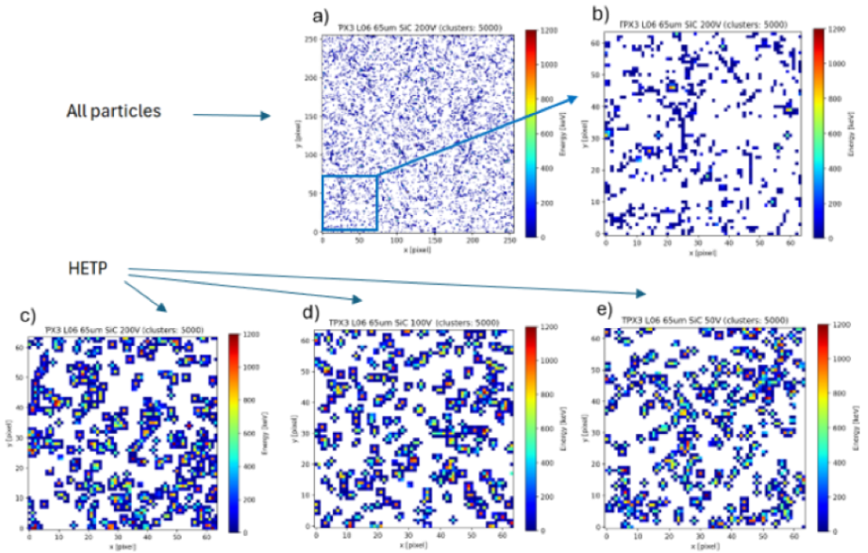
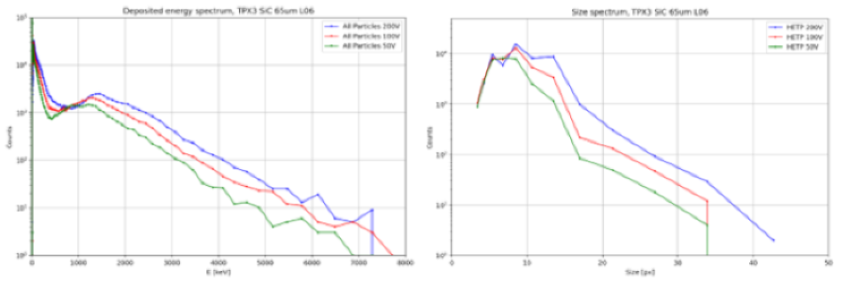
Chanwoo Doo1, Jibum Kim1, Jiho Lee1, Jungwon Kang1, 2, *
1. Department of Foundry Engineering, Dankook University, Yongin-Si, 16890, Gyeonggi-Do, Republic of Korea
2. Department of Semiconductor Convergence Engineering, Dankook University, Yongin-Si, 16890, Gyeonggi-Do, Republic of Korea
* Corresponding author: jkang@dankook.ac.kr
Perovskite-based radiation detectors are attracting attention as next-generation radiation detectors due to their high charge mobility and tunable bandgap (Fig. 1a). However, limited charge collection at the transport layer interface is reported to be a major cause of degraded detection performance. In this study, changes in detection sensitivity were observed by sequentially doping the electron transport layer (ETL: PCBM) and the hole transport layer (HTL: PEDOT:PSS) with molybdenum disulfide (MoS2). In Fig. 1b, the external quantum efficiency (EQE) graph of perovskite MAPbI3 shows that it matches well with the emission spectrum of the CsI(Tl) scintillator used in the indirect detector. Molybdenum disulfide (MoS2) used for charge transport layer doping was selected because it possesses tunable bandgap characteristics and can enhance charge mobility and reduce interfacial defects. Prior to device fabrication, 2D MoS2 nanocrystals were fabricated by centrifugation following liquid exfoliation. Size analysis according to changes in centrifugation speed showed that the average particle size decreased as the centrifugation speed increased from 4,000 rpm to 8,000 rpm, and uniform nanocrystals with an average size of approximately 28 nm were obtained under the 8,000 rpm condition (Fig. 1c).
When the amount of MoS2 added to the HTL was fixed at 1 wt% and the detection sensitivity according to the size of MoS2 was measured, the highest sensitivity of 2.499 mA/Gy·cm² was observed when 28 nm MoS2 was added (Fig. 2a) under X-ray irradiation conditions of 80 kVp, 63 mAs, and 1.57 sec. Experiments were conducted to add MoS2 to the ETL layer using the same method, and the highest sensitivity was observed when 28 nm MoS2 was added. To determine the optimal concentration of MoS2 nanocrystals, the amount of MoS2 added to each transport layer was varied from 1 wt% to 4 wt% (Fig. 2b). When 3 wt% of MoS2 was added to both the ETL and HTL simultaneously, a maximum sensitivity of 2.774 mA/Gy·cm² was obtained (Fig. 3a). This represents a 24.84% improvement compared to the detector without added MoS2, which showed a sensitivity of 2.222 mA/Gy·cm². The defect density and charge mobility were evaluated using the space charge limiting current method (SCLC) (Fig. 3b). As shown in Fig. 3c, the detector with MoS2 added to both HTL and ETL exhibited the lowest defect density of 9.46 × 10¹⁵ cm⁻³ and the highest mobility of 2.23 × 10⁻³ cm² V⁻¹ s⁻¹, indicating improved charge transport and reduced recombination loss compared to the detector without added MoS2.
PCBM : Phenyl-C61-butyric acid methyl ester
PEDOT:PSS : Poly(3,4-ethylenedioxythiophene):Poly(styrenesulfonate)
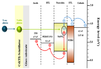
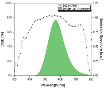
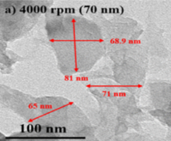
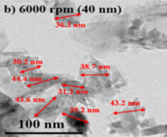
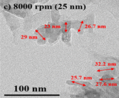
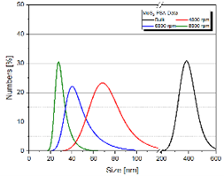
Figure 1. (a) Energy band diagram and carrier transport mechanism of the indirect MAPbI3 X-ray detector. (b) External quantum efficiency (EQE) of the MAPbI3 X-ray detector and the emission spectrum of the CsI(Tl) scintillator (c) TEM images and size distribution of 2D MoS2 nanocrystals obtained at centrifugation speeds of 4000, 6000, and 8000 rpm
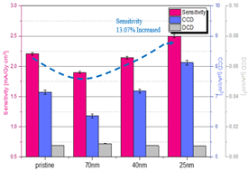
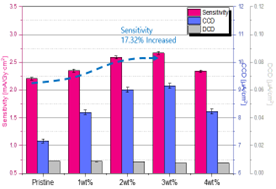
Figure 2. (a) Radiation parameters with different size of MoS2 in the HTL (b) Radiation parameters with different amount of MoS2 in the HTL
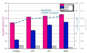
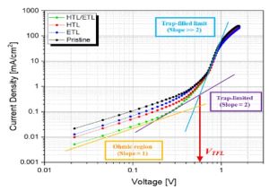
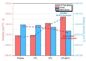
Figure 3. (a) Radiation parameters when MoS2 is added to each transport layer and simultaneously (b) Space charge-limiting current method (SCLC) (c) Defect density and mobility when MoS2 added to each transport layer and simultaneously
The authors acknowledge funding from the Korea Institute for Advancement of Technology(KIAT) grant funded by the Korea Government(MOTIE) (RS-2025-02214408, HRD Program for Industrial Innovation) and National R&D Program through the National Research Foundation of Korea(NRF) funded by Ministry of Science and ICT (RS-2021NR057239)
Timepix3 hybrid pixel detectors [1] are widely used in applications requiring precise radiation spectrometry, including space instrumentation [2], high-energy and nuclear physics [3] or neutron detection [4, 5], where detectors are frequently exposed to varying thermal conditions. Temperature fluctuations can influence the spectrometric response, affecting both the accuracy of energy measurements and the energy resolution.
The temperature dependence of Timepix3 detectors equipped with the Katherine readout system and various semiconductor sensors (Si, GaAs, CdTe, and 4H-SiC) has been previously investigated over a temperature range from −20 °C to 80 °C and for photon energies between approximately 8 and 60 keV. It was shown that while the energy resolution remains relatively stable across the investigated conditions (with Δσ within 1 keV), a systematic temperature-dependent shift of the photopeak position occurs. This effect, which directly impacts the accuracy of energy determination, becomes more pronounced at elevated temperatures, particularly above 60 °C, reaching deviations of up to −17% (observed for the 4H SiC sensor at 80 °C) [6].
To mitigate this effect, a temperature compensation method was developed for each sensor material based on a unified mathematical framework. The approach relies on establishing a linear relationship between the measured and true photon energies at each temperature, followed by modeling the temperature dependence of the linear regression parameters using second-order polynomial functions. By combining these relationships, a temperature-dependent correction function is obtained, enabling compensation of the observed spectral shifts.
The proposed compensation methods allow accurate reconstruction of photon energies across the investigated temperature range without the need for repeated recalibration at each operating temperature, using a well-defined mathematical correction procedure.
[1] T. Poikela, et al., JINST 9 (2014), C05013
[2] C. Granja, et al., JINST 17 (2022) C03019
[3] B. Bergmann, et al. Nucl. Instrum. Methods Phys. Res. A, 978 (2020), 164401
[4] C. Granja, et al., JINST 18 (2023) P01003
[5] P. Rubovič, et al., Nucl. Instrum. Methods Phys. Res. A, 985 (2021), 164680
[6] N. Kurucova, et al. . Presentation #1665, In 2025 IEEE NSS MIC RTSD, Yokohama, Japan, 1 -8 November, 2025. RTSD-08-05. Abstract at p. 1524.
The authors acknowledge funding from the Slovak Research and Development Agency (Research Projects APVV-22-0382 and DS-FR-24-0020) and from the EU NextGenerationEU through the Recovery and Resilience Plan for Slovakia under the project No. 09I05-03-V02-00073.
The ATLAS experiment inner detector will undergo a complete replacement with the all-silicon Inner Tracker (ITk) during the 2027–2029 shutdown, in preparation for operation at the High-Luminosity Large Hadron Collider. The ITk pixel detector, forming the innermost tracking system, is designed to operate under unprecedented radiation levels and particle densities. Its innermost layer (Layer 0) will employ radiation-hard 3D silicon sensor technology capable of withstanding fluences up to 1.7×10^16 " " "n" _"eq" /〖"cm" 〗^2, while the outer layers (L1–L4) will utilize thin n-in-p planar hybrid modules with sensor thicknesses of 100 µm (L1) and 150 µm (L2–L4).
Test-beam campaigns play a crucial role in evaluating sensor and module performance before and after irradiation to HL-LHC levels. In recent years, a broad range of sensor designs from multiple vendors has become available for systematic studies. The 2025 test-beam campaigns introduced new module configurations, including triplet and quad assemblies equipped with the final ITkPixV2 readout chip. Triplet modules integrating 3D sensors with pixel geometries of 50×50" " μ"m" ^2and 25×100" " μ"m" ^2were tested under beam conditions, both before and after irradiation.
Measurements were performed over a range of incident angles to probe charge-collection efficiency under realistic detector operating conditions. The 2025 dataset therefore provides significant new insights into sensor performance, particularly in irradiated scenarios, and contributes to the ongoing qualification of ITk pixel technologies. A subset of these data is currently under detailed analysis.
This contribution presents an overview of the ITk pixel sensor and module qualification program based on test-beam studies, highlighting the latest results from the 2025 and 2026 campaigns.
The High Luminosity upgrade of the Large Hadron Collider at CERN (HL-LHC) will provide unprecedented instantaneous and integrated luminosities of around 5 x 10$^{34}$ cm$^{-2}$ s$^{-1}$ and 3000/fb, respectively. The expected average of 140 to 200 collisions per bunch-crossing (pileup) represents a severe challenge for the detectors. The endcap part of the CMS calorimeters will be replaced by a new detector. In the ECAL barrel, crystals and photo detectors are expected to sustain the new conditions, while the electronics will be completely replaced. The ECAL Very Front End electronics will be equipped with two already produced custom ASICs per crystal: a dual gain trans-impedance amplifier and an ASIC providing two 160 MHz ADC channels, gain selection, and data compression. The noise increase in the photo detectors, due to radiation-induced dark current, will be mitigated by reducing the ECAL operating temperature from 18 °C to 9 °C. The trigger primitive formation will be moved off-detector and performed by powerful and flexible FPGA processors. The upgrade of the ECAL electronics will allow maintaining the excellent energy resolution of the detector and, in addition, greatly improves the time resolution of electrons and photons above 30 GeV, down to a few tens of picoseconds. This presentation will review the final design of the full ECAL barrel readout chain and the status of the individual components R&D. Results from several test beam campaigns at the CERN SPS, using electron beams with energies of up to 250 GeV, will be summarised. In particular, we will present measurements of the energy and timing resolution performance of the latest HL-LHC ECAL readout electronics prototypes.
The MAX IV Synchrotron facility in Lund, Sweden, employs more than 30 X-ray detectors and cameras for the operation of its beamlines.
The most common drivers for the choice of a certain technology are the spatial and temporal resolution, and the energy range. Different detector typologies (imaging, energy sensitive...) and technologies (photon counting, charge integrating...) respond to different experimental requirements.
The facility purchases most of the detectors from commercial partners, but some of the most cutting edge solutions are obtained instead through scientific partnerships with other laboratories. In both cases we take care of the characterization and calibration of all detectors as well as the integration with the rest of the beamline and the IT infrastructure of the laboratory.
We will present an overview of the technologies employed, of the operational aspects and support systems for these detectors.
Two pad sensors of high-flux CdZnTe grown by Redlen Technologies with different anode metallization (platinum and titanium-gold) were characterized under direct X-ray beam in P07 beamline at Petra III, during 40-bunch mode operation. A Transient Current Technique (TCT) readout setup from the University of Hamburg [1] was used, with a homemade Bias-T, a Femto 40 dB 2GHz amplifier and a Tektronix MSO 4104 5GS/s oscilloscope. The transient signal was collected per bunch, using the revolution bunch clock from the storage ring as a trigger. It was possible to observe the transient current signals for each bunch, as illustrated in Figure 1.
The 87 keV beam was defined by slits to 100x100 µm, and the area of the pad sensors was scanned with 200 µm steps for four different attenuations of the beam, with estimated fluxes of 3e+08 photons/second to 1e+09 photons/second. The results show that the full charge was collected by the sensors before 50 ns in most positions. The sensors’ areas show a homogeneous charge collection efficiency. In regions associated with defect vicinities, a longer charge collection time up to 180 ns was observed, indicating delayed charge transport; some regions indicated also an excess of charge (as shown in Figure 2), which can be associated with Excess Leakage Current effects [2]. The different observed pulse shapes further indicate differences in the internal electric field of the sensors, provoked by the different anode electrodes.
[1] J. Becker, PhD thesis, Universität Hamburg (2010).
[2] B.D. Cline et al., JINST 20 (2025), P10021
The High-Luminosity LHC upgrade will require detector systems capable of operating in unprecedented particle rates and radiation environments. To meet these challenges and maintain efficient muon triggering and reconstruction, new Gas Electron Multiplier (GEM) ME0 detectors will be installed in the forward region of the CMS experiment, complementing the already installed GE1/1 GEM detectors and extending the pseudorapidity coverage of the muon system to |η| < 2.8.
This talk will present the role of the broader GEM detector program in CMS, highlighting how improved redundancy, enhanced muon identification and better background rejection will significantly extend the physics reach of the CMS muon system. The performance of the installed GE1/1 station during Run 3 will be reviewed. In addition, the first results for the ME0 stations, including their detector design and operational performance, will be discussed.
A 2 x 6 HEXITEC (High Energy X-ray Imaging Technology) detector has been developed through a collaboration between STFC (Science and Technology Facilities Council) and NXCT (The UK’s National Research Facility in X-ray Computed Tomography). HEXITEC is a direct-conversion CdTe-based hyperspectral X-ray detector that features an 80 x 80 pixel array with a 250 µm pixel pitch [1]. The 2 x 6 HEXITEC comprises 12 single-module HEXITEC detectors mounted together in a tiled architecture [2] to expand the effective field-of-view (FOV) to approximately 12cm x 4cm, allowing for larger-area acquisitions while retaining hyperspectral capability (<1 keV energy resolution). While this increased coverage supports a wider range of samples, it also introduces additional challenges related to data transfer throughput, detector uniformity and system stability.
To explore these capabilities, NXCT is establishing a colour imaging user system (figure 1) at the University of Manchester in collaboration with the University of Ghent. The colour imaging system aims to integrate the large FOV and hyperspectral X-ray capabilities of the 2 x 6 HEXITEC within an existing micro-CT unit (NIKON 225KV reflection source), providing users with access to hyperspectral X-ray CT (HXCT) for a variety of samples up to ~10cm in size. The foreseen applications span a wide range of fields including materials science, cultural heritage, and industrial inspection [3].
The colour imaging system is currently in the commissioning phase, with ongoing work focused on detector integration into the existing micro-CT system, detector calibration and validation, system stability, and acquisition workflow development. Important technical progress has already been made in addressing the increased data collection and transfer requirements. This includes a node-based acquisition system capable of managing the large hyperspectral data rates (~11 Gb/s), generated in parallel by the 12 individual HEXITEC modules.
These data transfer advances have allowed for the acquisition of the first projection image using the 2 x 6 HEXITEC system (figure 2). An in-house, multi-material sample consisting of zirconium and silver pieces, as well as varying concentrations of copper and tin mixtures, has been used as an initial test sample. Preliminary analyses of these projection images have been performed using an in-house ROI-based occupancy and spectral measurement tool, providing an initial framework for optimising acquisition parameters and developing data processing approaches.
Developed within the Medipix4 Collaboration, the Timepix4 ASIC is a versatile hybrid pixel detector featuring a 448×512 pixel matrix with 55 µm pitch and supporting both data-driven and frame-based readout [1], making it suitable for photon-counting and spectrally resolved imaging. This contribution describes the implementation and performance evaluation of Timepix4 assemblies equipped with GaAs and CdTe sensors at the INFN-PEPI facility in Trieste [2]. This laboratory is equipped with a compact micro Computed Tomography (μCT) system that allows the use of different detectors (see Fig. 1a for the setup configuration) and has been extensively used for spectral CT studies [3,4].
After a thorough characterization of a 500 µm-thick GaAs assembly operated in frame-based mode at INFN Ferrara [4], the detector was integrated into the PEPI setup. μCT scans of test phantoms (QRM μCT bar-pattern, see Fig. 1b) and sample objects (coffee bean, see Fig. 1c) were carried out in frame-based mode, achieving isotropic voxel sizes of a few tens of micrometers with scan times of a few hours, compatible with standard laboratory workflows.
In parallel, the spectroscopic imaging capabilities were investigated using a previously characterized 1 mm-thick CdTe-Timepix4 assembly. In data-driven mode, the detector records individual photon interactions together with their Time-of-Arrival and energy-related Time-over-Threshold information. A dedicated clustering pipeline using the framework DataPix4 [6] was implemented to mitigate charge-sharing and fluorescence escape effects, enabling the first full-spectral μCT scans acquired with Timepix4. System performance was assessed using a multi-material phantom containing silver, iodine, and gadolinium. By applying basis material decomposition to the reconstructed energy-resolved datasets, the three contrast agents were successfully separated in three dimensions, as illustrated in Fig. 2.
In conclusion, these studies show that Timepix4 can already support both frame-based and data-driven μCT in the laboratory. This is a first step toward a combined approach in which a high-resolution frame-based scan is used to recover morphology, while a data-driven single scan provides spectral information that can be overlaid on the same volume.
[1] X. Llopart et al., Journal of Instrumentation, 17 (2022) C01044.
[2] L Brombal et al. Scientific Reports 13 (2023) 4206.
[3] S. Fantoni et al. European Physics Journal Plus 139 (2024) 735.
[4] V. Di Trapani et al. Optics Express 30 (2022) 42995-43011.
[5] S. Velardita et al., Journal of Instrumentation, 21 (2026) C01023.
[6] V. Cavallini et al., Computer Physics Communications, 313 (2025) 109658.
Acknowledgements
This work was supported by the TIMEPIX4 project funded by the INFN-CSN5. We also acknowledge financial support under the National Recovery and Resilience Plan (PNRR), Mission 4, Component 2, Investment 1.1, Call for tender No. 1409 published on 14.9.2022 by the Italian Ministry of University and Research (MUR), funded by the European Union – NextGenerationEU – Project P2022X5ALY – CUP J53D23014070001- Grant Assignment Decree No. 1383 adopted on 1.9.2023 by the MUR.
The novel ASIC Ermine is a photon counting chip specifically designed for laboratory applications. It has an active area of 19.2mm x 14.4mm, organized in a matrix of 256 x 192 pixels with a 75um pitch. The ASIC’s two-side buttable design allows for larger sensitive areas when wider angular coverage is needed. The readout electronics allows for both positive and negative signal polarity, making it compatible with standard silicon sensors (hole collection) and most high-z sensors (electron collection).
One of the advantages of photon counting devices is to provide energy discrimination by means of adjustable energy thresholds [1,2]. The ASIC signal readout is optimized toward low-noise and, while still capable of reaching a high count rate up to 1Mcounts / px /s, achieves an energy resolution of less than 600eV (FWHM at 8keV), which allows it to effectively suppress the undesired fluorescence background coming from the samples that can mask weak diffraction peaks. A typical example would be X-Ray Diffraction (XRD) using a Cu anode (Cu Kα 8.0keV) to investigate iron-containing samples (Fe Kα 6.4keV and Kꞵ 7.1keV).
So far we investigated the performance with a silicon sensor, which is perfect for covering the energy range from 4.5keV to 9.3keV. However, other laboratory applications like PDF (Pair Distribution Function) [3] require radiation with higher energies. Most prominently Mo Kα (17.5keV) and Ag Kα (22.2keV) radiation are used, for which the quantum efficiency of silicon drops down significantly and a high-z sensor material is needed. Another figure of merit is the spatial resolution, which is paramount in wavelength dispersive experiments like von Hamos X-ray spectroscopy to better resolve finely spaced spectral features.
At DECTRIS there is an on-going effort for developing different sensors that will target these experimental needs and the Ermine ASIC is the ideal test platform for them.
In this work we will present the experimental results obtained with sensors developed by the DECTRIS R&D, including different geometries of rectangular pixels for improved spatial resolution, designed with both p-on-n silicon and n-on-p silicon, and GaAs sensor for optimal quantum efficiency at higher energy range.
References:
[1] P. Kraft et al. J. Synchrotron Rad. 2009, 16, 368.
[2] C. Brönnimann C and & Trüb P. In Synchrotron Light Sources and Free-Electron Lasers, 2016, 995.
[3] Sabrina L. J. Thomae et al. Rev. Sci. Instrum. 90, 043905 (2019)
Grab a coffee, and e-meet your colleagues in the gather.town platform
The DC Resistive Silicon Detector (DC-RSD) is based on thin LGAD sensors with a resistive DC-coupled readout, providing internal gain and intrinsic charge sharing. This architecture enables excellent 4D tracking capabilities while maintaining reduced granularity.
The first production of such innovative devices, DC-RSD1, comprises matrices of elementary cells with varying geometries and sizes, as well as different technological implementations of the electrode layout and resistive layer. This diversity allows for a systematic investigation of device performance, particularly in terms of charge sharing and effective gain as a function of fabrication parameters and design specifications.
This contribution presents a summary of the results obtained from the FBK DC-RSD1 production, including spatial and temporal resolution, response uniformity, and detection efficiency across different sensor designs. Measurements were carried out in three test beam campaigns at DESY and complemented by dedicated laboratory studies. The devices were also subjected to irradiation campaigns to begin assessing their radiation hardness.
Finally, updates on reconstruction methods, optimization of sensor design parameters, and limitations related to sensor occupancy are discussed.
The HASPIDE (Hydrogenated Amorphous Silicon Pixel Detectors) project at the National Institute for Nuclear Physics (INFN) focuses on the development of thin hydrogenated amorphous silicon (a-Si:H) detectors on flexible substrates for applications in medical imaging, space environments, beam monitoring, and neutron detection.
a-Si:H is a well-established detector material, known for its excellent radiation hardness, which arises from its disordered atomic structure and hydrogen passivation of dangling bonds. This reduces deep defect states and ensures stable operation under high particle fluences, making it a promising alternative to crystalline silicon.
In this work, an innovative configuration of the sensor contacts is studied. The device consists of an intrinsic a-Si:H layer sandwiched between an n-doped a-Si:H layer and a hole-selective contact (HSC), with a layer stack of PI/Cr-Al-Cr/n-i/MoOₓ/ITO. The fabricated detector is a linear array of 1×9 pads, each with an active area of 5×5 mm² and an intrinsic layer thickness of 3 μm.
Electrical characterization, including dark current and I–V measurements, was performed together with X-ray sensitivity studies. Post-irradiation annealing treatments were applied, followed by additional measurements to evaluate performance recovery.
The results of these characterizations are presented, along with preliminary measurements of X-ray beam absorption in order to evaluate the suitability of such detectors as instrumented transmission layers.
A high-flux, 2mm thick CdZnTe sensor from Redlen Technologies bonded to 4 electron-collecting AGIPD ASICs [1] was extensively characterized with a 73 keV beam at P07 beamline at Petra III. The storage ring was in 40-bunch mode operation (5.2 MHz), and the detector was configured to collect 5 bunches per frame (acquisition time of 960 ns). The synchronization was regulated by the bunch clock at each full revolution of the bunches. The bias voltage was fixed at -1000V.
Results from four different experiments will be presented. At first, the beam was focused with lenses to approximately 10x2 µm. The 200 µm pitch pixels were scanned with 10 µm steps, in areas of 10x10 pixels in each ASIC. Non-uniformities of the electric field were observed in some evaluated pixels, as illustrated in Figure 1.
Then the detector was tilted 50 degrees with respect to the beam, resulting in the illumination of 7 pixels in a row. The collection efficiency at the different interaction depths was evaluated for different beam attenuations and gains.
On the third experiment, air scattering and water scattering were used to illuminate the whole detector area and evaluate the long-term stability of the detector with two different intensities (3e+05 and 3e+07 photons/sec/mm$^2$, respectively) over 8 hours. With the air scattering it was possible to reconstruct the spectrum with a clustering algorithm and observe fluorescence and escape peaks from the sensor. The water scattering data presented shifts corresponding to 25-45 keV in the noise peak, an effect compatible with previously reported Excess Leakage Current effects [2]. The shifts were observed in the four chips and scale with the slightly different average intensity on each chip. A slow decay of the baseline shift (maximum 1% per hour) was observed along the 8 hours measurement. No shift was observed after stopping the illumination.
Finally, the detector was exposed to the direct unfocused beam during 200 seconds for different attenuation settings, to a maximum estimated flux of 1.7e+09 photons/second/pixel, corresponding to the saturation of AGIPD Low Gain; no correlated effect was observed in the sensor in the subsequent frames.
[1] D. Magalhaes et al., JINST 21 (2026), C01019
[2] B.D. Cline et al., JINST 20 (2025), P10021
Florent Dougados1,*, Pablo Fernández-Martínez1, Mateusz Rebarz2, Milos Manojlovic1, Jairo Villegas1, Giulio Pellegrini1, Salvador Hidalgo1, Neil Moffat1
Low Gain Avalanche Detectors (LGADs) are silicon sensors fabricated with a tailored enhanced electric field layer, which provides an internal charge multiplication (gain) that amplifies the output signal and
allows for a excellent signal-to-noise ratio. Their stable and controlled moderate gain of up to 50, along
with an exceptional timing resolution in the order of a few tens of ps, justifies their role as a baseline for many HEP experiments, including particle tracking in leading collider experiments (such as those of the CERN’s HL-LHC). Originally developed at the IMB-CNM [1], this technology has since diversified, with various “flavours” emerging, each intended for different detection applications.
One such “flavour” of LGAD based on n-type substrates (nLGAD technology) was devised to enhance the detection of low-penetrating radiation (penetration depth ≲ 1 μm), with respect to the poor performance showed by standard LGADs fabricated on p-type substrate for this specific application. The viability of the nLGAD thechnology has been confirmed by characterization with 369 nm (UV), 404 nm (blue), 1064 nm (infrared light) and 600 keV protons [2].
In this study, we carried out a thorough characterization of both standard p-type LGAD and nLGAD sensors under near-IR, visible light and UV illumination (from 250 to 800nm) at The Extreme Light Infrastructure (ELI ERIC) laser facility (Prague, Czech Republic). For each of the studied wavelengths we present here the experimental responsivity, external and internal quantum efficiency and the gain for the different samples under test. In addition, we determined, through ellipsometry measurements, the thickness and reflectance of the passivation layers present in each sample, as previous studies on nLGAD sensors [3] emphasised the crucial impact of the interposed layers, in particular for UV measurements.
Our results confirm that the nLGAD performs significantly better for UV (≲ 400 nm) than standard LGAD but that for visible and IR light, standard LGAD should be preferred. For the use of LGAD in photonic applications, this study defines a clear wavelengths range of use for both the n-type and p-type LGAD.
[1] Pellegrini, G., et al., NIMA 765 (2014), 12-16
[2] Villegas, J.,et al., NIMA 1072 (2025), 170208
[3] Manjolovic, M., et al., Oral Presentation, iWorRID 2025
Grab your sandwich to go and/or have a final chat during lunch