Speaker
Description
In this work the properties of 200 $\mu m$ thick highly pixelated LGAD sensors bonded to a Timepix3 readout ASIC were characterised for the first time. Recent advances in the control of the LGAD fabrication process by Micron Semiconductor Ltd has allowed the manufacture of highly segmented devices where each pixel has an internal gain. Devices with 55 $\mu m$ pixel with 5 $\mu m$ Junction Termination Element (JTE), 110 $\mu m$ pixel with 10 $\mu m$ JTE and 110 $\mu m$ pixel with 20 $\mu m$ JTE where bump bonded to a Timepix3 readout ASIC and characterised with a micro-focus monochromatic 15 keV X-ray beam.
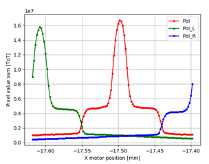
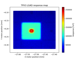
Figure 1 shows the response profile from the 110 $\mu m$ pixel device from the X-ray beam as the pixel array was moved relative to the beam for the pixel of interest (PoI), and its neighboring pixels (left-hand side and right-hand side pixels). The quantity plotted is the integrated time-over-threshold (ToT) for the pixel from an illumination of 5 seconds per illumination position. This corresponds to the total collected charge at the pixel electrode. The PoI boundaries can be seen between motor positions -17.55 and 17.44 mm. A region of gain in the middle of each pixel can clearly be observed. The gain of factor approximately three can be extracted directly from the pixel profile. Figure 2 shows a 2D map obtained by a raster scan of the pixel array recording the integrated ToT from the PoI. The regions of gain and no gain are clearly visualized. Results obtained suggest a good degree of understanding of the fabrication processes involved but demonstrated the limitations of the standard LGAD process with a JTE for small pixel. This work will report on the characterisation of fabricated devices and suggest mechanisms for mitigating the effects of limited gain regions for small sized pixel.