Choose timezone
Your profile timezone:
Registration
A registration fee of 120 Euros will be charged to participants attending in-person the Workshop. Online attendance is also possible (free of charge). A double registration is required for in-person participants: here in indico, while the payment is managed by the ADEIT.
A link to connect online to the Workshop will be provided to participants.
The in-person workshop will be held at the ADEIT conference centre located at the heart of Valencia city.
The registration is a 2 step process:
1) Indico registration for all the participants (online and in-person),
2) Payment via the ADEIT Organization (via Credit Card or Bank Transfer) for in-person participants. Your registration will not be completed until the payment form is filled out as well. The online payment form must be completed in addition to indico form at ADEIT webpage :
Travel, accommodation and additional information
Useful information about the travel, accommodation, venue and some other additional information can be found under the tab Local information.
Videoconference information
All the information required to connect online to the Workshop sessions is under the tab Videoconference information (access restricted to registered persons).
 |
 |
 |
|
|
 |
 |
Wide band gap semiconductors, such as GaN and SiC, have exhibited notable advantages, when they are applied as a nuclear radiation detector in a harsh environment of high temperature or strong radiation field. Recently a GaN alpha-particle detector of p-i-n structure was fabricated on a sapphire substrate in this article. The intrinsic layer of the detector was isoelectronic Al-doped GaN with the thickness of 10 µm. The leakage current of the detector remained below 10 pA when the reverse voltage increased from 0 to 40 V, which proved that it had a better crystal quality than the detector based on undoped i-GaN layer, of which the dark current was 10 nA at −40 V. The i-GaN layer would be fully depleted at −48 V. With the remarkable improvement of electrical properties, the charge collection efficiency (CCE) of the full depleted detector in this article was as high as 99%, while the energy resolution was about 4%. Further, in order to obtain better time resolution characteristics, the 3D SiC detector was developed using a laser drilling method. The SiC single crystal was about 350 microns, and the diameter of the holes are 50 microns and 100 microns, respectively. Then Indium was filled into the holes. The basic electrical characteristics have been mastered by I-V and C-V tests.
SiC as a typical wide bandgap semiconductor material has the potential to be used in the high energy field thanks to its good performance under radiation environment as well as running without cooling compared with traditional Si devices. Followed by the previous study of the timing performance of the 4H-SiC PIN device, a first 4H-SiC LGAD has been fabricated by Nanjing University (NJU) China. The device has 20µm active layer and 0.15µm gain layer. The preliminary test results of the electrical properties and response from alpha particle will be presented.
The Non Ionizing Energy Loss (NIEL) concept is used to compare and scale the damage impacted on semiconductor devices in different radiation fields. A particular weakness of the present NIEL concept consists in the inability to predict the different formation rates of cluster and point defects in the silicon (Si) crystal for different particles and particle energies. NIEL gives only the total energy imparted in displacements and does not separate between energy going in point defect formation and energy going into cluster formation. To be more specific, differences between radiation damage produced by neutrons and protons of the same displacement energies (i.e. damage parameters normalized to the NIEL) has been observed experimentally. In this work, we present the results of Geant4 and FLUKA simulations in order to investigate proton/neutron differences from first principles. The interactions of neutrons and protons of different energies in a 100 um thick Si target were studied and the kinematics of the Primary Knock-on Atoms (PKA) has been characterized. The dependence on NIEL on the target recoil energy is explored along with its dependence on secondary particle production from inelastic collisions.
We report on results of the irradiation bulk damage study in gamma irradiated standard float zone p-type silicon diodes. The study includes three types of diodes with different resistivities by CNM, HPK and IFX manufactures. The diodes were irradiated by Cobalt-60 gamma source up to 3.66 MGy in approximate charged particle equilibrium and then annealed for 80 minutes at 60°C. Electrical properties of diodes are characterized by measuring IV and CV curves of each diode before and after irradiation and annealing. During all the measurements we were able to separate surface and bulk currents by contacting the guard ring of each diode. The measurements of n-in-p type diodes show increasing linear-looking dependence of leakage current and decreasing linear-looking dependence of full depletion voltage and effective doping concentration on TID.
This project focuses on the investigation of trap energy levels introduced by radiation damage in epitaxial p-type silicon. Using 6-inch wafers of various boron doping concentrations (1e13, 1e14, 1e15, 1e16, and 1e17 cm-3) with a 50µm epitaxial layer, multiple iterations of test structures consisting of Schottky and pn-junction diodes of different sizes and flavours are being fabricated at RAL and Carleton University.
In this talk, details on the latest iterations of diode fabrication on high and low-resistivity wafers and electrical measurements of the structures will be given. IV and CV scans of fabricated test structures have been performed and cross-checked between institutes, the results of which will be presented. Emphasis will be placed on approaches to reduce the surface component of the leakage current that could potentially be applicable to the foreseen irradiated sample measurements.
Furthermore, process and electrical simulations of the diodes fabricated from the high resistivity wafer will be shown.
Finally, the on-going activities for charge collection measurements, the next round of wafer processing, and proposed plans for irradiation in the coming months, will be reviewed.
The operation of Low Gain Avalanche Detectors (LGADs) in the harsh radiation environment of the CERN-LHC is limited by the disappearance of the gain at particle fluences higher than 2E+15 cm-2 due to the so-called Acceptor Removal Effect (ARE). Thereby radiation induced defects inside the highly doped LGAD multiplication layer are created, like the boron-interstitial oxygen-interstitial (BiOi), that deactivate the active boron dopant and reduce the capability for charge multiplication. However, based on fundamental defect models, BiOi formation alone does not explain the observed ARE in the highly B-doped LGAD layer. Here we present defects characterization studies on LGADs using Deep-Level-Transient-Spectroscopy (DLTS) as well as Thermally Stimulated Current technique (TSC). Besides an overview about defects that were created, we will also discuss limitations of the characterization techniques applied to LGADs caused by e.g. charge multiplication effects, device geometries as well as internal defect induced electric fields.
In this work the Thermally Stimulated Techniques including TS-Current (TSC) and TS-Capacitance (TS-Cap) has been used to study the properties of the radiation induced BiOi defect complex by 6 MeV electrons. Two different types of diodes manufactured on p-types epitaxial-(EPI) and czochralski-CZ silicon with a resistivity of about 10 Wcm were irradiated with fluence values in the range between 1 x 1015 cm-2 and 6 x 1015 cm-2. In order to evaluate the parameter of BiOi defect (activation energy, capture cross section, concentration) from the TSC and TS-Cap measurements the well known electric field enhance emission effect (Poole Frenkel effect) in 3D version had to be considered and was included in the simulation software. The changes of the position dependent electric field strength, the effective doping profile as well as the occupation of the defect during the BiOi emission were simulated as function of temperature in the relevant range. In addition, the macroscopic properties (dark current and effective doping concentration) were extracted from current-voltage (I-V) and capacitance-voltage (C-V) measurements at 20oC for the EPI- and Cz-diodes. Furthermore, isothermal annealing studies at 80oC for annealing times between 0 min and 120 min had been performed. The results will be presented and discussed.
Charge collection in Si p+-n-n+ detectors was studied in the in situ irradiation test at 1.9 K with intense 23 GeV proton beam fragmented in 400 ms spills in view of detector application as beam loss monitors in the LHC at CERN. The current pulse responses demonstrated a two-stage process of charge collection, in which, in the first stage, the current was induced by holes, and in the second, by electrons arising due to avalanche multiplication produced by holes. The data treatment and the current response shapes simulation for detectors irradiated by 51013 p/cm2 yielded a full set of carrier transport characteristics and a signal internal gain. The charge collected in the second phase exposed a threshold in voltage for the signal rise, which verifies evolution of avalanche multiplication as the origin of the second phase and total signal amplification. In Si detector irradiated to 2.71014 p/cm2, a new third stage of charge collection was observed and assigned to avalanche multiplication produced by electrons reaching the n+ contact and to the following drift of generated holes back to the p+ contact.
Gordana Lastovicka-Medin1, Mateusz Rebarz2, Gregor Kramberger3, Jakob Andreasson2 Tomas Lastovicka4, Jiri Kroll4, Kamil Kropielnicki2
1University of Montenegro
2Extreme Light Infrastructure
3Jozef Stefan Institute
4Czech Academy of Sciences
Different active thickness of LGADs and probing the sensitive depth from front and backside are exploited, The sensors used in this study are as follows: BK UFSD3.2 W18 with C-enriched gain layer and with active thickness of 47 microns (2x2 array); HPK-P2 W36 (no C-enriched gain layer) with 50 microns of active thickness, 2x2 area); HPK-P1, Type 1.2 , 35 microns and CNM - sensor from Run9254 with active thickness of 70 microns. All types of sensors are irradiated at the fluence of 1.5e15 and 2,,5e15 neq/cm2. Femtosecond laser based SPA mortality study was manly focused on study of LGAD's stability because we tried to avoid fatal damage so that sensors can be subjected to the illuminated from the back side. Front illumination was performed on all considered sensors sensors. TPA mortality study was performed from both sides: front and back. The results are discussed as well as future plans,
Gordana Lastovicka-Medin1 , Milko Jaksic2 , Gregor Kramberger3 , Mauricio Rodriguez Ramos2 , Andreo Crnjac2 , Milos Manojlovic1
1 University of Montenegro,
2 Rudjer Boskovic Institute,
3 Jozef Stefan Institute
This work in progress is three folded. Firstly, gain anomalous behavior was studied in a such way that ion beams (C, He, Li, H+) and their energies were chosen so that Bragg peaks correspond to the same depth in LGAD but significantly different charge was deposited. Secondly, protons of 4 MeV energy were used to irradiate LGAD from two sides: back and front. The aim was to systematically observe the contributions of impact ionization and multiplication of holes and electrons in more distinguishable way, knowing at the same time the most probable depth where induced charge should be mostly generated. However, since slowing down of ions in matter is accompanied by a spread of beam energy, this so called energy straggling effect has to be studied in depth. The difference in energy lost when 4 MeV H+ ion is injected from front and back side is considered too. Thirdly, intrepid distance vs bias was mapped using probing H+ ion beams: 0.75, 1,15 and 1,5 MeV.
Degradation of semiconductor detectors when exposed to high radiation rates leads to the necessity of development of tools and methods for characterization of these devices. One of these methods is the Two-Photon Absorption – Transient Current Technique (TPA-TCT) which provides spatially-resolved inspection of semiconductor detectors. This technique exploits the simultaneous absorption of two photons of same energy. Said energy being lower than the band-gap energy of the semiconductor material and higher than half the band-gap energy. The photons are delivered by a femtosecond laser and the absorption occurs only at the focal point of the laser beam focusing optics, allowing localized generation of transient current. In order to avoid single-photon absorption when performing TPA-TCT on silicon detectors, emission wavelengths longer than 1150 nm are required.
Mode-locked Ti:Sa solid state lasers are the current standard optical source of femtosecond pulses. Their natural emission wavelength is out of the 1550 nm region and complex and expensive conversion techniques are required to extend it. Instead, erbium doped fiber laser emission lies naturally in that region. This is why we recently developed a femtosecond fiber laser system of properties and functionalities particularly designed for the TPA-TCT. Said system was based in an all-fiber chirped pulsed amplification architecture seeded by a solitonic passively mode-locked erbium doped fiber oscillator, where the properties of the output pulses from said architecture were configured arbitrarily by free space optics accessories. These accessories allowed selection of pulse energy from < 10 pJ to > 10 nJ, pulse repetition rate from single shot to 8 MHz and pulse duration from 300 fs to 600 fs.
Our current work aims to achieve all these configurable properties through a fully all-fiber system to offer improved robustness and efficiency, while maintaining the required levels of average power and temporal coherence. We are doing this as follows: firstly, the stretching stage will be based in a chirped fiber Bragg grating of tunable dispersion, which will allow the variation of the pulse duration at the output of the source. Secondly, a fiber-pigtailed acousto-optic modulator will be designed and implemented in the system to perform, all-in-one device, the following functionalities: pulse energy selection, pulse repetition rate tunability and emission-to-detection synchronization.
The Two Photon Absorption – Transient Current Technique (TPA-TCT) uses fs-pulsed infrared lasers, with photon energies below the silicon band gap. Excess charge carriers are generated mainly in a small volume (approximately 1µm × 1µm × 20µm) around the focal point of the laser beam, enabling resolution in all three spatial directions. Following the initial success of the method, a compact TPA-TCT setup was developed at CERN. The current setup status, first measurements on LGAD sensors with focus on the gain suppression mechanism, measurements on non-irradiated PIN diodes, and Single Event Effect (SEE) studies in a RD53B chip will be presented.
We present the commissioning measurements of the new fiber femto-laser at IFCA equipped with a fully integrated optical bench for microfocusing, signal stability monitoring and focus imaging. Compensation of the TPA-TCT signal fluctuations using the second harmonic generated with a BBO crystal will be described
TCT was used to study the effect of ionization density on gain in different non-irradiated LGADs. A simple model was used to explain the screening and was verified by measurements.
Existing impact ionisation models and parameters for silicon do not accurately describe the behaviour seen in LGAD sensors, so new impact ionisation parameters specifically applicable to LGADs was determined using simulations and timing measurements of sensors from various producers. The resulting model and parameters will be presented.
Access to the Collaboration Board meeting session through the following link:
https://indico.cern.ch/event/1096752/
In this contribution, I will discuss two possible evolutions of the LGAD design.
DC-RSD: up to now, resistive read-out in silicon detectors has been used only in AC-coupled detectors, the so-called AC-RSD or AC-LGAD. I will present here the first attempt to apply resistive read-out to a DC-coupled sensor.
LGAD with bias ring: recent beam tests results showed that LGADs suffer destructive break-down if the field in the bulk is above 11V/um. SiPMs manage to survive similar conditions given the presence of quenching resistors. I will present a possible LGAD design that introduces AC-coupled read-out and quenching resistors in each pad. This design should also provide increased stability with respect to floating pads or pads with high currents.
The High Granularity Timing Detector (HGTD) project of ATLAS will reduce the pile-up effect in HL-LHC by providing precise time measurement of tracks. The Low- Gain Avalanche Detector (LGAD) with time resolution better than 35(70) ps before(after) irradiation is the key technology which has been studied by many institutes. The Institute of High Energy Physics Chinese Academy of Science (IHEP) has been developing LGAD sensors IHEP-IME with the Institute of Microelectronics of the Chinese Academy of Sciences (IME). So far two versions of IHEP-IME LGAD sensors has been produced, IHEP-IMEv1 and IHEP-IMEv2. IHEP-IMEv1 sensors showed good potential in achieving the HGTD requirements with time resolution better than 60 ps and 4 fC charge collection around 700 V after irradiation. IHEP-IMEv2 sensors have modified doping profile compared with last version, especially focusing on the carbon implantation effect. Sensors with diverse producing process and carbon dose were fabricated and have showed improved performance. This talk will present the test results of IHEP-IMEv2 sensors irradiated with fluences of 0.8 ×10¹⁵ neq/cm2, 1.5 ×10¹⁵ neq/cm2 and 2.5×10 neq/cm2 and compare them with results before irradiation. After irradiation, sensors with different carbon dose showed different performance. The effect of carbon implantation will be shown. Low temperature beta test results showed that, after 2.5×10 neq/cm2 irradiation sensors collect 4 fC at less than 400 V with time resolution better than 50 ps, by far satisfying the requirements.
To suppress the pile-up expected at High-Luminosity LHC, timing information can be assigned to particle tracks. In order to implement this technique, track timing resolution of the order of tens of picoseconds is required over the lifetime of the detector. Low Gain Avalanche Detectors (LGADs) were selected as the basis for the timing detectors at the HL-LHC, offering suitable timing resolution. While the development and testing of sensors is undertaken by the University of Oxford, the University of Birmingham, the Rutherford Appleton Laboratory, and the Open University, production of LGAD sensors is done by Teledyne e2v. This collaboration focuses on developing ultra-fast silicon detectors with characteristics suitable for the implementation in the HL-LHC High Granularity Timing Detector, with the potential to be used in other high-energy experiments as well. In this talk we will present results from one of the LGAD wafers produced by Teledyne e2v, focusing on the measurements of charge collected and gain, including jitter measurements, using a system based on a ps laser source and SPICE characterization of the RF amplifiers used. Details and plans for future tests will also be discussed.
The University of Birmingham, University of Oxford, the Rutherford Appleton Laboratory and the Open University are developing and testing new LGAD sensors. This project, aims at developing Ultra-Fast Silicon Detectors (UFSD) of characteristics and performance suitable for use at HL-LHC High Granularity Timing Detectors (HGTDs) in collaboration with a company having significant long-standing production capabilities for scientific imaging sensors, Teledyne e2v Ltd.
The first fabricated batch of 22 six-inch wafers, featuring 50 µm thick high resistivity epi layer with different gain layer implants was completed successfully and I-V and C-V characteristics presented previously to RD50. Here we discuss the commissioning of the Strontium-90 source set-up and first measurements of timing resolution with these LGADs which are already in the 30ps range. We also discuss some improvements to our laser TCT setup with additional gain measurements. Lastly we present the plans for further improvements to the timing system and testing of devices after proton irradiation at the MC40 facility.
Motivated by the need for fast timing detectors to withstand up to 2 MGy of ionizing dose at the High Luminosity Large Hadron Collider, prototype low gain avalanche detectors (LGADs) have been fabricated in single pad configuration, 2x2 arrays, and related PIN diodes, and exposed to Co-60 sources for study. Devices were fabricated with a range of dopant layer concentrations and, for the arrays, a variety of inter-pad distances and distances from the active area to the edge. Measurements of capacitance versus voltage and leakage current versus voltage have been made to compare pre- and post-irradiation characteristics in gain layer depletion voltage, full bulk depletion voltage, and breakdown voltage. Conclusions are drawn regarding the effects of the gammas both on surface and interface states and on their contribution to acceptor removal through non-ionizing energy loss from Compton electrons or photoelectrons. Comparison of the performances of members of the set of devices can be used to optimize gain layer parameters.
Low Gain Avalanche Detectors (LGADs) are a promising technology for high energy physics experiments, since they can potentially offer spatial resolution down to sub $100$ $\mu m$ and temporal resolution below $100$ $ps$ simultaneously. Thanks to these properties, these devices are considered for the upgrades of the ATLAS, CMS, and LHCb experiment at CERN.
This work will focus on timing resolution studies of recent devices produced by the University of Glasgow and Micron Semiconductor Ltd. These devices will be compared to those produced at CNM Barcelona. Specifically, details of the produced devices will be introduced and the Sr-90 experimental setup to measure the timing resolution will be described. Time resolution for Micron-Glasgow devices in the region of $55$ $ps$ was achieved. Specifically, the measurement results for both CNM and Micron-Glasgow devices show temperature and bias voltage dependence of timing resolution and the details will be discussed. Finally, the outlook for future developments and studies will be presented.
In this contribution, we will present measurements on
neutron-irradiated LGADs corresponding to our 6-inch, 50µm active
layer thick, epitaxial wafers run (6LG3). Samples were fabricated
using three boron implantation doses, and one energy, for the gain
layer definition. Gain, collected charge, acceptor removal constant
and timing measurements were carried out on these LGADs irradiated
with neutrons at equivalent fluencies ranging from 1e14 to 5e15
atm/cm2. The presented results have served as a stepping stone to
select the best technological parameters for the gain layer definition
in the upcoming ATLAS-CMS common runs, based on 6-inch epitaxial and
Si-Si wafers (6LG3 and 6LG2 technologies, respectively).
The fast rising signal of LGADs with high signal-to-noise ratio is key to achieve an excellent charge collection and time resolution for Minimum Ionizing Particles (MIPs). The LGAD technology will be used for the HL-LHC in the upgrade of both ATLAS and CMS timing detectors.
A full characterization of CNM LGADs on Si-Si and low resistivity epitaxial wafers irradiated up to 1e16 neq/cm2 will be presented. LGADs are first electrically characterized on probe stations at room and at cold temperature. From the IV and CV characteristics parameters such as leakage current, full and gain layer depletion and breakdown voltages are studied. The rate of self pulses without an external source is measured to determine the maximum operational voltage. Measurements with a Sr-90 radioactive source are performed to study charge collection and timing from MIPs. Other parameters such as noise, jitter and rise time have been studied. The collected charge and time resolution performance is also studied at different bandwidths to understand how these parameters could be eventually affected by the readout.
Trench-Isolated LGAD (TI-LGAD) is a novel LGAD design where the standard inter-pixel isolating structure has been replaced with a trench, physically etched in the silicon and filled with a dielectric material.
The "RD50 TI-LGAD" project aimed at exploiting this new technology for the production of pixelated detectors with pixel and strip pitches down to 50 µm.
In the project framework, FBK produced a batch of TI-LGADs, where many different technological and layout splits have been tested. In this contribution, we will present the parametric and functional characterization of the produced samples and discuss the following characterization activities that will be carried out by the partner institutes.
We present a characterization of the novel Trench-Isolated LGAD (TI-LGAD) technology using a scanning TCT setup. The studied devices belong to the first production of pixelated TI-LGADs at FBK done in the framework of the RD50 collaboration. The TI-LGAD is a variation of the Low-Gain Avalanche Detector (LGAD) in which the segmentation of the detector in pixels is done by etching physical trenches that isolate each pixel. TI-LGADs display the same outstanding performance of LGADs in terms of time resolution, while at the same time allow for a smaller inter-pixel distance, thereby increasing the fill factor, which is a requirement for pixelated LGADs that can provide both precision timing and position resolution (4D pixels). Several structures have been tested before irradiation using a TCT-setup at UZH. A comparison between the results from the different design patterns (number of trenches, depth of trenches, etc.) in this production will be discussed. The plan for an irradiation campaign will be presented.
The Flavor physics program is one of the important topics for future lepton collider projects. In order to explore the full potential of the flavor physics program, a time-of-flight detector is needed to perform particle identification at an energy range from 1GeV to 5GeV.
We propose a time-of-flight detector based on AC-coupled LGAD technology, which has high timing resolution and spatial resolution. It can serve as a time-of-flight detector and outer layer of the tracking detector.
The Institute of High Energy Physics Chinese Academy of Science (IHEP) developed a prototype of AC-coupled LGAD detector. According to the laser test results, it can reach 5-10 microns spatial resolution using 2*2 AC pads array design with a millimeter level pitch. The spatial resolution and charge sharing effect have been studied with different n+ doping.
AC-coupled LGADs, also referred to as resistive silicon detectors (RSDs), rely on a design in which the multiplication layer and n$^{+}$ contact are continuous, and only the metal layer is patterned. In AC-LGADs, the signal is capacitively coupled from the continuous, resistive n$^{+}$ layer over a dielectric to the metal electrodes. The spatial resolution is not only influenced by the electrode pitch, but also the relative size of the metal electrodes. Knowledge of the capacitances of various sensor regions is crucial for understanding charge sharing in the detector, and for providing input for the design of suitable readout electronics.
We have studied the capacitances of the DC and AC contacts, interpad capacitances, and capacitance of the dielectric between the resistive n$^{+}$ layer and top contacts, using AC-LGADs both in small pad array and strip geometries. The impact of measurement parameters, such as serial or parallel mode, grounding of neighboring pads, and frequency will be discussed, while the role of metal electrode size and pitch, as well as n$^{+}$ layer doping, on the detector characteristics is investigated.
In this contribution we present RSD2, the second production of Resistive AC-Coupled Silicon Detectors (RSD), a new frontier in 4D particle tracking through Silicon detectors with internal gain and 100% fill-factor. RSD are n-in-p LGAD-based detectors characterized by three key-elements: (i) a continuous multiplication implant, without any segmentation, (ii) a resistive n-cathode and (iii) a dielectric coupling layer deposited on top. Thanks to the internal gain and the capacitive radout, RSD allow to reach almost the same timing performances of traditional LGADs, with high performances in space reconstruction. Starting from the very good results of the previous run, RSD1, we will introduce some important details about the new technological and physical parameters implemented in RSD2, designed at INFN Torino and manufactured in 2021 by Fondazione Bruno Kessler (FBK) in Trento. To this aim, TCAD simulations, layout design and a full electrical characterizations will be provided.
In this contribution, we present a new development of radiation-resistant silicon sensors. This innovative sensor design exploits the recently observed saturation of radiation damage effects on silicon, together with the usage of thin substrates, intrinsically less affected by radiation. The internal multiplication of the charge carriers will be used to overcome the small signals coming from thin substrates.
At the end of 2020, the Fondazione Bruno Kessler (Italy) delivered Low-Gain Avalanche Diodes (LGAD) produced on 25 and 35 $\mu$m thick p-type epitaxial substrates, namely the EXFLU0 production: I-V and C-V characterisation of the sensors has been performed before and after irradiation up to 1E17 n$_{eq}$/cm$^2$, together with signal analysis from an infrared laser stimulus.
The outcome of the laboratory tests and the device-level simulations will be implemented in the EXFLU1 production, in which optimisation of the sensor peripheries and the gain layer responsible for internal multiplication will be pursued. The goal is to pave the way for a new design of silicon sensors that can efficiently operate above fluences of n$_{eq}$/cm$^2$.
The development of detectors that provide high resolution in four dimensions has attracted wide-spread interest in the scientific community for several applications in high-energy physics, nuclear physics, medical imaging, mass spectroscopy as well as quantum information. The Low-Gain Avalanche Diode (LGAD) silicon technology has already shown excellent timing performances, but since fine pixelization of LGADs is difficult to achieve, the AC-coupled LGAD (AC-LGAD) approach was introduced to provide high spatial resolution. In this type of device, the signal is capacitively induced on fine-pitched electrodes placed over an insulator and is shared among multiple electrodes. AC-LGADs are therefore considered as promising candidates for future detectors to provide 4-dimensional measurements with high resolution in both space and time dimensions. AC-LGAD sensors designed and fabricated at the Brookhaven National Laboratory have been assembled and read out with a fast-time ASIC prototype, the ATLAS LGAD Timing Integrated Read-Out Chip (ALTIROC) that was developed by Omega/IJCLab for the ATLAS timing detector at the HL-LHC. The response of an AC-LGAD strip sensor to beta particles and infra-red photons has been measured using an ALTIROC ASIC prototype. The presentation will include studies of signal sharing between electrodes, as well as spatial and time resolution.
We present measurements of AC-LGADs performed at Fermilab’s test beam facility using 120 GeV protons. We studied the performance of various strip and pixel sensors that were produced by BNL and HPK. The measurements are performed with our upgraded test beam setup that utilizes a high precision telescope tracker, and a simultaneous readout of up 6 channels per sensor, which allows detailed studies of charge sharing characteristics. These measurements allow us to assess the differences in designs between different manufacturers and optimize them, based on experimental performance in test-beams. We then study several reconstruction algorithms to optimize position and time resolutions that utilize the charge sharing properties of each sensor.
We analyzed beam test data from a beam test at FNAL with 120 GeV protons to show the effect of signal sharing in AC-LGAD fabricated by BNL and FBK. The main thrust is the understanding of the signals underneath the metal pads/strips which can’t be investigated with laser light which is usually used.
The two topics discussed are the position resolution and the long-range pulse sharing.
Achieving granularity below the 1 mm scale (100 um or less) while maintaining high efficiency, precise timing, and good spatial resolution is a goal of continued R&D on silicon diode Low Gain Avalanche Detectors (LGADs). One approach, proposed by the SCIPP ultrafast sensor R&D group, is to make use of the diode junction to create avalanche-generating fields within the sensor, and then to bury the junction underneath several microns of n+ material to keep surface fields low, and allow for conventional pixelization techniques. In this talk, we will remind the audience of the principles of operation of the Deep Junction LGAD, and present updates relating to its design and fabrication.
The AC-LGAD technology has been shown to be a very promising technology within HEP due to it's extremely good time resolution and 100% fill factor. This technology is proposed to be used with the Timepix4 ASIC for imaging applications using soft X-rays. The fabrication of these devices is underway. Simulation studies have been performed to optimize the technology for a 55um pixel pitch and a radiation damage study has been performed in order to understand the performance of these devices within HEP experiments and to study the surface damage effects for soft-x-ray detection.
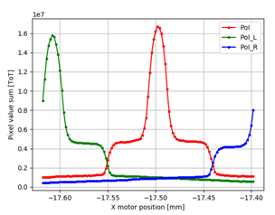
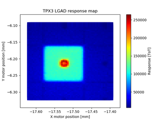
In this work the properties of 200 $\mu m$ thick highly pixelated LGAD sensors bonded to a Timepix3 readout ASIC were characterised for the first time. Recent advances in the control of the LGAD fabrication process by Micron Semiconductor Ltd has allowed the manufacture of highly segmented devices where each pixel has an internal gain. Devices with 55 $\mu m$ pixel with 5 $\mu m$ Junction Termination Element (JTE), 110 $\mu m$ pixel with 10 $\mu m$ JTE and 110 $\mu m$ pixel with 20 $\mu m$ JTE where bump bonded to a Timepix3 readout ASIC and characterised with a micro-focus monochromatic 15 keV X-ray beam.
Figure 1 shows the response profile from the 110 $\mu m$ pixel device from the X-ray beam as the pixel array was moved relative to the beam for the pixel of interest (PoI), and its neighboring pixels (left-hand side and right-hand side pixels). The quantity plotted is the integrated time-over-threshold (ToT) for the pixel from an illumination of 5 seconds per illumination position. This corresponds to the total collected charge at the pixel electrode. The PoI boundaries can be seen between motor positions -17.55 and 17.44 mm. A region of gain in the middle of each pixel can clearly be observed. The gain of factor approximately three can be extracted directly from the pixel profile. Figure 2 shows a 2D map obtained by a raster scan of the pixel array recording the integrated ToT from the PoI. The regions of gain and no gain are clearly visualized. Results obtained suggest a good degree of understanding of the fabrication processes involved but demonstrated the limitations of the standard LGAD process with a JTE for small pixel. This work will report on the characterisation of fabricated devices and suggest mechanisms for mitigating the effects of limited gain regions for small sized pixel.
Where we present the characterization of the HVCMOS MPW2 chip pixel matrix using the ion microprobe station at the RBI 1 MV Tandetron accelerator with protons at 2 MeV. The proton beam spot (most probable area of impact) was around 30 um2, small enough to scan pixel by pixel the whole pixel matrix and with energy low enough to avoid SEE effects.
In high energy physics, the silicon pixel sensors manufactured in commercial CMOS chip fabrication lines have been proven to have a good radiation hardness and spatial resolution. Along with the mature manufacturing techniques and the potential of large throughput provided by the foundries, the so called "passive CMOS" sensor has become an interesting alternative to standard planer sensors.
High and predictable breakdown behaviour is a major design goal for sensors and the guard-ring structure is one factor to optimise. This is especially important for the applications that require higher voltages.
We present a concept of the guard-ring design which can be realised in the LFoundry 150nm CMOS technology. Indicated by TCAD simulations, such design can lead to a higher breakdown voltage by modifying the potential and electric field distribution in the guard-ring area. A number of test-structures have been designed for the RD50-MPW3 submission for verifications and further studies.
Passive CMOS pixel sensors are investigated in the context of the CMS Phase2 Tracker Upgrade. A prototype production of RD53A compatible pixel sensors was recently completed at LFoundry in 150nm CMOS process. This presentation will focus on the characterization of irradiated and non-irradiated pixel modules, composed by a CMOS passive sensor interconnected to a RD53A chip. The sensors are designed with a pixel cell of 25 um ×100 um in case of DC coupled devices and 50 um ×50 um for the AC coupled ones. Their performance in terms of charge collection, position resolution, and hit efficiency was studied with measurements performed in the laboratory and with beam tests. The RD53A modules with LFoundry silicon sensors were irradiated to fluences up to 2x10**16 neq/cm2.
The new ATLAS Inner Tracker (ITk) sub-detector is necessitated by the impending High Luminosity Large Hadron Collider (HL-LHC) upgrade. This replacement is part of the phase-II upgrade programme for the HL-LHC which will see a sevenfold increase in peak instantaneous luminosity with a total ionizing dose of 53 MRad. The fully solid state ITk will employ silicon n+-in-p microstrip sensors in the outer layers of the tracking detector. The main sensors are manufactured on 6” diameter silicon wafers. Periphery wafer area (halfmoons) to which the main sensor does not extend serves as convenient venues for the implementation of test devices. The primary utility of the test devices is Quality Assurance (QA), that is, the monitoring of the consistency and reliability of the manufacturing process. A Metal-Oxide-Semiconductor (MOS) and Gate-Controlled Diode (GCD) are two such test devices aimed at characterizing the surface oxide and silicon-oxide interface. Measurement procedures and parameters for QA are established for these devices and the viability of these tests for gamma irradiated samples is evaluated. The suitability of these devices to further monitor the strip sensor fabrication process is also investigated.
We report on the measurements of time resolution for double-sided 3D pixel sensors with a single cell of 50 $\mu$m $\times$ 50 $\mu$m and thickness of 285 $\mu$m, fabricated at IMB-CNM and irradiated with reactor neutrons from 8e14 MeV n$_{eq}$/cm$^2$ to 1.0e16 MeV n$_{eq}$/cm$^2$.
Measurements were conducted using a radioactive source at a temperature of $-$20 and 20 \textdegree C in a bias voltage range of 50-250 V. The reference time was provided by an LGAD detector produced by Hamamatsu. The results obtained are compared to measurements conducted prior to irradiation.
The next generation of inner tracking detectors will require spatial resolution down to 10um, radiation hardness above 10e16Neq/cm^2 together with a temporal resolution in the order to tens of pico seconds.
To face these challenges and overcome limitations of today's technologies, an alternative approach to internal gain through the use of a radiation sensitive doping layer is investigated and simulated. An enhanced radiation hardness is foreseen by implementing additional metallic structures in the sensor substrate. These can be biassed in such a way that localized high electric field are created. In this talk, TCAD and Garfield++ simulations of this proposed structure will be presented along with plans of fabrication. Gain in excess of a factor 10 can be acheived and the temporal response is similar to those of LGADs.
In this presentation the relation between the leakage current and full depletion voltage to TID will be shown. From the measured I-V and C-V characteristics it is obvious that the dependence of the leakage current with respect to the TID is increasing linearly. On the other hand, the full depletion voltage and thus also the effective doping concentration shows a decreasing trend with higher TID. This gradual decrease of the effective doping concentration could be interpreted as acceptor removal or donor introduction.
For the purpose of this study $14$ diodes fabricated together with the main ATLAS pre-production sensors on n-in-p standard float zone silicon wafers with the initial resistivity of about $3\,\mathrm{k\Omega} \cdot \mathrm{cm}$ were irradiated by ${}^{60}$Co gamma rays up to a total dose of $366\,\mathrm{MRad}$ in approximate charge particle equilibrium. The samples consist of several test structures including $8\times 8\,\mathrm{mm}^2$ diodes which enables the study of leakage current and bulk capacitance. The advantage of using these diodes is the presence of contact pads on the guard ring which allows it to be grounded during I-V and C-V measurements and thus makes it possible to separate the bulk and surface current. The samples were measured before irradiation and after gamma irradiation both before and after annealing.
The proton irradiation site at Bonn University has been introduced at previous RD50 workshops. Recently, the setup has been upgraded to minimize fluence fluctuations on the DUT and enable flexible irradiation procedures. The Bonn Isochronous Cyclotron delivers 14 MeV (~12.5 MeV on-device) protons with typical beam currents of 1 𝜇A and beam diameters of a few millimeters to the setup. Enhanced beam diagnostics as well as R/O electronics allow for online monitoring across several orders of magnitude of beam currents with a relative uncertainty of approx. 1%.
Devices are irradiated by being scanned through the beam in a row-wise pattern while housed in a thermally-insulated cooling box at approx. -20 °C to minimize annealing. Online monitoring of the beam current at extraction allows to measure the fluence per scanned row, ensuring homogeneous irradiation, with an accuracy of a few %. The setup allows to power and readout DUTs during irradiation as well as pause irradiations for in-between measurements. Latest irradiations of thin LFoundry test structures yield a proton hardness factor with reduced uncertainty, compatible with previous measurements and simulation, enabling to irradiate up to 10$^{16}$ n$_{eq}$/cm² within a few hours. The setup, its reworked components, the irradiation procedure as well as the latest proton hardness factor measurements are presented in this talk.
The CMS detector will be upgraded to face a 10-fold increase in integrated luminosity for the High-Luminosity LHC era. Its endcap calorimeters will be replaced by the high-granularity calorimeter (HGCAL). With its unprecedented transverse and longitudinal readout/trigger segmentation, with more than 6M readout channels, HGCAL will facilitate the use of particle-flow calorimetry. Silicon pad sensors will be used for high radiation regions, covering a total area of 620 m$^2$, where it is expected to reach integrated neutron fluences of $10^{16}$ neq/cm$^2$ and doses of 1.5 MGy. The silicon sensors are processed on 8-inch wafers with three different thicknesses (300, 200, 120 $\mu$m), and cut into hexagonal shape for tiling and for optimal use of the wafer area. Each sensor is segmented into several hundred cells of hexagonal shape of 0.5 to 1.1 cm$^2$ in size, each of which is read out individually. In addition to the main sensors, the full wafer hosts small sized test structures used for quality assurance and radiation-tolerance tests. The talk will focus on radiation-tolerance studies performed with the hexagonal 8-inch sensors irradiated to fluences up to 10$^{16}$ neq/cm$^2$ at the novel neutron irradiation facility at Rhode Island Nuclear Science Center (RINSC, US). Using the ARRAY system (a customised probe and switch card system), their electrical properties in terms of pad leakage currents and capacitances have been measured for the first time, after neutron irradiation both without and with additional beneficial annealing. We present the results of those measurements, hereby qualifying the RINSC neutron irradiation facility and showing that the measured electrical properties of the HGCAL silicon sensors after irradiation meet expectations.
The CMS detector will be upgraded to face a 10-fold increase in integrated luminosity for the High-Luminosity LHC era. Its endcap calorimeters will be replaced by the high-granularity calorimeter (HGCAL). With its unprecedented transverse and longitudinal readout/trigger segmentation, with more than 6M readout channels, HGCAL will facilitate the use of particle-flow calorimetry. Silicon pad sensors will be used for high radiation regions, covering a total area of 620 m2, where it is expected to reach integrated neutron fluences of 110^16 neq/cm^2 and doses of 1.5 MGy. The silicon sensors are processed on 8-inch wafers with three different thicknesses (300, 200, 120 μm), cut into hexagonal shape for tiling and for optimal use of the wafer area. Each sensor is segmented into several hundred cells of hexagonal shape of 0.5 to 1.1 cm2 in size, each of which is read out individually. In addition to the main sensors, the full wafer hosts small sized test structures used for quality assurance and radiation-hardness tests. We present the results of an ongoing radiation-tolerance testing program of the bulk material of HGCAL prototype silicon sensors that has been carried out with test structure diodes irradiated up to 10^16 neq/cm^2 in the JSI Ljubljana reactor. This talk will focus on the annealing behaviour of the bulk material. Results on the electrical characterisation in terms of capacitance and leakage current measurements will be presented as well as measurements of the charge collection efficiency using infrared TCT as a function of annealing time.