Choose timezone
Your profile timezone:

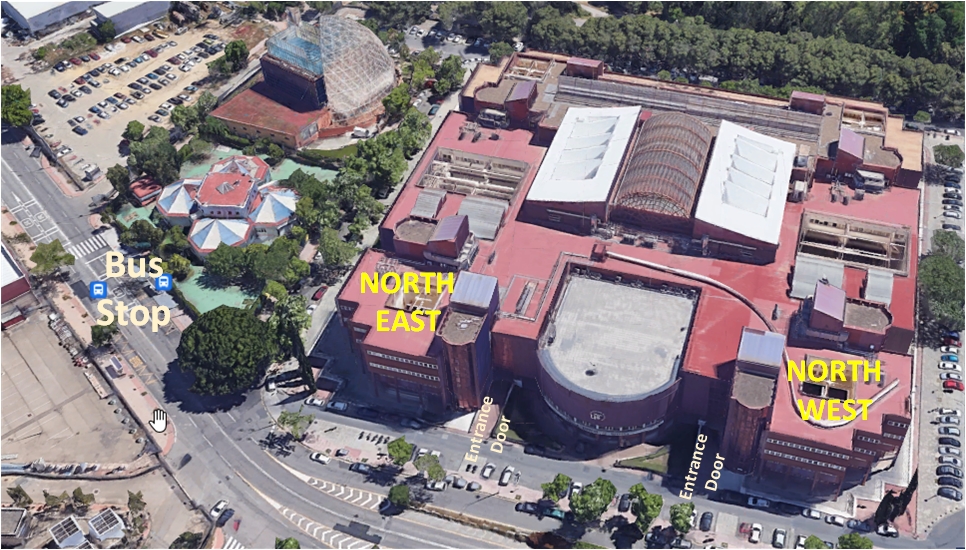
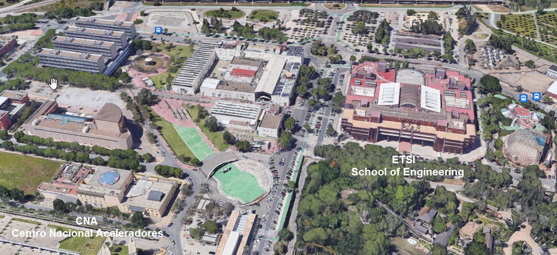
The in-person workshop will be held at the ETSI (Escuela Técnica Superior de Ingeniería, Technical School of Engineering, Camino de los Descubrimientos, Isla de la Cartuja) in Sevilla, Spain. The Collaboration Board meeting will be held at nearby CNA facility (Centro Nacional de Aceleradores, National Accelerators Center).
Visits to the National Center of Accelerators (Tuesday Afternoon):
There are 2 planned guided visits (up to 12 people each), free of cost, to the National Center of Accelerators, at walking distance from the School of Engineering. The visits are scheduled for Tuesday, during the celebration of the Collaboration Board (also at the National Center of Accelerators),
Tourist Visit to the Magallanes/Elcano Sites (Wednesday Evening):
Wednesday evening, starting at 18:30
Meeting Point: Torre del Oro, Sevilla
Two guides and audioguides for every participant
Recommendation, take the bus C1 towards the city centre:
C1 route towards Torre del Oro
Gala Dinner (Thursday Evening):
We will celebrate the Gala Dinner on Thursday Dec.1st evening at Hotel Los Seises, 20:30:
Travel, accommodation and additional information
Useful information about the travel, accommodation, venue and some other additional information can be found under the tabs Local information and Nearby Hotels.
Registration
Since November 14th registration is only possible for online participation. The in-person registration is closed since November 14th.
Indico registration for online participation:
Videoconference information
All the information required to connect online to the Workshop sessions is from the link (access restricted to registered persons):
 |  |  |
The Non-Ionizing Energy Loss (NIEL) concept compares and scales the damage impacted on semiconductor devices in different radiation fields. A particular weakness of the present NIEL concept consists in the inability to predict the different formation rates of cluster and point defects in the silicon (Si) crystal for different particles and particle energies. Specifically, differences between radiation damage produced by neutrons and protons of the same displacement energies (i.e. damage parameters
normalized to the NIEL) has been observed experimentally.
In this work atomic displacements in Silicon produced by high energy particles are studied. Neutrons, protons and electrons are defined as the initial beam in Geant4, the standard EM physics list is used and the resulting Primary Knocked-on atoms (PKA) are cross-compared with FLUKA simulation and saved. The PKA are then used as an input for another Geant4 simulation with a modified physics list containing ScreenedNuclearRecoil module and the resulting Silicon Cascade is saved. The OPTICS algorithm (Ordering points to identify the clustering structure) is then presented as a method of clustering. Further approaches towards tuning of the clustering algorithm is shown and electron induced damage is being suggested as a benchmark with actual measurements.
Carrier lifetime profiles, measured by diode (PIN and LGAD) edge scanning of microwave probed photoconductivity transients, are considered. The obtained carrier lifetime profiles are compared with the electrical (C V, I V) characteristics obtained on the same structures. It is shown that carrier lifetime variations correspond to the dopant density variations extracted using C-V characteristics within base region of the diodes. Additionally, the profiles of carrier recombination lifetime in structures irradiated by stopped protons are discussed.
This study is based on the IV, CV and CCE measurements of p-type Schottky diodes with 50 µm epitaxial layer to investigate the radiation bulk damage. Non-irradiated and various neutron irradiated (1e12, 1e13, 1e14, 1e15 and 1e16 [1MeV n_eq/cm^2]) diodes are being tested at RAL and Carleton University. Properties extracted from the measurements have been used in the TCAD simulations. In this talk, details of the procedure of the simulation will be given. And the comparisons of the simulations and the measurements will be presented.
Irradiation damages of the n-type silicon have been investigated for a long time, but not for the p-type silicon. This study is to investigate and improve the modeling and understanding of irradiation damage of epitaxial p-type silicon using Schottky diodes and pn junctions exposed to high neutron fluence up to 1e16 1 MeV n_eq/cm^2. This is a continuation of an ongoing project.
This talk will summarize and present the latest test results on IV, CV and CCE using lasers of the epitaxial p-type Schottky diodes and PN junctions. Description of improved test setup that allows the automatic scanning of the laser beam also at different temperatures of the samples will be given. Details of DLTS results on irradiated and non-irradiated devices will be given and differences between Schottky and PN junctions will also be highlighted.
Multistage impact ionization in Si detectors observed in the unique conditions of the in situ irradiation with 23 GeV proton beam fragmented into 400 ms spills and T = 1.9 K was analyzed using the current pulse responses of detectors irradiated to medium fluences. Within the range 5x10^13 - 2.7x10^14 p/cm2, the responses demonstrated two-stage and three-stage processes of charge collection, respectively, with sequential charge multiplication in the regions of high electric fields near both contacts. Data treatment allowed extracting the full set of carrier transport parameters, internal charge gain up to 3.7 and a significant rise in the hole trapping probability at 1.9 K in comparison with its value at T = -10˚C.
Boron-doped silicon detectors used in high radiation environment like the HL-LHC show a degradation in device performance due to the radiation induced deactivation of the active boron dopant. This effect is known as the so-called Acceptor Removal Effect (ARE) and depends on particle type, energy and radiation dose. Here we present defect characterization studies using TSC (Thermally Stimulated Current technique) and DLTS (Deep Level Transient Spectroscopy) on a set of epitaxial $^{60}$Co irradiated p-type Si diodes with two different resistivities (50 and 250 Ωcm). The irradiation dose was in the range of 100 kGy to 2 MGy. In our studies, we correlate radiation induced changes in the macroscopic device properties with the formation of microscopic defects. Furthermore, we used the defect parameters obtained by DLTS measurements for modelling the corresponding TSC spectra and compare them with our experimental results. This allows to open the discussion about the assignment of so far unspecified TSC peaks like the X-defect, to defect levels well identified in DLTS.
Two types of high resistivity p-type FZ diodes with p-stop and p-spray isolation between the pad and the guard ring were irradiated with 60Co gamma-rays. The dose values were 10, 20, 100, and 200 Mrad. In this work microscopic (TSC) as well as macroscopic (I-V, C-V) studies on isothermal heat treatments at 80 °C and isochronal annealing from 80 °C up to 300 °C were performed and analyzed for diodes irradiated to 100 and 200 Mrad. The results of these measurements will be presented. In addition, the unexpected frequency dependence of the C-V measurements in correlation with surface current measurements will be reported and discussed.
The effects of Fe-implantation on the electrical characteristics of Au/p-Si Schottky barrier diodes (SBD) were studied using current-voltage (I–V) and capacitance-voltage (C–V) techniques. The acquired results showed that the Si-based diodes were well fabricated, and Fe-implantation changed the normal diode's I-V behaviour from typical exponential to ohmic. The ohmic behaviour was described in terms of the defect levels induced by Fe that were positioned in the middle of the energy gap of Si. The C-V results show that Fe generates high density of minority carriers in p-Si which agrees with the increase in reverse current observed in I-V results. Also, the diode parameters in terms of saturation current, ideality factor, Schottky barrier height, doping density, and space charge region (SCR) width were used to investigate the effect of Fe in p-Si-based diode. Owing to the changes observed, which are analogous to those induced by dopants found to improve the radiation-hardness of silicon, it is safe to say that Fe can also assist in the quest to improve the radiation-hardness of silicon using defect-engineering method.
Silicon Microstrips detectors were considered as suitable for charge carrier mobility evaluation from magnetoresistivity (MR) phenomena. The top contacts geometry is potentially similar to Corbino disk, which is also used for MR with Hall electric field elimination. However, the appearance of negative MR caused by nonlinear electric field distribution prompted to search for alternative approaches including surface carrier excitation with light, modeling or the usage of bottom contact to translate direct current through the diode structure up to the linear response region. With completing more challenges related to geometrical factors, the detectors were evaluated after 1MeV neutron irradiation in the fluence range from $10^{15}$ to $10^{17}$ $cm^{-2}$. MR mobility and conductivity measurements enable to evaluate charge carrier density and the temperature dependency extracted thermal activation energy.
In this work we present 2D charge maps, CCE and timing measurements performed on 3D n-on-n silicon double sided 200µm thick sensors irradiated at different fluency levels, ranging from 1e14neq/cm2 to 1e17neq/cm2 on a TCT setup using different laser intensities, mimicking the height of the signal from a beta-source setup, and some multiples of it. We show CCE above 100% at 1E15neq/cm2 fluency due to charge multiplication while being 40% at the extreme high fluency of 1E17neq/cm2, and showcasing 200ps timing resolution up to 1e15neq/cm2 in very big diode arrays in which timing is highly limited by its noise due to a high capacitance.
Capacitance-voltage (CV) measurements are a widely used technique in
silicon detector physics. However, this only works if the sensor is not too heavily irradiated. After irradiation, the measured CV curves show strong frequency dependencies which is not the case before irradiation and thus, the derived parameters vary over a wide range, indicating that the method is not applicable for such devices. In this work, an existing, but not sufficient model for fitting CV measurements of irradiated sensors is extended. With this, the whole frequency range can be described. Unirradiated sensors produced by a CMOS foundry as well as irradiated CMOS, ATLAS R0 and ATLAS R5 sensors have been CV measured over the full, technically available, frequency range and were fitted with the derived model. Furthermore, it is investigated where the different frequency behaviour of the current CV analysis technique originates and it is shown how sensor parameters like the depletion voltage, the effective doping concentration and the bulk resistivity can be determined.
Signal reduction is the most important radiation damage effect on performance of
silicon tracking detectors in ATLAS. Adjusting sensor bias voltage and detection threshold can
help in mitigating the effects but it
is important to have simulated data that reproduce the evolution of performance with the
accumulation of luminosity, hence fluence.
ATLAS collaboration developed and implemented an algorithm that reproduces signal loss and
changes in Lorentz angle due to radiation damage. This algorithm is now the default for Run3
simulated events. In this talk the algorithm will be briefly presented and results
compared to first Run3 collision data.
For the high-luminosity phase of LHC (HL-LHC) a faster algorithm is necessary since the
increase of collision, event, track and hit rate imposes stringent constraints on the
computing resources that can be allocated for this purpose.
The philosophy of the new algorithm will be presented and the strategy on how to implement it
and the needed ingredients will be discussed.
Neutrons play a key role in many aspects of science and technology. Just to mention some examples, neutrons are responsible for the nucleosynthesis of elements in the stars or the functioning of fission and fusion reactors, but they are also a source of problems due when one considers the damage that they cause to, for instance, cells in radiotherapy cancer treatments or electronics devices in almost any environment, from flying airplanes to underground accelerator facilities. Therefore, neutron beams are needed for research in nuclear reactions, detectors tests, dosimetry, R2E, etc.
In Spain, the CNA HISPANOS facility in Seville is the only accelerator-based neutron beam facility. AT HISPANOS, neutrons with energies ranging from thermal (~25 meV) to fast (up to 10 MeV) are produced by means of 7Li(p,n), 2H(d,n) and 8Be(p/d,n) reactions. The beams can be continuous or bunched in pulses of only 2 ns, which allows for time-of-flight experiments or time resolved detector tests. The ion bean currents of a few uA provide fast neutron fluxes of about 1e9 n/s, reaching doses of ~1 Sv/h at at 30 cm from the target.
Access to HISPANOS is available free of charge through the Transnational Access projects H2020-ARIEL and H2020-EUROlabs.
https://indico.cern.ch/event/1204637/ (protected)
Silicon Carbide has interesting properties for high temperature, high radiation environment and timing radiation detector applications due to its thermal conductivity (3.7 W/(cm.°C)), atomic displacement threshold (22-35 eV) and high saturation velocity (2.2e7 cm/s). Silicon Carbide detector diodes have been fabricated in IMB-CNM with epitaxially-grown graphene onto Silicon Carbide (EG-SiC) as interface between the implant and the readout electrode, useful for e.g. heavy ion detection by removing metallisation in the active area. In this contribution, the effect of EG in a SiC PiN diode is studied as compared to a SiC sample without graphene by means of the Transient Current Technique.
4H-SiC devices could potentially operate in a harsh radiation and room-temperature environment because of its wider band gap, atomic displacement threshold energy and high thermal conductivity. We have simulated the IV, CV characteristics and gain efficiencies of 4H-SiC devices based on DEVSIM——an open source TCAD semiconductor device simulator. The reliability of the software can be verified by comparing the simulation results with the test results of the corresponding devices. In addition, in order to more accurately simulate the performance of 4H-SiC devices, we study the influence mechanism of non-ideal ohmic contact on the leakage current of the devices. Simultaneously, different defect types will have different effects on device performance. DEVSIM simulation can be used to identify harmful defects, thus reducing the formation of harmful defects.
Silicon carbide is a new type of semiconductor, and it is widely used in
optoelectronic devices, power electronic devices and other fields. Compared to
silicon semiconductor, silicon carbide has wider band gap, higher breakdown electric field, higher thermal conductivity and can stand greater irradiation.
We are planning to use silicon carbide device to make a proton beam monitoring system. We will present the SiC PIN sensors performance, and the current progress of the electronics development.
A radiation tolerance study of planar diodes fabricated on a SiC substrate will be presented. TPA-TCT and TRIBIC methods were used to characterize the samples. The measurement campaign was carried out at the laser facility of the EHU-UPV university and the CNA microbeam.
Silicon Carbide (SiC) has been known for more than 100 years and was investigated as detector material already 20 years ago. Nowadays, it gets again attention and momentum since the chip industries started to use SiC as substrate material for energy-efficient power devices to foster the energy revolution.
Silicon Carbide particle detectors have some advantageous properties compared to silicon, like very low leakage current due to its higher band gap, also after irradiation, which avoids the need for cooling. Moreover, the material is potentially more radiation-hard due to a higher lattice atom displacement energy. It is insensitive to visible light, and its signals are very fast. On the downside, the active thicknesses are currently limited due to the epitaxial substrate growth process.
In this presentation, the current status of work to investigate SiC as detector material is presented. We show CCE measurement results of neutron-irradiated SiC pad diodes tested by UV-TCT and Alpha radiation. Moreover, we discuss how SiC is implemented in TCAD and other simulation software. Finally, the proposed RD50 common project to develop a SiC-LGAD sensor is being presented.
Neutrons interacting in silicon detectors generate ionization signals due to nuclear reactions. Nuclear ejectiles are tipically ions and alpha particles that are absorbed in the detector volume, depositing all their energy. Lasers focused into the detectors can also generate similar ionization signals. Here we present a cross-calibration of neutron and pulsed laser signals from detectors. The detectors used are commercial Silicon photodiodes, easily accessible. The neutron irradiation was made in the n_TOF facility at CERN. The n_TOF neutron beam has a wide energy fast spectrum so we could record signals generated by high neutron energy nuclear reactions in silicon. In an associated laser laboratory we reproduce the same signals with pulsed lasers (1040 and 1500 nm). The result is a determination of the laser pulse energy needed to emulate the signals generated by high energy neutrons interaction in the silicon detector bulk.
In this talk we will present the impact of training of two early career researchers from University of Montenegro. The training was organized during summer 2022 and lasts 4 weeks: one week at the Jozef Stefan Institute in Ljubljana as part of scientific collaboration between two RD50 member teams (from Slovenia and Montenegro), and 3 weeks at the EU laser infrastructure ELI Beamlines as part of the accepted project at the ELI Beamlines user call. Additionally, during stay in Ljubljana, young researchers also visited Reactor Center at the JSI and joined training course specially organized for them. This was possible with help of Montenegro's scientific diasporas at JSI. Another opportunity was born during stay in Prague: young researchers took part in wire bonding and in VI measurements using probe station at the Institute of Physics at the Czech Academy of Science. The later was organized with help of Czech RD50 team.
Beside training in instrumentation on Detector R&D (TCT technique (both fs-laser SPA and TPA-SPA; work with wire-bonding and with probe station). young researchers took active participation in the measurements of IP distance and in investigation of surface structures in LGADs with different designs (standard segmented and trench isolated LGADs).
Experience and impact will be summarized and shared with other members of RD50 collaboration.
The resistive read-out AC-coupled LGAD sensors are characterized by internal gain and built-in charge sharing, which can be exploited to achieve unprecedented concurrent time and position resolution. We have recently completed the studies of the 4D-tracking capabilities of the second RSD production manufactured at FBK (RSD2).
In this presentation we are summarizing the results obtained for the time and position resolutions, studied with a laser signal, for devices with different design parameters and electrode shapes, and relatively large pitch sizes (200 to 1300 μm range). A position resolution better than 3% of the pixel size is obtained concurrently with a time resolution of ~35 ps, despite the large collection area of the shared signals.
A comparison with preliminary results from testbeam for one device will be given. Finally an outlook to possible future improvements with DC-coupled RSD.
Future innermost tracker detectors will require an enhanced spatial ($<$ 10 $\mu$m) and temporal resolution (50 ps per hit) along with an increased radiation hardness up to fluences of $10^{17}$n$_{eq}$cm$^{-2}$. To mitigate these challenges, a new silicon sensor concept is proposed, providing internal gain without relying on doping, the Silicon Electron Multiplier (SiEM). The SiEM incorporates metal electrodes within the silicon substrate which are biased to create a high electric field region providing charge multiplication. A production study using Metal Assisted Chemical Etching has been performed, and results from the first prototype devices are presented. The electrical characterisations and process capability with active media for the prototype production is also discussed.
Silicon sensors in particle physics experiments like those at the Large Hadron Collider must be able to withstand extreme radiation doses. 3D sensor technology is one of the most promising radiation-hard silicon detector technologies. 3D sensors are currently used in the ATLAS detector, but even more radiation-hard sensors must be developed for future collider experiments. Characterization measurements made as a function of fluence for a set of small-pitch 3D sensors that could be used in future particle physics experiments will be presented.
In this contribution, we present the preliminary results from a new batch of radiation-resistant silicon sensors in production at the Fondazione Bruno Kessler (FBK, Italy). The design of the sensors exploits the recently observed saturation of radiation damage effects on silicon, together with the usage of thin substrates, intrinsically less affected by radiation. To cope with the small signal coming from thin sensors, the Low-Gain Avalanche Diode (LGAD) design is adopted to achieve internal multiplication of the charge carriers. Sensors with active thicknesses between 15 and 45 $\mu$m have been produced at FBK. Different solutions to preserve internal gain above 1E16/cm$^2$ and possibly up to 1E17/cm$^2$ have been adopted: innovative defect engineering of the LGAD gain implant, such as a carbon shield to protect the p$^+$ layer, and a p$^+$–n$^+$ compensation of the dopant atoms are included in the batch. Moreover, this production aims for extensive R&D on the peripheral structures optimised for thin substrates. The goal is to pave the way for a new sensor design that can efficiently perform precise tracking and timing measurements up to 1E17/cm$^2$. Preliminary results on the sensors' characterisation will be presented and discussed.
The Two Photon Absorption – Transient Current Technique (TPA-TCT) setup at CERN uses a 430 fs pulse fiber lasers, with a wavelength of 1550 nm, which is in the quadratic absorption regime of silicon. Highly focusing optics are used to only generate excess charge carriers in a small volume (approximately 1µm × 1µm × 20µm) around the focal point of the laser beam, which enables a resolution in all three spatial directions. This three dimensional resolution is particular useful for the investigation of segmented detectors. The TPA-TCT was used to investigate a passive strip CMOS detector. This talk presents the results of this study and introduces the weighted prompt current method and the mirror techniques that were especially developed for the analysis of segmented devices. Furthermore, a study about the influence of temperature on the measurements of the TPA-TCT is presented.
The talk will present the status of the Two Photon Absorption TCT system at JSI Ljubljana. The setup has been equipped with an imaging system for beam location. TPA-TCT was used to characterize an active pixel in the RD50-MPW2 CMOS chip. An attempt to induce Single Event Burnout (SEB) events in irradiated LGAD samples will also be presented.
Here we present new insights into the effects of LGAD gain suppression obtained using Ion Beam Induced Charge (IBIC) technique with the ion microprobe setup at the Ruđer Bošković Institute. This experimental setup allows us to investigate properties of the signal induced by single ions in the MeV energy range, and thus probe charge transport in the detector at spatial and temporal scales relevant to understanding the underlying charge carrier dynamics. These unique capabilities were exploited in this study: The density of injected charge carriers was varied by using different ion species, energies, and angles of incidence with respect to the electric field direction, and the influence on signal gain was compared for different cases. The microscopic mechanism of gain suppression was explained within the framework of the drift-diffusion model of charge carrier transport, and the results were supported by simulations using the KDetSim code. The crucial influence of ionization density on the charge multiplication processes is discussed. Furthermore, ion- TCT analysis provided us with additional information on the electric field screening in the device during charge collection after high density ionization events.
Finally, a few selected studies of semiconductor detector probing using ion microprobe at RBI are presented to demonstrate additional setup capabilities that could be of potential benefit to the community.
Low Gain Avalanche Detectors (LGAD) represent a remarkable advance in high energy particle detection, since they provide a moderate increase (gain ~10) of the collected charge, thus leading to a notable improvement of the signal-to-noise ratio, which largely extends the possible application of Silicon detectors beyond their present working field. The optimum detection performance requires a careful implementation of the multiplication junction, in order to obtain the desired gain on the read out signal, but also a proper design of the edge termination and the peripheral region, which prevents the LGAD detectors from premature breakdown and large leakage current.
This work deals with the latest optimization of standard LGAD and solutions for the peripheral region improvement. LGAD Type 10 was tested. This sensor has 2 P-stop layout (each pixel is surrounded by a proper p-stop). Noticeable, here the nominal inter-pad distance is a bit different vs the same structures produced in the baches UFSD 4.0 and UFSD 3.2. The nominal IP width (gain-gain distance) is 49 microns.
As research tool we used TCT technique with Single Photon Absorption method but with microscopic resolution enabled by excellent optics and beam focus of femtosecond laser from ELI Beamlines laser infrastructure in Prague.
Through talk we will emphasize how sensor processing parameters are reflected in TCT measurements with microscopic resolution. One of the results we are presenting in this presentation is also an interesting behavior of sensor in no-gain region (gain to gain between pixels) corresponding to JTE and p-stops; observed effect is enhanced with increased laser power. IP vs bias, measured for the first time with microscopic resolution will be also shown.
We present results of a systematic characterization of the novel Trench-Isolated LGAD (TI-LGAD) technology using a radioactive beta source setup as well as a test beam. New results from a TCT setup are presented and compared with previous ones. The devices under study belong to the first production of pixelated TI-LGADs at FBK carried out in the framework of the RD50 collaboration. The TI-LGAD is a variation of the Low-Gain Avalanche Detector (LGAD) in which the isolation between neighboring pixels is achieved by etching trenches in the inter-pad area. TI-LGADs display the same outstanding performance as LGADs in terms of time resolution, while at the same time allowing for a smaller inter-pixel distance. Several structures have been tested at different irradiation fluences in our beta setup at the University of Zurich.
The DC-Coupled Resistive Silicon Detectors (DC-RSD) are the evolution of the AC-Coupled RSD (RSD) design, both based on the Low-Gain Avalanche Diode (LGAD) technology. The DC-RSD design concept intends to address a few known issues present in RSDs (e.g., baseline fluctuation, long tail-bipolar signals), while maintaining their advantages (e.g. signal spreading, 100% fill factor). The simulation of DC-RSD presents several unique challenges linked to the complex nature of its design and to the large pixel size. The defining feature of DC-RSD, charge sharing over distances that can be as large as a millimeter, represents a formidable challenge for Technology-CAD (TCAD) device-level simulation tool. To circumvent this problem, we have developed a mixed-mode approach to the simulation of DC-RSD, which exploits a combination of two simulation tools: TCAD and Spice. Thanks to this hybrid approach it has been demonstrated that the key features of the RSD are well maintained, yielding excellent timing and spatial resolutions (few tens of picoseconds and few microns). In this work, we present the developed models and methodology, mainly showing the results of device-level numerical simulation, which have been obtained with the state-of-the-art Synopsys Sentaurus TCAD suite of tools. Such results will provide all the necessary information for the first batch of DC-RSD produced by Fondazione Bruno Kessler (FBK) foundry in Trento, Italy.
We will present an update of the latest AC-LGAD run at CNM. Showing the electrical characteristics of the devices and charge collection studies using the TCT.
Exploiting their excellent timing resolution, Low Gain Avalanche Detectors (LGADs) were chosen for next-generation timing detectors at the HL-LHC and other high-energy experiments. When in operation, the detectors will be exposed to high rates of radiation, hence their radiation hardness is one of the key factors to be optimised during detector development. In this talk, we will present results on neutron- and proton-irradiated individual 1x1 mm^2 LGAD sensors produced by Teledyne e2v (Te2v). The development and testing of the sensors is undertaken by the University of Oxford, the University of Birmingham, the Rutherford Appleton Laboratory, and the Open University.
Leakage current and gain-layer depletion voltages up to neutron fluence of 10^16 cm^-2 will be presented alongside timing resolution of proton irradiated and unirradiated individual LGAD devices. Performance of LGAD readout amplifier board developed at the University of Oxford will be shown. We will share first look at large 15x15 LGAD arrays from Batch 2 of wafers manufactures at Te2v together with future plans and tests.
In the last few years, Low Gain Avalanche Detectors (LGAD) have demonstrated their outstanding performance when detecting high-energy charged particles. However, the very nature of electrons and holes under avalanche multiplication highlights that this good performance is diminished when they are to detect low penetrating particles (e.g. low-energy protons or soft x-rays). A novel design of an LGAD detector, the NLGAD, was designed and fabricated at CNM in order to try to overcome this drawback. A qualitative description of the NLGAD concept is presented in this work, along with gain response measurements of the first prototypes under visible light of 660nm and 15keV x-rays. Additionally, a review of the gain response under visible light of 404nm and IR light of 1064nm, previously studied, is also evaluated in this work. The results demonstrate the potential of the NLGAD for experiments that imply the detection of low penetrating particles.
We present the results of the Radiation Tolerance Study (Electrical and Radioactive Source characterization) performed at the IFCA on Carbonated-Enriched Gain-Layer and Standar Gain-Layer small sensors (single diode) from the Run #15246 production of CNM-IMB.
In order to understand better the performance of LGADs, in particular in terms of gain and breakdown voltage, it is important to know with high precision the structure of the devices and have a very accurate impact ionization model. There are several impact ionization models in the literature and many studies have been done in this respect, but no one is able to fit the empirical data taken in the lab with LGADs. Combining simulation and measurements, we extracted more accurate impact ionization parameters: alpha and beta as a function of the electric field and temperature. Also, to understand the validity of the new parametrization, a study of possible sources of error and their influence on the method has been conducted. An update of this work is presented in this talk.
A set of unirradiated LGADs from the HPK prototype 2 run for HGTD were used to determine the impact ionization parameters for silicon, particularly in the electric field range of ∼30 V/μm which is of interest for LGADs. The parameters' dependence on temperature was determined. Their validity on irradiated sensors up to 2.5E15 cm$^{-2}$ was also tested.
The IHEP-IME version 2 and 3 sensors with shallow carbon were irradiated up to 2 MGy by Co60 gamma ray. The performance of the IHEP-IME v2 W7 with carbon worked well after irradiation which satisfied the requirements of the HGTD. The effect of different gaps on radiation hardness were also studied. The leakage current, inter-pad resistance and capacitance were tested before and after irradiation.
Low Gain Avalanche Detectors (LGADs) are silicon detectors with modest internal gain (up to ~50) that allows the sensor to be very thin (20-50 um). LGADs are characterized by an extremely good time resolution (down to 17ps), a fast rise time (~500ps) and a very high repetition rate (~1ns full charge collection). In a broad array of fields, including particle physics (4-D tracking) and photon science (X-ray imaging), LGADs are a promising R&D path. However, due to structures required to provide electrostatic isolation between LGAD pixels, the granularity of production-level devices is limited to the 1x1 mm^2 scale. Applications in particle physics and photon science demand granularity scales of 100x100 um^2 or better. Several promising approaches to improve this current limitation of LGADs are currently in R&D status. In this talk, we'll present a recent new idea involving a buried gain layer to overcome the current granularity limit: the DJ-LGAD. The concept behind DJ-LGAD will be explained, then promising preliminary results from the first prototype production of DJ-LGADs will be shown.
RAdiation SEmiconductoR(RASER) is a fast simulation software developed by IHEP to estimate time resolution of SiC PIN diodes, based on which we add new functions to confirm the process of getting electric field of Si-LGADs from edge-TCT. In RASER, the electric field and the weighting field are calculated by FEniCS. The current induced by electron-hole pairs is derived by Shockley-Ramo's theorem. The simulated signal is synthesized with noise taken from experiment as well as the effect of amplifier resistance and detector capacitance. The physical LGADs are fabricated by HPK, the electric field of which is estimated from the waveforms under illumination of infra-red laser beams. The results show good agreement between experiment and simulation.
In recent years, AC-coupled Low Gain Avalanche Diodes (AC-LGAD) proved to be excellent candidates for the construction of a true 4D detector: thanks to their signal sharing capabilities, AC-LGADs can achieve a space resolution better than (pitch)/√12 and a time resolution better than 30 ps in a single sensing element. Such performance, confirmed during data-taking campaigns at test beams, allows for the construction of fast and precise silicon sensors while it keeps the granularity and complexity of the readout system under control. Recently, it was proven at BNL that an AC-LGAD can be read out using a four-channel readout chip, ALTIROC, developed for the upcoming High Granularity Timing Detector upgrade of the ATLAS experiment at CERN. On the foundations laid by ALTIROC, the new readout chip EICROC is being developed at IJCLAB/Omega to tackle the physics challenges of the future Electron Ion Collider at BNL. EICROC will be custom tailored on AC-LGAD to take full advantage of its signal sharing capabilities. We will give an overview on the state of the art of AC-LGAD readout and on the challenges foreseen in the transition to an EICROC-based system.
Due to 3D microscopic resolution of Two Phpoton Absorption - TCT technique this method is often favorized in study of the surface structures of LGAD and in study of charge transport because it generates charge in very small macroscopic volume. However, excellent optics of TCT-SPA set up at the ELI Beamlines and excellent focus of beam, makes SPA method also as a very powerful tool for resolving LGAD's structures and observing field changes in LGAD, with a resolution at the microscopic level. Results obtained from implementation of both methods are compared on segmented LGADs with different design.
In this talk we present the results from our study where different regions of segmented LGAD are illuminated with femtosecond laser from ELI Beamlines: pad, interpad and ring. To ensure the different initial conditions in regard to charge density (initially generated), the laser power has been varied. The signal shape from pad was compared to the signal shape from interpad (gain to gain distance) as function of applied bias and as function of initially injected charge density (through single photon absorption). We have been focused on bias up to 400 V. This way we reduced the impact of leakage current on results. Among results that will be shown, the observations such as plasma effects and its formation in both, pad and interpad will be discussed too. The study has been performed at ELI Beamlines on an irradiated FBK UFSD W18 (Carbon enriched)sample,
In this presentation we will show the results from our IP study on trenched LGDAs, so called TI-LGAD using Two-Photon Absorption - TCT technique. The study has been performed at ELI Beamlines.
We recently received 2 housings with W11-A1 and W11-A2 sensors from JSI. and two sensors have been tested. Systematic and comprehensive study is accomplished with many control plots. Due to short time assigned to this talk (due to our late announcement), we will only show part of the results. Namely, only IP dependence on depth will be presented. An interesting behavior is observed.
We also want to make comment on our previously shown results on TI-LGAD (40th RD50 Coll Meeting). sensors. As we recently learnt, sensors tested and presented then were not trenched LGADs as was said in presentation (as we were told when data taking and analysis took place), but UFSD Type 4 sensors. This recently found fact explains the wider IP we previously reported that it should be if tested sensors would be really trenched LGADs.
The upgrade of the current Large Hadron Collider (LHC) to the High Luminosity Large Hadron Collider (HL-LHC) will increase the luminosity of the LHC by a factor of 10. Therefore, fast timing detectors with high radiation tolerance are required. Low gain avalanche detectors (LGADs) are promising candidates with timing resolutions within tens of picoseconds. Hamamatsu Photonics K.K. (HPK) and Fondazione Bruno Kessler (FBK) LGADs have been irradiated with 400 and 500 MeV protons respectively at FNAL and LANL at several fluences up to 1.5e15. Characterization measurements of these devices including IV, CV and timing resolution measurements have been performed as a function of the dose received.
Current trackers and accelerators are populated with silicon detectors which give excellent resolution and time performance and they can withstand high radiation damage. The fabrication of large area silicon detectors such as strips are currently limited to microelectronics foundries since they fabricate a full large area detector (more than 10cm2) with a single mask set. To evaluate the applicability of using stitched sensors, in this project we fabricated 4.1 cm and 2.1 cm long passive strip detectors using a CMOS foundry (with 150 nm resolution). The sensors are 150 µm thick and have different geometries.
I will present an overview of the results for the passive CMOS strip detectors such as electrical characterisation, charge collection and test beam results before and after irradiation.
In high energy physics, the silicon pixel sensors manufactured in commercial CMOS chip fabrication lines have been proven to have good radiation hardness and spatial resolution. Along with the mature manufacturing techniques and the potential of large throughput provided by the foundries, the so-called "passive CMOS" sensor has become an interesting alternative to standard planer sensors.
High and predictable breakdown behaviour is a major design goal for sensors and the guard-ring structure is one factor to optimise. This is especially important for applications that require higher voltages.
We present the preliminary results of the measurements for the passive-CMOS guard ring test structures from the MPW3 submission. Results have revealed that the deep n-well adopted for the guard ring structure results in a more uniform potential distribution across the guard rings, as predicted by TCAD simulations. The sign of improved breakdown performance from the modified potential distribution of guard rings is revealed from the breakdown measurements.
RD50-MPW3, the third HV-CMOS sensor chip iteration designed by the RD50 CMOS Working Group, was delivered during the summer of 2022. RD50-MPW3 has a matrix of 64 × 64 pixels which integrate both analogue and digital readout electronics inside each of them. An optimised digital readout peripheral for effective chip configuration and fast data transmission is included in this chip.
A dedicated carrier board was designed to evaluate the chip with the Caribou readout system. The firmware and software to program and measure the chip was developed. The chip is currently being evaluated in laboratory.
This contribution gives an overview of the design details of RD50-MPW3. Initial laboratory evaluation results will also be presented. The beamtest result of the chip will be presented in a separate contribution to this workshop.
This contribution is a continuation of the talk “RD50-MPW3: Design and initial laboratory evaluation”. This presentation focuses on the readout of the chip including the DAQ framework and preliminary testbeam results, thus it is discussing a distinct topic.
The readout framework is based on the Caribou system (as for our previous chips as well) and details about firmware, data flow and synchronization in a testbeam environment are given. The reference detector and their role in the analysis is explained as well as the integration into the EUDAQ2 framework.
An overview of the outcomes from our testbeam, including take-home messages for using the whole setup and first result of measurements from RD50-MPW3 are given.
Particle detectors systems need state of the art Data Acquisition Systems (DAQ) as backend. This paper presents a new DAQ that handle up to 4 hybrid detectors simultaneously, in a client-server data architecture, oriented to particle tracking experiments. The system is designed for the ROC4SENS read-out chip but is easily adaptable to other pixel detectors. The DAQ is based on a System-on-Module (SoM) that includes FPGA logic fabric and microprocessors. The client-server architecture is enabled by a Linux operating system. The full DAQ is very compact, reducing the hardware load typically needed in particle tracking experiment, specifically during the compulsory particle telescope characterization. The DAQ design comprises the design of the programmable logic, hardware, operating system, drivers and software.
We present here the mapping of charge collection efficiency for the MPW2 monolithic detector using the TPA-TCT technique in z-scan mode. The TPA-TCT mappings show the non-homogeneities of the detector pixel electric field due to the biasing and to the presence of microelectronic structures at different depths.The work demonstrate the usefulness of the TPA-TCT mapping to assess the quality of a pixel monolithic detector.
High Voltage CMOS (HV-CMOS) sensors are thin, radiation tolerant and cost-effective position sensitive detectors that have the potential to be the prime candidate for particle tracking applications in the next generation of high energy colliders. The high bias voltage typical of these sensors (~60 V) allows for fast charge collection times, by drift, and good radiation tolerance; combined with integrated readout electronics, these sensors can be made monolithic and therefore thin avoiding expensive bump-bonding. However, further research and development is needed to reach the time resolution, pixel size, and radiation tolerance requirements put forth by the likes of the High Luminosity-LHC (HL-LHC) and Future Circular Collider (FCC).
UKRI-MPW0 is a proof-of-concept, backside biased only HV-CMOS pixel chip. It was designed with the goal of improving the radiation tolerance of this technology. The chip implements a dedicated sensor cross-section which omits any topside p-wells in direct contact with the substrate. A breakdown voltage of 600 V is achieved before irradiation. The chip is designed in the LFoundry 150 nm HV-CMOS process with a substrate resistivity of 1.9 kΩ⋅ohm cm and a total thickness of 280 µm.
In this contribution we will present the dedicated sensor cross-section of UKRI-MPW0 and give details of the backside processing methods used. We will also show the edge-TCT evaluation of the test structures, included on the edge of the chip, irradiated with neutrons up to 1⋅$10^{16}$ $n_{eq}$/$cm^{2}$ fluence. We will summarise steps currently planned to further develop this sensor technology.
