Choose timezone
Your profile timezone:
The International Workshop on Radiation Imaging Detectors is held yearly and provide an international forum for discussing current research and developments in the area of position sensitive detectors for radiation imaging, including semiconductor detectors, gas and scintillator-based detectors.
Topics include processing and characterization of detector materials, hybridization and interconnect technologies, design of counting or integrating electronics, readout and data acquisition systems, and applications in various scientific and industrial fields.

Abstract Submission Deadline: 30/04/2024
Acceptance Notification: 10/05/2024
Early Registration Deadline: 31/05/2024

The Electron–Ion Collider (EIC) will collide high-energy electron beams with high-energy ion beams over a very wide range of center-of-mass energies up to 140 GeV. The exciting science program imposes very demanding requirements for the detector. The electron-Proton/Ion Collider (ePIC) detector will be the most sophisticated particle detector designed and built to investigate collisions between different beams. The detector will comprise 25 different subsystems including tracking detectors, calorimetry, particle ID, polarimetry, with focus on streaming readout electronics and systems integration. A robust detector R&D program is focused on advancing technologies needed to improve detector functionality. An overview of the detector technologies currently included in the detector concept, as well as others being considered for R&D, will be presented at the conference.
In recent years, there have been tremendous progress in novel theragnostic applications, in which one combines traditional diagnosis procedures and therapeutic/surgical interventions for treating cancer, cardiovascular diseases and brain disorders. These procedures would benefit from the next generation of clinical imaging techniques that would allow simultaneous multifaceted assessment of the diseases, following the delivery of the therapeutics, and staging the response to the interventions.
To facilitate these clinical needs, we have developed a generic platform for large-area, high-performance gamma-ray imaging spectrometers based on CZT(CdZnTe) detector material and the HEXIECT ASIC developed at the STFC, UK, and modular readout electronics. As we will experimentally demonstrate, these detectors could offer sub-200 $\mu$m spatial resolution, sub-2.5 keV energy resolution, a reasonable count rate capability, over large detection areas of above 4000 cm$^2$. These detectors would not only offer an exquisite imaging performance, but also allow us to differentiate the gamma-ray emissions from most used radioisotopes for diagnostic (e.g., Tl-209, Tc-99m, In-111, I-123) and therapeutic (e.g., Lu-177, Ac-225 and Ra-223) purposes.
Based on the HEXITEC/CZT detector platform, we have developed a series of high-performance preclinical SPECT system and clinical SPECT systems, including the Alpha-SPECT-mini and whole-body clinical Alpha-SPECT systems for imaging alpha-Radiopharmaceutical ($\alpha$-RPT) therapeutic alpha-emitters, and the Neuro-Scope system for multi-function microscopic study of brain functions.
In this presentation, we will present the status on our development of the HEXIECT/CZT detector platform, the pre-clinical and clinical imaging systems, and initial experimental results on in-vivo imaging of $\alpha$-RPT, in which we can follow the re-distribution of Ac-225 and its daughters in mice.
The ALICE Experiment at the Large Hadron Collider (LHC) underwent a major upgrade during the Long Shutdown 2. Several subsystems have been improved, including the ALICE Inner Tracking System (ITS), which has been entirely replaced. The new pixel-only tracker (ITS2) consists of 7 layers of monolithic active pixel sensors (MAPS) featuring a pixel size of 27×29 µm², with an intrinsic spatial resolution of 5 µm. With 24120 sensors and 12.5 billion pixels, this detector covers an active area of about 10 m2 and represents the largest application of the MAPS technology in a high-energy physics experiment to date. The most significant improvements introduced by the ITS2 to the ALICE experiment include a reduction in the impact parameter resolution to approximately 30 µm in both the r-phi and z coordinates at a transverse momentum of 1 GeV/c. This is a factor of 3 improvement over the previous detector. Additionally, the readout rate has increased from 1 kHz to 100 kHz in Pb-Pb collisions and to 200 kHz in proton-proton collisions. To ensure stable operations and maintain high data quality a regular calibration is performed, which consists in establishing the discriminating threshold and the noisy channels of the detector. The ITS2 has been successfully commissioned for LHC Run3, and already operated during proton-proton and Pb-Pb collisions at LHC with excellent performance. This contribution gives an overview of the operational procedures required to maintain an optimal data quality, along with results obtained from calibration and the performance achieved during the LHC Run 3.
Developed by the Science and Technology Facilities Council (STFC) and Cordin Scientific Imaging, presented in this paper will be the Time Pixel Multiplexing (TPM) sensor, a high-speed camera with variable frame depth. Based around the principle first published by Gil Bub [1], TPM is a 1024x1024 CMOS image sensor with the ability to image at speeds up to 10Mfps by changing which pixels are active through time.
In a conventional CMOS image sensor, the array of pixels can either be active all at the same time with global shutter, or in a row-by-row basis as in rolling shutter, but in both the final end goal is to create one coherent snapshot of a moment in time. This means that to achieve high-speed imaging in one device a combination of fast pixel-level readout with exponentially faster full sensor readout [2] or by increasing the pixel size through in-pixel memory with a slow readout [3].
However, by carefully controlling when each pixel is active a subset across the full array can be integrating at the same time whilst another is reading out and a third set are held in reset before integration, as shown in a rough timing diagram in Figure 1. In this way it possible to capture one single image that can then be processed into a sequence of variable frame depth where the only trade-off is the final resolution. Shown below in Figure 2 is one such image where a 4x4 TPM mode has been used to produce a 16-frame video at 256x256 pixel resolution. The TPM mode can be varied between the two extremes as the user desires, from a single 1 Mpixel frame up to over 1 million sequential frames at a single pixel resolution, all at speeds of up to 10Mfps.
This paper expands on initial results published in 2021 [4], and aims to give an overview of the technology, the challenges and developments required within, as well as present results from the first commercially available camera using the STFC-developed TPM sensor from Cordin Scientific Imaging.
Figures:
Figure 1: Simplified readout control graph showing a set of four pixels being held in reset, integrating, being sampled, and then read into the column as each line set is activated.
Figure 2: An example 4x4 video of a bridged wire test: a) The complete 1024x1024 frame; b) separated into 16 frames, with time increasing from top left to bottom right vertically; and c) a single 256x256 image
References:
[1] Bub G., Tecza M., Helmes M., Lee P., Kohl P., “Temporal pixel multiplexing for simultaneous high-speed, high-resolution imaging.” Nat Methods. 2010 Mar;7(3):209-11
[2] Cremers, B., Agarwal, M., Walschap, T., Singh, R., & Geurts, T. (2009, June). “A high speed pipelined snapshot CMOS image sensor with 6.4 Gpixel/s data rate”. Proc. 2009 International Image Sensor Workshop
[3] Crooks, J., B. Marsh, R. Turchetta, K. Taylor, W. Chan, A. Lahav, and Amos Fenigstein. “Kirana: a solid-state megapixel uCMOS image sensor for ultrahigh speed imaging.” Sensors, cameras, and systems for industrial and scientific applications XIV, vol. 8659, pp. 36-49. SPIE, 2013.
[4] Krukauskas, D., Marsh, B., Sedgwick, I., Guerrini, N., & Benhammadi, S. “A Novel Ultra-High-Speed CMOS Image Sensor Implementation with Variable Spatial and Temporal Resolution using Temporal Pixel Multiplexing.”, Proc. 2021 International Image Sensor Workshop
In recent years, development of pixel detectors has evolved from only improving the spatial resolution to also improving the temporal resolution. The ultimate goal is to develop a 4 Dimensional tracking (4D tracking) system capable of combining micrometer spatial resolution with a time resolution in the order of tens of picoseconds.
Low-Gain-Avalanche-Detectors (LGADs) provide a promising avenue for detectors with excellent time resolution due to their intrinsic gain.
However, typical LGADs are limited in their spatial resolution due to the large Junction Termination Extension (JTE) which provide no gain. This results in large millimeter sized pads to ensure sufficient ratio of gain to no-gain regions.
Modifications to the process such as Trench-Isolated-LGADs (TI-LGADs) that forego these JTE allow for small pixel structures similar to those found in typical planar sensors.
Many TI-LGADs were tested using external amplifiers and oscilloscopes as readouts in order to determine their performance. Such operation is not suitable for implementation in large scale detector systems and requires more investigation into a fully hybridized system using a dedicated ASIC.
The Nikhef Detector R&D group has connected variants of TI-LGAD produced by FBK for RD50 with 55×55 pixels and a 55 micron pitch to a Timepix4 readout ASIC to investigate the performance of a fully hybridized system using TI-LGADs as sensors.
In this contribution we will present recent results of TI-LGADs on Timepix4 assemblies showing, intrinsic gain, and achieved time resolution as a function of intrapixel position. Results have been obtained using a picosecond laser, as well as high energy beam particles from operation within the Timepix4 beam telescope.
Calorimetry at the High Luminosity LHC (HL-LHC) faces two enormous challenges, particularly in the forward direction: radiation tolerance and unprecedented in-time event pileup. To meet these challenges, the CMS Collaboration is preparing to replace its current endcap calorimeters for the HL-LHC era with a high-granularity calorimeter (HGCAL), featuring a previously unrealized transverse and longitudinal segmentation, for both the electromagnetic and hadronic compartments, with 5D information (space-time-energy) read out. The proposed design uses silicon sensors for the electromagnetic section and high-irradiation regions (with fluences above 10¹⁴ neq/cm²) of the hadronic section , while in the low-irradiation regions of the hadronic section plastic scintillator tiles equipped with on-tile silicon photomultipliers (SiPMs) are used. The full HGCAL will have approximately 6 million silicon sensor channels and about 240 thousand channels of scintillator tiles. This will facilitate particle-flow-type calorimetry, where the fine structure of showers can be measured and used to enhance particle identification, energy resolution and pileup rejection. In this talk we present the ideas behind the HGCAL, the current status of the project, the lessons that have been learnt, in particular from beam tests as well as the design and operation of vertical test systems and the challenges that lie ahead.
The ePIC experiment at the Electron-Ion Collider (EIC) includes a dual-radiator RICH (dRICH) detector for PID in the forward region. The dRICH will be equipped with 3x3 mm$^2$ silicon photomultipliers (SiPM) for Cherenkov light detection over a surface of $\sim$ 3 m$^2$ ($\sim$ 300k readout channels), representing the first HEP application of SiPMs for single-photon detection. SiPMs are chosen for their low cost and high efficiency in magnetic fields ($\sim$ 1 T at the dRICH location). However, as SiPMs are not radiation hard, attention and careful testing is required to preserve single-photon counting capabilities and maintain the dark count rates (DCR) below $\sim$ 100 kHz/mm$^2$. DCR control can be achieved with operation at low temperature and recovery of the radiation damage via high-temperature annealing cycles. The integration of the SiPMs precise timing with fast time-to-digital converter (TDC) electronics helps to reduce further the effect of DCR as background signal.
In this talk we present the current status of the R&D performed for the ePIC-dRICH detector at the EIC. A special focus will be given to the beam test results obtained with the dRICH prototype SiPM optical readout. A large-area readout plane consisting of a total of 1280 3x3 mm$^2$ SiPM sensors was built and tested with particle beams at CERN-PS in October 2023. The photodetector is modular and based on a novel EIC-driven prototype photodetection unit (PDU) developed by INFN, which integrates 256 SiPM pixel sensors, cooling and TDC electronics in a volume of $\sim$ 5 x 5 x 14 cm$^3$. The data have been collected with a complete chain of front-end and readout electronics based on the ALCOR chip, developed by INFN Torino. This presentation will highlight the features of the PDU and the performance of the full dRICH SiPM prototype system that successfully recorded Cherenkov photon rings.
In current particle radiotherapy practice it is necessary to evaluate the radiation dosimetry and monitor the beam delivery procedures ideally using a simplified compact instrument with detailed time, spatial and directional response. For this purpose, we developed a non-invasive technique for wide field-of-view tracking and high-resolution dose monitoring of delivered particle accelerator beams of clinical intensity. We use a single-chip miniaturized radiation camera MiniPIX-Timepix3 [1] placed away from the beam axis (> 1 m) well beyond the isocenter (> 5 m) – see Fig. 1. We detect the scattered and secondary radiation reaching the detector. In particular, we analyze in detail the energetic scattered proton component produced in the phantom/patient and also along the beam path in air (Fig. 1c). In this approach we avoid the use of an scatter foil [2], the need for multi-detector arrays [3] or to place the detector directly on the beam axis [4]. The latter option is feasible only for non-clinical beams and beams of low-intensity (« nA). The spectral-tracking response of the pixel detector enables to resolve particle-type components, selectively measure their energy loss and map their direction of trajectory in full (2π) field-of-view. The derived information on the mixed-field decomposition together with spectral-sensitive particle tracking (Fig. 1c) serve to evaluate and monitor the primary beam and examine and characterize in detail the dose delivery and quality assurance procedures (Fig. 2). The resolving power of the technique and results are shown on measurements with (Fig. 2) and without (Fig. 1c) phantoms. An extension of the technique includes customized Monte-Carlo simulations which serve to provide absolute conversion factor of primary beam intensity.
References
[1] C. Granja, J. Jakubek, P. Soukup, et al., JINST 17 (2022) C03019
[2] C. Granja, R. Uhlar, D. Poklop, et. al., JINST 19 (2024) C02054
[3] R Felix-Bautista, T Gehrke, et al., Phys. Med. Biol. 64 (2019) 175019
[4] C. Granja, C. Oancea, A. Mackova, et al., EPJ Web of Conferences 261 (2022) 01007
Acknowledgments
Work at Advacam was performed in frame of ESA Contract DPE 4000130480/20/NL/GLC/hh
Small-angle X-ray scattering (SAXS), often referred to as dark-field signal, provides information about the microstructure of non-crystalline samples at sub-μm scales, unresolvable by conventional methods like micro-CT [1]. The directionality of the dark field can be exploited to extract the main orientations of microstructural features within the sample. Dark-field imaging enables the determination of both the local angle and the degree of orientation of sample structures.
Various algorithms, encompassing both non-iterative and iterative techniques, have been applied to generate three-dimensional scattering distributions from X-ray imaging data, delivering structural orientations [2–6]. In contrast to conventional CT, these methods provide a full scattering tensor containing multiple independent structural parameters in each volume element and are hence frequently labelled as X-ray tensor tomography (XTT). However, current XTT techniques rely on computationally intensive algebraic methods and long measurement times, often lasting several hours.
Recently, 2D omnidirectional X-ray scattering sensitivity in a single shot has been demonstrated using circular gratings, paving the way for time-resolved studies [7, 8]. However, this method depends on a customized circular phase grating array, which necessitates specialized micro-fabrication facilities and expertise. These limitations can be addressed by an alternative dark-field imaging approach, X-ray speckle-based imaging (SBI), which encodes sample information by modulations of a speckle pattern created by an X-ray diffuser (e.g., sandpaper) and combines high signal sensitivity with a robust and flexible experimental implementation [9, 10].
We hereby present a novel algorithm, which we have recently developed, that will enable us to analyse the scattering signal and retrieve the entire tensor field, rather than only along predefined directions, as in previous approaches. Since this algorithm relies solely on the mathematical rotation of a tensor field, it can easily be applied to different acquisition schemes, ranging from gratings to speckles, to obtain XTT volumes.
In this work, full-field XTT using this novel algorithm is applied to investigate the main 3D orientation and anisotropy of microstructures within human auditory ossicles. The ossicles are the smallest bones in the human body, responsible for transmitting sound from the tympanic membrane to the inner ear structures. Their micro- and nano-scale arrangement is, to date, largely unknown, and further knowledge is needed to better understand their biomechanical properties, and subsequently ossicle-related hearing loss. Reconstructive surgeries to restore hearing function also need additional research in this direction, for the optimization of sculpting procedures when patients’ own ossicles are used as passive implants.
To perform this study, we used the in-house developed CMOS-based fast-acquisition GigaFRoST [11] detector with a detector pixel size of 11 μm. Three ossicles - malleus, incus, and stapes - from the same ossicular chain were dissected from a Thiel-fixed human temporal bone of an anonymous donor. Similar samples have already been studied at TOMCAT with full-field microtomography [12]. Our algorithm delivered 3D information without requiring time-consuming sample preparation and slicing processes and overcoming the common risk of structural deformation associated with histology, the traditional technique to study the sub-micron structure of auditory ossicles [13]. It allowed us to retrieve the main orientations of the mineral platelets along the collagen fibrils and visualize their positioning around the nutritional foramina, identifying potential sites of bone remodelling.
This will be important information for the further development and optimisation of middle-ear surgery with potential wide-ranging benefits for patients with conductive hearing loss.
Figure1 (attached): 3D visualisation of the scattering tensor reconstruction of a human incus (auditory ossicle) scanned using circular gratings. Each arrow represents a voxel, and its orientation corresponds to the feature direction.
[1] Pfeiffer F., et al., Nat Mater.; 7(2):134-137 (2008). [2] Malecki A., et al., EPL 105 38002 (2014). [3] Vogel J., et al., Opt. Express 23, 15134-15151 (2015). [4] Schaff F. et al., Nature 527, no. 7578, pp. 353 (2015). [5] Liebi, M. et al., Nature 527, 349–352 (2015). [6] Gao Z. et al., Acta Cryst. A75, 223–238 (2019). [7] Kim J. et al., Appl. Phys. Lett., 116 (13): 134102 (2020). [8] Kim J. et al., Sci Rep 11, 23046 (2021). [9] Zanette I. et al., PNAS, 112. 10.1073 (2015). [10] Zdora M.-C., Doctoral thesis (Ph.D), Springer Cham (2021). [11] Mokso R. et al., Journal of Synchrotron Radiation 24, (2017). [12] Anschuetz M. et al., Hearing Research 383, (2019). [13] Hamberger C. A. et al., Acta Oto-laryngologica, 57 (sup188), 308-318 (1964).
Boron Neutron Capture Therapy (BNCT) is an innovative and highly selective treatment against cancer. Nowadays in-vivo dose measurements and monitoring are important issues to carry out such therapy in clinical environments. In this work, different imaging methods were tested for dosimetry and tumor monitoring in BNCT based on a Compton camera detector. A dedicated data-set was generated through Monte Carlo tools to study the imaging capabilities. First, the Maximum Likelihood Expectation Maximization iterative method was applied to study dosimetry tomography. As well, two methods based on morphological filtering and Convolutional Neural Networks respectively, were studied for tumor monitoring. The results of each method and clinical aspects such as dependence by boron concentration ratio in the image reconstruction, and the stretching effect along the detector position axis will be discussed during this talk.
Hadron therapy (HT) ensures extremely accurate dose conformity around tumor targets, reducing doses in adjacent healthy tissues and thereby providing enhanced safeguarding for at-risk organs. Heavier ions such as $^{4}\text{He}$, $^{12}\text{C}$, or $^{16}\text{O}$ could be more effective than protons due to their higher energy deposited per unit of track length (Linear Energy Transfer, LET) and their narrower Bragg peak, allowing for improved coverage conformity in the target volume and reduced total delivered dose. Despite these advantages, further radiobiological studies are needed, driving interest in a novel irradiation platform at the Accelerateur Lineaire et Tandem à Orsay (ALTO) named BioALTO, established at the Irene Joliot-Curie Laboratory in France. The experimental evaluation of LET maps at a high-resolution micrometric scale is imperative for characterizing the relative biological effectiveness (RBE) of ionizing particles, which are of interest to biologically optimized treatment plans in hadron therapy. For this purpose, the first solid-state microdosimetry multi-arrays for heavy ions, based on 3D cylindrical silicon micro-detectors [1, 2], have been manufactured in the National Center of Microelectronics (IMB-CNM, CSIC), Spain.
In this work, we measured microdosimetric spectra with alpha beams utilizing this newly developed microdosimetry pad-type system designed for the BioALTO platform. It comprises multi-arrays of 3 × 3 unit-cells of 3D cylindrical silicon microdetectors, with a 25 μm diameter, a 20 μm thickness and a 200 μm pitch, which covers 0.4 mm × 9 cm radiation sensitive region. In order to avoid the back-scattering contribution of the heavy ions, the back-side of the board was etched. Moreover, a multichannel data-acquisition (DAQ) system was specially designed for spectroscopy up to 2.75 MeV.
The energy calibration of this microdosimetry system was performed with continuous alpha beams with energies from 6 to 20 MeV delivered by the tandem accelerator at ALTO, which covers the dynamic range of the readout electronics. The systems were positioned at the beam exit, following a 12 μm-thick Mylar window. The pulse height spectra were gathered by the microdosimetry system. The system was irradiated with clinical equivalent fluence rates (~ $10^{8} \, \text{s}^{-1} \, \text{cm}^{-2}$) without saturation effects. The results show that the dynamic range of the system has a linear behavior. The experimental results were crosschecked with Monte Carlo simulations using the GATE software, showing a good agreement. The results corroborate that the first solid-state microdosimetry multi-arrays for heavy ions, tailored for the BioALTO project, serves as a dependable tool for characterizing LET of heavy ions.
References:
[1] Guardiola, et al., Phys Med Biol. 2021 May 26;66(11).
[2] Bachiller-Perea, D., et al., Sci Rep. 2022 Jul 18;12(1):12240.
The MONOLITH H2020 ERC Advanced project aims at producing a high-granularity monolithic silicon pixel detector with picosecond-level time stamping. To obtain such extreme timing the project exploits: i) a fast and low-noise SiGe BiCMOS electronics; ii) a novel sensor concept, the Picosecond Avalanche Detector (PicoAD), that uses a patented multi-PN junction to engineer the electric field and produce a continuous gain layer deep in the sensor volume. The result is an ultra-fast current signal with low intrinsic jitter in a full fill factor sensor. A proof-of-concept monolithic PicoAD demonstrator provided full efficiency and 13 ps at the center of the pixel, while the time resolution raised to 25 ps in the inter-pixel region. The first batch of PicoAD prototypes with different geometries and gain-layer implant doses was delivered in January 2024; testbeam results will be shown.
In addition, a prototype without internal gain layer was produced in 2022. Testbeam measurements showed full efficiency and 20 ps time resolution at a power consumption of 1 W/cm^2 and a sensor bias voltage HV = 200 V. This prototype after being irradiated up to 1x10^16 neq/cm2, still provides an efficiency of 99.7% and 45 ps at HV = 300 V.
The STAR (Southern Europe Thomson back-scattering source for Applied Research) facility is situated at the University of Calabria in Rende (CS), Italy. The construction phase concluded in 2023, and it is currently in the commissioning phase. It will serve as a user facility catering to the R&D community for comprehensive studies of various forms of matter, encompassing biological, organic, and inorganic materials, through the utilization of micro tomography techniques on two distinct beamlines. Designed in the vein of large-scale user facilities like Synchrotrons, STAR operates as a "user facility" accessible to researchers. Access to its laboratories will be managed through a "call for proposals" process followed by a thorough evaluation of applications by a scientific panel. The facility is structured into three levels: the first level hosts the source with beamlines, providing primary X-ray generation and manipulation capabilities. The second level comprises six laboratories (e.g., sample preparation, modelling and simulation, prototyping, spectroscopy and microscopy, biological sample treatment, mechanical characterization of materials), facilitating detailed investigations on various materials. Finally, the third level consists of a network of existing university laboratories, complementing STAR's infrastructure and fostering collaborative research endeavours.
Enclosed within a 2.5 m wall bunker, the STAR source operates on the Inverse Compton Scattering mechanism, enabling the generation of high-quality X-rays through the interaction of a relativistic electron bunch with an IR laser picosecond pulse with a repetition rate of 100 Hz. The resulting X-rays possess critical attributes for material analysis; they feature a source size of a few tens of microns, polarization, quasi-
monochromaticity with minimal photon beam divergence, and continuous tunability up to 350 keV by adjusting the electron energy. This wide range of energies can pose hurdles regarding detector efficiency and radiation damage. Detecting X-rays across such a wide energy range requires detectors with high efficiency and sensitivity. Achieving consistent detection efficiency across the entire energy spectrum can be challenging, especially considering the potential for radiation damage to detector materials over time. Moreover, due to the inherent energy-angle correlation, the radiation field produced by STAR exhibits a transverse gradient in intensity and spectral distribution at a given distance from the interaction point. This presents a significant challenge for imaging techniques like tomography, as uniform energy distribution is pivotal to ensure consistent contrast and resolution throughout the reconstructed images. Additionally, the X-ray flux can peak at approximately 10$^{11}$ photons per second within a 10% bandwidth, accompanied by pulse lengths in the picosecond range. These very short, very intense, pulses of X-rays can pose significant troubles for single-photon counting detectors due to their high count rates, ultra-fast timing requirements, and potential for pile-up artifacts, necessitating specialized detector designs and careful experimental considerations to ensure accurate photon counting.
This presentation will serve as an invitation to developers and testers of X-ray detectors, offering an overview of the capabilities, opportunities, and challenges inherent in the STAR Facility's cutting-edge X-ray source for material analysis. The aim is to inspire the audience to explore the potential for collaboration and innovation, inviting them to leverage the STAR Facility as a platform for testing their detector solutions and proposing novel advancements in the field of X-ray detection technology.
References:
Samsam, S., et al. "Progress in the energy upgrade of the Southern European Thomson back-scattering source (STAR)." Nuclear Instruments and Methods in Physics Research Section A: Accelerators, Spectrometers, Detectors and Associated Equipment 1059 (2024): 168990.
Faillace, Luigi, et al. "Status of compact inverse Compton sources in Italy: BriXS and STAR." Advances in Laboratory-based X-Ray Sources, Optics, and Applications VII. Vol. 11110. SPIE, 2019.
Cucè, Daniela, et al. "Command and control system for the STAR X-ray source." Fusion Engineering and Design 146 (2019): 1947-1953.
Bacci, A., et al. "STAR HE-linac complete detailed design report." arXiv preprint arXiv:2109.10351 (2021).
A significant advantage of single-photon counting (SPC) systems, in comparison to integrating ones, is their ability to discriminate photons by their energy. This enables, among others, so called 'color imaging', i.e. radiography with photon energy differentiation. It can provide a notable enhancement in medical diagnostics, facilitating the differentiation of the x-rayed structures. This, however, requires employment of dedicated readout electronics, which can reliably measure the photon energy, fulfilling a set of rigorous requirements, including low power and area consumption, and high uniformity of recording channel main parameters.
Here we present a prototype integrated circuit (IC) of a multichannel readout electronics for energy-resolved hybrid pixel detectors, working in the SPC mode. The IC is equipped with 100 pixels of 50 $\mu$m $\times$ 50 $\mu$m, each of which incorporates a charge-sensitive amplifier (CSA), a discriminator, an analog-to-digital converter (ADC) and a digital counter. The ADC compensates charges collected at a plate of the CSA’s feedback capacitor, injecting a series of short current pulses to it. Since the number of pulses needed to completely discharge the capacitor is directly proportional to the charge, the energy of a detected photon can be measured by simply counting the pulses. Additionally, this process accelerates the CSA baseline restoration, increasing the maximum count rate. The ADC works asynchronously, which has positive impact on the conversion speed and power consumption. The resolution of the ADC can be modified by adjusting the current pulse amplitude. In the presented solution we use the whole 12-bit counter to count the discharging pulses. The advantage of this approach is the ease of increasing the resolution by lowering the amplitude of the current pulse, reducing its width and increasing the number of counter bits. The limitation, however, is noise.
During data readout, all the digital counters are connected together and transformed into one long shift register. To speed up the process, a sparsification method has been implemented in the IC, allowing the bypassing of empty pixels while shifting the data.
The measurements we have made so far revealed power dissipation lower than 17 $\mu$W/pixel while working with input pulses of 360 kHz. The channel gain is about 20.7 $\mu$V/e$^-$ , allowing for the registration of energies up to 140 keV, assuming CdTe sensor. The least significant bit (LSB) of the 12-bit counter corresponds to approximately 33 e$^-$.
The article will proceed to examine the interrelation between conversion resolution and speed, as well as the useful measurement range.
Matterhorn is a new single photon counting hybrid pixel detector from the PSD Detector Group at the Paul Scherrer Institute. Its design goals are ambitious, aiming to achieve 90% counting efficiency at 20Mcounts/pixel/second while covering a 250 eV – 80 keV energy range and providing a 20 kHz continuous frame rate in 8 bit mode.
In this paper we present rate characterization done with synchrotron radiation on prototype chips featuring 48 x 48 pixels at 75 um pitch and four 16-bit counters per pixel. The measurements were all done using a standard 320 um thick p-on-n silicon sensor with energies from 8 to 16 keV. The measured noise ranges from 50 to 250 e- RMS depending on shaping time. With the fastest settings we measured a dead time of 49 ns utilizing the paralyzable model which predicts 90% efficiency at 17M counts/pixel/second using pileup tracking and all four counters.
The full size, not yet submitted, chip will feature 256 x 256 pixels and we foresee building 8x4cm2 modules from eight ASICs bonded to a single sensor. To cover the broad energy range, we will use sensors based on LGAD technology (<4 keV) and high Z sensors such as GaAs and CZT (>20 keV) along the normal silicon sensors.
The development of 4th generation synchrotrons, including Diamond-II in the UK, promises to yield exciting new science, as 10-100x flux increases (up to 10$^{12}$ ph/s/mm$^{2}$), over a wide range of energies up to 150 keV, become available to users in the next decade. However, these fluxes and energies overwhelm the capabilities of existing silicon-based detectors, which become transparent at these energies and saturate at these high fluxes. A new generation of detectors, using higher-Z sensor material and new ASICs designed to operate at high flux, are urgently needed to unlock the potential of these synchrotron upgrades.
The XIDyn collaboration, between STFC, Heidelberg Uni, ESRF and EuXFEL, is developing a new high-framerate, high-dynamic range hard X-ray detector, capable of single-photon resolution, counting up to 3x10$^9$ ph/s/pix, with a framerate >150kHz continuous (5.7 MHz burst). The ASIC uses a two-stage charge cancellation circuit to achieve this dynamic range. The output of the first stage (“coarse”) amplifier is connected to a comparator with a threshold voltage set to trigger a charge cancellation packet applied to the front end, negating the photon charge and incrementing the first-stage counter. At the end of a “sub frame”, the remaining charge on the first, “coarse” stage is passed to the second, “fine” stage, where a similar arrangement increments the fine counter. The charge integrated and cancelled at each stage, as well as chip timings and framerates, are adjustable, in anticipation of the requirements of different beamlines. With a total array size of 144x192 pixels, on a 110um pixel pitch, data is read out over serialisers operating at 14.1Gbps, encoded with 64b66b Aurora.
The XIDyn collaboration arose following the development of DynamiX, a prototype readout chip with 16x16 pixels which was bonded with Redlen Technologies’ High-Flux CdZnTe (HF-CZT). The ASIC achieves a framerate of 534 kHz, to match one orbit of Diamond-II. Initial testing of the ASIC and detector material with the in-built current test pulse (mimicking incident X rays), and direct testing with X rays, has provided insight into material effects in the HF-CZT at high-flux, as well as the noise performance, linearity, and uniformity of the detector. With electrical tests and calibration ongoing, results using both X-ray measurements and in-built current test pulses will be presented.
The High Energy Cosmic-Radiation Detection (HERD) facility is a space astronomy payload under construction scheduled to be launched in 2027. It will be mounted on the cosmic lighthouse program onboard China's Space Station. The Transition Radiation Detector (TRD), one of the HERD subsystems, is mainly used to calibrate the Calorimeter (CALO) of the TeV energy spectrum and X-ray survey observations. It is installed on one side of the HERD. TRD has 6 front-end electronics (FEE), each completing a 128-channel detector signal readout. A comprehensive ground detection system has been designed to support the testing efforts of these FEEs. This system includes a data acquisition (DAQ) board and host computer software. The DAQ board mainly consists of Xilinx's Kintex-7 XC7325TFFG900-2I FPGA, some level shifters, quad serial peripheral interface (QSPI) Flash, oscillators, gigabit ethernet, serial port, and some peripheral interfaces. Peripheral interfaces are SFP+, Gigabit Ethernet, USB UART, J14A-26TK, LEMO standard connector etc. The DAQ uses an LVDS bus to receive scientific data from six FEEs, allowing data reading across 768 electronic channels. It also uses the RS422 protocol for command configuration of the six FEEs and receives control commands from the host computer software to distribute to each FEE. Additionally, it transmits telemetry data from the FEEs back to the DAQ. Real-time communication between the DAQ and the host computer is accomplished via gigabit ethernet and universal asynchronous receiver/transmitter (UART) protocols. The host computer software is developed on the cross-platform application and UI framework (QT) platform. It manages control of the FEEs, data acquisition, storage, and real-time display of operational status parameters of the FEEs. The ground detection system is characterized by its compact circuit design and comprehensive functionality, with the host computer software offering an excellent user interface for interaction. The ground detection system has been designed and used in TRD system testing. The ground detection system has been designed and successfully applied to the TRD system for testing, and the test results show that it meets the system testing requirements. The test results will be presented during the conference.
Being among the world’s leading heavy-ion scientific facilities, the heavy ion research facility in Lanzhou (HIRFL) and the high-intensity heavy-ion accelerator facility (HIAF) are constructed to study nuclear physics, atomic physics, nuclide chart, and heavy-ion-related applications. Some experiments under construction or planned at HIRFL and HIAF are the CSR external-target experiment (CEE), the high energy fragment separator (HFRS), and the electron-ion collider in China (EICC). Time-of-flight (TOF) detectors are highly desirable, and many experiments have been performed at HIRFL and HIAF. TOF detectors play vital roles, such as particle identification and kinetic energy measurements, by measuring the time of flight of particles. TOF detectors require front-end electronics to realize approximately ten ps high-precision time resolution measurements. In this paper, a high-precision 64-channel leading-edge and trailing-edge time-to-digital converter (TDC) based on a field programmable gate array (FPGA) is designed. The TDC is implemented on Xilinx Kintex-7 XC7K325T-2FFG900I FPGA. The entire TDC consists of a coarse counter module to increase the measurement range, a multi-step fine time measurement counter module of the CARRY4 delay chain to improve resolution, a synchronizer module to match the coarse and fine counters, and a data transmission module to interact with the host computer. Rapid detection and control are achieved through the host computer software design. In the lab test results, the time resolution precision root mean square (RMS) is 7.78 ps, the average least significant bit (LSB) is 3.04 ps, and the dead time is 22.5 ns. The next step will be a joint test with a TOF detector, and further test results will be presented during the conference.
Abstract: Pixel detector is one of the most advanced radiation detectors. Due to its advantages, pixel detectors have been applied in multiple international physics experiment equipment and have shown excellent performance. This paper presents the Common Pixel Readout electronics (CPR) for pixel detectors. CPR is based on Xilinx Kintex 7 series FPGA. It has four optical fiber interfaces with a total bandwidth of 50 Gbps, 2 GB DDR3 and Universal Serial Bus Gen 3.0 (USB3.0). Using optical to electrical converter module, it can support up to 10 Gigabit Ethernet, which means it can effectively store short-term test data and transmit data to the upper computer. In pixel detector testing, CPR has a 16-channel 14-bit, 65 MSPS ADC, two 8-channel 16-bit DACs and 44 GPIOs for chip control. In laboratory tests, the error rate of the optical fiber is as low as 1.7E-15, and the R-Square values of DAC voltage output and ADC acquisition data are both greater than 0.9999. This paper will discuss the design and performance of CPR.
Most of the tracking detectors for high energy particle experiments are covered by silicon detectors since they are radiation hard, they can give very small spatial resolution and they can take advantage of the silicon electronics foundries’ developments and production lines.
Big area strip detectors are very useful to cover large areas for tracking purposes. The majority of particle physics experiments use conventional silicon strip detectors fabricated in foundries that do not use stitching, relying on a very small number of foundries worldwide that can provide large area detectors. For this production we fabricated strip detectors in a CMOS foundry using two 1cm$^2$ reticles stitched three and five times, showing that the stitching of two reticles does not affect the performance of the strip detectors.
For this presentation, we will show an overview of the results of passive CMOS strip detectors fabricated for this project and an in-depth TCAD simulation of the possible impacts the stitching can have on the performance of the strips.
Shanghai HIgh repetition rate XFEL aNd Extreme light facility (SHINE) is a free electron laser facility operating in the hard X-ray energy region, which is currently under construction in China. STARLIGHT(SemiconducTor Array detectoR with Large dynamIc ranGe and cHarge inTegrating readout) is a charge integration pixel detector system with a frame rate of 10 kHz and a large dynamic range up to 10000 photons at 12 keV, which will be deployed on several experimental stations of SHINE. Each pixel on the STARLIGHT uses dynamic gain technology that automatically switches between three gain modes.
The readout ASIC in the front-end module of STARLIGHT is HYLITE (High dYmamic range free electron Laser Imaging deTEctor). HYLITE200F , which is implemented by a CMOS 130nm process, is the first full scale chip of HYLITE with 64×64 pixels and a pixel size of 200 μ m ×200 μ m. The chip operates is single-photon sensitive with a signal-to-noise ratio of 6.5.
In this paper, we will display the performance test results of HYLITE200F and a small scale front-end module. The bump-bonding process was applied to connect four HYLITE ASICs and one Si-PIN sensor. Test results show that the gain of HYLITE200F chip has good uniformity. At the same time, when the energy of the incident photon is 12 keV, the chip remains 3% non-linearity with a dynamic range of 10,000 photons. The frame rate of HYLITE200F is 6.3 kHz in a successive readout mode. Furthermore, the test module illuminated by an X-ray tube accomplish the imaging experiments successfully.
The HYLITE (High dYnamic range free electron Laser Imaging deTEctor) is a charge-integration pixel detector readout chip specifically designed for SHINE (Shanghai HIgh repetition rate XFEL aNd Extreme light facility). To meet the dynamic range requirement of 1~10000 photons/pixel/pulse at 12 keV, each pixel incorporates a Charge Sensitive Amplifier (CSA) with an automatic gain-switching function. Additionally, to enable high-speed readout in a successive mode, an Analog-to-Digital Converter (ADC) is integrated into each pixel, ensuring that the pixel outputs are in digital format.
The initial phase of HYLITE development focuses on creating a 64×64-pixel chip with a 200-μm pixel pitch. HYLITE200F, the first full-scale chip in the HYLITE series, was manufactured using a 130 nm CMOS process. The frame rate of HYLITE200F is 6.3 kHz in successive readout mode, with plans to enhance it to 10 kHz in the final version. Moreover, HYLITE200F is bump-bonded with a specially designed PIN sensor for module joint debugging. In this paper, we will focus on introducing the design details of the HYLITE200F chip. The test results of the chip and the module will be shown in the other paper.
With the completion and operation of a series of high-performance neutron sources, such as the China Spallation Neutron Source (CSNS), various neutron scattering spectrometers have continuously increased their performance requirements. One important aspect is to reduce collisions between scattered neutrons and air molecules during neutron scattering experiments, thereby reducing background noise and obtaining highly accurate experimental measurement results. This paper presents an application-specific integrated circuit (ASIC) dedicated to position-sensitive Helium-3 tubes neutron detector, which introduces peak detection and holder (PDH) circuits on the basis of traditional front-end electronics. Through a specific design, the switches and holding capacitor of the PDH module are isolated, ensuring that the holding voltage is not affected by switch noise, and maximizing the measurement accuracy of the PDH module. The 8 channel ASIC, realized in 0.18 um CMOS technology, has a 10fC to 1pC input signal range with a linearity error within -0.1 to +0.09%, measured at 180 ns peaking time. The PDH module is supplied with a single voltage of 1.8 V with a total power consumption of 190 uW with a layout area of 361 um × 68 um. The ASIC further enhances system integration, allowing the analog-to-digital conversion module to employ low-speed ADCs, thereby reducing the overall power consumption of the readout system. This enables the entire detector to operate in a vacuum environment, providing a new electronic readout solution for future neutron scattering and imaging experiments.
The radiation environment in Low Earth Orbit (LEO) differs significantly from conditions on Earth. While direct measurements of radiation are already being conducted, new methods are emerging. One such method involves utilizing Timepix-based radiation monitors, developed by Advacam s.r.o. These advanced devices provide insights not only into radiation dose and flux but also particle composition, Linear Energy Transfer (LET), directionality, and more.
Such detailed information about the radiation environment is crucial for monitoring and eventually forecasting space weather. A precise forecast of space weather is key for enhancing the protection of human crews as well as safeguarding any sensitive payloads.
One of these advanced Timepix-based radiation monitors, equipped with a unique CdTe sensor material, is mounted on the CubeSat mission VZLUSAT-2, which was launched in 2022 [1]. Using the Timepix camera, continuous monitoring of high radiation areas, such as the South Atlantic Anomaly (SAA) and polar regions, has been conducted over the past two years. The acquired data improves our understanding of the radiation field composition in these regions and its evolution over time. The unique ability of Timepix device, to capture single events, in conjunction with one of a kind CdTe sensor material, allows us to detect even high-energy particles (HEP) up to units of GeV.
Compared with other Timepix-based monitors using different sensor materials, such as those from the VZLUSAT-1 mission [2], it is possible to acquire a spectral map of the LEO radiation situation. These datasets serve as invaluable resources for the development and training of artificial intelligence (AI) algorithms for particle recognition and space weather forecasting.
This study aims to showcase the advancements made in characterizing the radiation environment in LEO using Timepix-based radiation monitors and to clarify their significance in advancing our understanding of space weather phenomena and enhancing the safety of space missions.
[1] T. Baca et al, Miniaturized X-ray telescope for VZLUSAT-1 nanosatellite with Timepix detector, 2016, JINST 11 C10007
[2] C. Granja et al, Directional-Sensitive X-ray/Gamma-ray Imager on Board the VZLUSAT-2 CubeSat for Wide Field-of-View Observation of GRBs in Low Earth Orbit, 2022, Universe. 8. 241. 10.3390/universe8040241.
Airborne radiation monitoring (ARM) holds significant worth for the monitoring of radiation levels in the environment and the prompt management of radiation incidents and emergencies. Its efficacy extends to emergencies, enabling rapid analysis of extensively contaminated regions with minimal human involvement. Radiation distribution maps created from aerial survey data also effectively visualize atmospheric radiation levels and ground contamination.
Korea Atomic Energy Research Institute (KAERI) developed MARK-M(Monitoring of Ambient Radiation of KAERI-Multipurpose) system for radiation monitoring. It consists of two LaBr3(Ce) detectors, LiDAR, GPS, laser altimeter and other auxiliary devices. This multi-purpose equipment can be mounted on vehicles, drones, and helicopters to conduct monitoring, and can be transformed into a bag, allowing survey on foot. In-situ measurement also possible on the ground using a tripod. In addition, LiDAR can be used to visualize the exploration site, and exploration information can be acquired in real time using GPS and altimeter. KAERI also developed various algorithms to convert airborne doses to ground doses and derive distributions, and investigated the area around the Fukushima nuclear power plant using an integrated system.
We mounted our equipment on an unmanned helicopter and conducted an aerial survey at a site 4km away from FDNPP, and obtained air dose distribution map. Air dose was converted to ground dose using dose conversion algorithm, and comparing the predicted value with the ground dose obtained by walk survey. It was confirmed that the prediction was good within 20%.
Wafer to wafer bonding offers an economic approach to interconnect all readout electronic chips with the solid-state sensor chips on the wafer by only one bonding step. This is a promising technology for the fabrication of 3D integrated hybrid modules for particle detection and timing layers in future particle detectors. The technology described in this paper combines the metal-metal interconnection of pixels by Cu-Sn pillar bumps and the wafer level bonding by a photo-patterned polymer layer. In comparison to the metal-oxide-hybrid bonding process established in the industry for high volume production the metal-polymer hybrid wafer to wafer bonding process is applicable for wafers with higher surface topography tolerances. A dedicated MEDIPIX3 chip size adapted test chip and wafer design was developed for the wafer to wafer bonding process development. The top and bottom wafers with co-designed die patterns allow face to face wafer alignment and bonding using a combination of a thermo-compression and soldering process regime. Special features are implemented in order to measure electrical resistance and pillar bump interconnection yield after finishing the complete process. Cu-SnAg pillar bumps and solderable Cu are deposited by electroplating on the top and bottom wafer, respectively, and will form the electrical interconnection between both sides of the wafer stack after bonding. A photosensitive polyimide is used as a bonding layer, either deposited on top wafer only or on both wafers. After the wafer bonding process additional wafer thinning and silicon etching steps complete the process chain in order to demonstrate the potential for ultra-thin hybrid chip stacks and to get access to the probe pads for the electrical measurement. The results of the first measurements and analytic results will be presented in this paper. In a second work package of the project the bonding process will be transferred to the fabrication of a functional hybrid wafer stack based on MEDIPIX/TIMEPIX3 wafer and planar sensor wafer and will include TSV formation and backside interconnection as well.
Radioisotope detection and gamma spectroscopy such as identification and quantification play crucial roles in various fields, including nuclear non-proliferation, nuclear decommissioning, and nuclear security. To date, three main types of detectors have been utilized for the position detection and gamma spectroscopy analysis of radioisotopes: (1) collimator-based gamma cameras, (2) multi-detectors based on two or more PMTs (Photomultiplier Tubes), and (3) CZT (Cadmium Zinc Telluride) detectors using coded aperture. While these detectors possess sufficient performance to achieve their objectives, their large volume reduces efficiency in field applications. Moreover, there is a disadvantage in that the position detection performance of some detectors is restricted to only one direction.
The 8×8 cerium-doped lutetium yttrium oxyorthosilicate (LYSO) crystal array coupled one-to-one with an 8×8 SiPM array is a detection assembly system consisting of a small detector with 64 channels. Consequently, from this detection system, 64 spectra can be obtained via multi-channel analyzer. Additionally, the LYSO crystal, acting not only as a scintillator but also as a radiation shield, results in varying spectrum distributions for each channel due to attenuation by the interaction of the scintillator and radiation. These characteristics are dependent on scintillators, types and positions of the radioisotopes.
This study conducted a feasibility study of a 3D CNN-based angular position detection method. The gamma detector used was composed of a crystal block of an 8×8 array of 3×3 x 20 mm3 LYSO and a 64-channel SiPM array (S14161-3050AS-08, Hamamatsu). The output signals were processed by digitizer (DT5202, CAEN), and transmitted to a computer using Janus DAQ software (CAEN). By varying the types of radiation sources (137Cs, 22Na, 60Co) and the angular positions (0°, 15°, 30°, 45°, 60°, 75°, 90°), spectra with minimal statistical fluctuation were obtained through long-term measurements. Additionally, a dataset was constructed by sampling based on Numpy.random.choice in the Python environment for the data augmentation. The results of testing the model using the dataset obtained from experiments revealed that, despite a slight gain shift applied, the angular positions of all radioisotopes were accurately detected. These findings demonstrate the feasibility of applying radioisotope detection and gamma spectroscopy utilizing 3D spectra data acquired from the SiPM assembly system in practical field settings.
Dental cone-beam computed tomography (CBCT) is becoming a standard examination protocol in clinical practice for anatomic imaging of jaws prior to dental implant placement. In addition, CBCT of a small field of view (FOV) employing a small-area flat panel detector is important for low-dose endodontic treatment [1]. However, in dental CBCT of a small FOV, the discrepancy of grayscale values between anterior (e.g., incisors) and posterior (e.g., molars) teeth typically appear on the reconstructed CBCT image owing to the exomass effect [2] where dental structures placed outside the scan FOV induce the fluctuations of grayscale values. These fluctuations become more pronounced in smaller FOVs, leading to a detrimental impact, particularly, in measuring tissue density crucial for dental implant placement [3-4]. In this study, we propose a pragmatic method to minimize the discrepancy of grayscale values of teeth in dental CBCT of a small FOV. Figure 1 shows the simplified diagram of the proposed method. The method is based on our experimental observations that there is a tendency to gradually increase grayscale values from anterior to posterior teeth in CBCT image of a small FOV, and grayscale values are directly related to the strength of the Ram-Lak filter (i.e., sinc function) represented in the spatial domain. Thus, using a heuristic weight of 1.085 for tooth number 16 (wisdom tooth) with respect to a reference weight of 1 for tooth number 8 (central incisor), the grayscale values of the other teeth were properly adjusted by linear interpolation to minimize their discrepancy. Figure 2 shows some preliminary simulation results: 3D numerical mouth phantom with a small FOV that was centered at tooth numbers of 8, 10, 12, 14, and 16, and CBCT images reconstructed using the standard filtered backprojection algorithm before and after applying the proposed method. Figure 3 shows the intensity profiles measured along the line (red) in Fig. 2 and the average gray values measured inside the corresponding teeth. According to our preliminary results, the proposed method is effective to minimize the discrepancy of grayscale values of teeth in dental CBCT of a small FOV. More quantitative simulation and experimental results will be presented in the paper.
Fast neutrons preserve the initial source information (e.g., position, energy, and time) due to their relatively low interaction probability with surrounding materials and their straight track. When measuring fast neutrons using scattering reactions, there is no need to be slowed down to thermal neutrons. This allows for more accurate information to be obtained. A neutron scattering imager consists of two pixelated scatter detectors. The energy and scattering angle of the neutrons can be determined from the energy of the protons produced by the scattering reaction in the first detector, the time of flight between the two detectors, and the distance between the interaction positions. From these measured quantities, the conical surface can be determined and the position of the source can be estimated roughly from the overlapped conical surfaces corresponding to all reactions. Maximum Likelihood Expectation Maximization (MLEM) is an iterative statistical algorithm to reconstruct the source distribution from the measured events in the neutron scattering imager. It finds the most probable source distribution through iterative process of projection and back-projection [1-3]. In this study, we developed MLEM for reconstructing fast neutron scattering images using system matrix with scattering cross-section and angular resolution. The system matrix which is the probability that a particle emitted in the image space will reach the first scatter detector without being absorbed by the surrounding materials, and then scatter at a given angle to reach the second scatter detector [4]. In the case of neutrons up to 20 MeV, the scattering cross-sections for each angle was obtained from ENDF, while those for higher energy neutrons can be obtained using physics models such as the INC model, Glauber-Gribov, or phase shift analysis. Since the scattering angle of a neutron is determined from the measured energy of the scattered neutron, the angular resolution depends on the energy resolution and the uncertainty of the neutron reaction position. It can therefore be calculated by considering the energy resolution of the detector to be used, the uncertainty of the reaction position due to the pixel size, and the time resolution of the detection system [5]. Finally, the argument for normalisation (i.e., sensitivity image) is the probability that the radiation emitted in image space is measured somewhere in the detector. It is calculated by taking into account the probability that the radiation is emitted toward the detector and the probability that the radiation emitted in image space is not absorbed before reaching the detector. Therefore, it is equal to the sum of the system matrix values of all detector pixels [6]. The fast neutron scattering data were obtained using the Geant4 code [7]. The simulation conditions are shown in Fig. 1. The MLEM reconstruction is shown in Fig. 2(B) and its FWHM is more than three times better than the reconstruction using simple back-projection (SBP) (Fig. 2(A)). MLEM for fast neutron scattering imaging can be useful in many fields such as spent nuclear fuel verification and hadron therapy.
NaI(Tl) Scintillation detectors are widely used to measure the ambient dose equivalent rate for monitoring environmental gamma radiation. However, NaI(Tl) is limited to identify some gamma-rays from 131I, 134Cs, and 137Cs which are released from the nuclear facilities due to its low energy resolution. Three halide scintillation detectors – LaBr3(Ce), CeBr3, and SrI2(Eu) – were used to measure the ambient dose equivalent rate by measuring gamma-ray energy spectrum. Each scintillation detector was connected to a signal processing unit and the signal processing unit was optimized for pulse-shaping time. G(E) function method was applied to estimate the dose rate from the measured-gamma energy spectrum. Irradiation test was conducted with 137Cs source to each detector system. The exposure dose rate was in the range of 1 – 100 μSv/hr. A 3”x3” NaI(Tl) scintillation detector was exposured to the irradiation test as a reference. The LaBr3(Ce) showed high dose linearity and energy resolution from low to high dose rate condition. The CeBr3 and SrI2(Eu) showed good energy resolution under 30 μSv/hr of ambient dose equivalent rate. From the result, the LaBe3(Ce) was applied to in situ gamma spectrometry system for monitoring environmental radiation near the Fukushima nuclear power plant.
We have developed a new method for the inverse estimation of incident position of radiation on an optical fiber by utilizing the wavelength dependence of light attenuation within the fiber. Our sensor captures the emission wavelength spectrum of the scintillation light by connecting a spectrometer to the fiber's end. The shape of the wavelength spectrum changes with the light's transmission distance inside the optical fiber. Hence, the incident position of radiation along the optical fiber can be determined by applying an unfolding procedure to the emission wavelength spectrum.
We applied this sensor to examine the distribution of radioactive sources inside the Fukushima Daiichi Nuclear Power Station (FDNPS) Unit 3 reactor building. We fabricated a sensor from plastic scintillation fiber (PSF) encased in a stainless steel tube and attempted to measure the distribution of the beta-emitting radionuclide $^{90}$Sr/$^{90}$Y, based on the difference in measurements with and without the stainless steel tubing. Fig. 1 shows the sensor installation. PSFs, both with and without stainless steel tubes, were installed near the hydraulic control system (HCU) on the first floor of the Unit 3 reactor building. The scintillation emission from the PSFs was transmitted via a 60 m long quartz optical fiber and detected by a spectrometer in a low dose rate area outside the reactor building. In the presentation, we will discuss the differences in emission intensity and the inverse estimation results of the radioactive source distribution with and without stainless steel tubing.
The use of silicon photomultipliers (SiPMs) as light sensors for Ring-Imaging Cherenkov (RICH) detectors operating in high magnetic fields is a promising option. Recent advances in SiPM technology in terms of near ultraviolet photon detection efficiency, time resolution and radiation hardness suggest the possibility of designing an innovative and challenging compact and fast RICH system for combined angular and Cherenkov-based timing measurements. The Cherenkov photon detector surface will consist of a SiPM sensor array integrating the front-end electronics in an hybrid stacked configuration. In this context, a dedicated R&D is in progress for the charged particle identification (PID) system of the ALICE 3 experiment proposed for the LHC Run 5 and beyond.
The proposed system is based on a proximity-focusing RICH configuration including an aerogel radiator separated from the SiPM array layer by an expansion gap. A thin high-refractive index slab of transparent material (“window”), acting as a second Cherenkov radiator, is glued on the SiPM array to improve the timing performance for time-of-flight measurements of charged particles thanks to production of Cherenkov photons in the window. In this way, we improve the pattern recognition for the ring angle reconstruction and suppress the background requiring a proper time matching between photons produced in the two radiators.
We assembled a small-scale prototype instrumented with different Hamamatsu SiPM array sensors with pitches ranging from 1 to 3 mm, readout by custom boards equipped with the front-end PETIROC 2A ASICs to measure charges and times with a 40ps-bin TDC. The Cherenkov radiators consisted of a 2 cm thick aerogel tile with a refractive index of 1.03. Different window materials (eg. SiO$_2$, MgF$_2$) were used. The prototype was successfully tested in a campaign at the CERN PS T10 beam line with pions, protons and electrons. We have measured a charged particle detection efficiency above 99%, a single photon angular resolution better than 4 mrad with time resolution better than 70 ps on the tracks of charged particles. With these results in hand, we expect for the full scale system an e/$\pi$ and $\pi$/K separation better than 3𝜎 up to 3 and 10 GeV/c, respectively.
The present technology makes the proposed SiPM-based PID system attractive also for future high-energy physics experiments and for space applications. In this contribution, the proposed RICH layout will be illustrated and the beam test results for the detector prototype will be presented.
Thanks to the reduced production expenses and the undemanding manufacturing process, Monolithic Active Pixel Sensors (MAPS) represent appealing candidates for radiation imaging applications and for the design of high-performance silicon vertex and tracking detectors of high-energy physics experiments.
In the context of future detector upgrades for the HL-LHC at CERN, the R$\&$D initiative on monolithic sensors of the CERN Experimental Physics Department, together with the ALICE ITS3 (Inner Tracking System) upgrade project, developed the MLR1 (Multi Layer per Reticle) submission to validate the Tower Partner Semiconductor Co. 65 nm technology. Among the three different test structures belonging to the MLR1 submission, the Analog Pixel Test Structure (APTS) allows a direct analogue readout of the pixels. The APTS chip measures 1.5 $\times$ 1.5 mm$^2$ and it comprises a 6 $\times$ 6 pixel matrix with pitch ranging from 10 to 25 $\mu$m.
Two different versions of the output buffer were designed: a source-follower (APTS-SF) and an operational amplifier (APTS-OA), the latter addressed to measure the time resolution.
In-beam measurements proved that the analogue structures show a detection efficiency above 99$\%$ for all the investigated pixel pitches at thresholds as high as 150 $e^{-}$. The performance remains unchanged after a Non-Ionizing Energy Loss irradiation level of $10^{14}$ 1 MeV neutron equivalent cm$^{-2}$, above the ALICE ITS3 requirements.
Moreover, the analogue test structure equipped with fast individual operational amplifier-based buffering shows a time resolution as low as 63 ps, well below the one reached with the 180 nm CMOS process, paving the way for other applications in addition to the high energy physics.
The ATLAS collaboration will replace its inner detector by an all-silicon tracker (ITk) for the HL-LHC.
The new pixel detector will cover a sensitive area of 13m2 with about 9000 modules, made of planar and 3D silicon sensors bump bonded to readout with new Front-End ASIC.
The pixel modules are loaded on light-weight carbon structures in the form of (half)rings and staves.
A serial powering scheme allows save material in the service cables.
Electrically functional prototypes of these local supports based on the most up to date readout chip were built.
Extensive system-level tests of these structures were carried out evaluating serial powering, grounding and shielding, system monitoring, and the overall performance of the multi-module detector systems.
The on-going development of the system test includes also Data Acquisition electronics, Detector Control System and Interlock, to monitor and control multi-modules systems.
In this contribution, the results of these system tests will be presented.
Semiconductor hybrid pixel detectors with Timepix3 chips developed by Medipix collaboration at CERN can simultaneously measure deposited energy and time of arrival of individual particle hits in all 256 x 256 pixels with 55 µm pitch size. Leveraging the single-particle detection sensitivity of Timepix3 chips, there is a potential to develop algorithms for classifying detected single particles into distinct categories corresponding to different particle types.
In this study, we introduce various machine learning models, such as recurrent neural networks or gradient-boosted decision trees, designed to facilitate the classification of single particle detections. These models are trained and tested on an extensive database of experimental data obtained from controlled radiation source experiments, allowing for robust performance across various scenarios. Finally, we apply these machine learning models on mixed radiation fields emanating from radioactive sources, as well as from out-of-field measurements in a radiotherapeutic proton beam environment.
Thermal neutron imaging is a powerful technique providing information on materials and structures otherwise opaque to X-rays, and is widely used in different applications, such as non-destructive industrial diagnostics, nuclear engineering, archaeology and cultural heritage, forensic science, to cite but a few. To increase the detection efficiency, we have developed hybrid 3D pixel detectors compatible with the Timepix read-out chip (256×256 pixels of 55×55 $μm^2$ size), with encouraging results from laboratory tests with α particles. The device structure is largely simplified as compared to standard 3D sensors (see Fig. 1): it features planar n$^+$ pixels on a p$^-$ substrate on the front-side, and deep (~25 μm) and narrow cavities (from ~2 to ~ 15 μm, compatible with $^{10}$B and $^6$Li neutron converters) on the back-side, with different distances between them. The back-side surface is p$^+$ doped with boron and coated with an Aluminium layer before performing Deep Reactive Ion Etching to establish a good ohmic contact. By doing so, the cavities remain undoped: while this minimizes the dead-layer for reaction products, the residual damage from DRIE could be an issue. Thus, a thin (tens of nm) layer of Al$_2$O$_3$ is deposited which, due its expected negative fixed charge, should result in the accumulation of a layer of holes at the Si/Al$_2$O$_3$ interface, reducing generation/recombination effects. However, the density of fixed negative charge in Al$_2$O$_3$ strongly depends on the deposition and annealing conditions, and it is difficult to be controlled, with possible impact on the leakage current and the charge collection efficiency. This motivated the present study, which is aimed at assessing the sensitivity of the 3D sensors performance to the properties of the Si/Al$_2$O$_3$ interface for future optimization of the device. We will report on TCAD simulations of the different geometries of interest in the presence of different Si/Al$_2$O$_3$ interface conditions in terms of fixed charge density and recombination velocity, also using results from Geant4 simulations as an input to better describe the ionization profiles in silicon caused by neutron reaction products.
In the high-luminosity era of the Large Hadron Collider, the instantaneous luminosity is expected to reach unprecedented values, resulting in up to 200 proton-proton interactions in a typical bunch crossing. To cope with the resulting increase in occupancy, bandwidth and radiation damage, the ATLAS Inner Detector will be replaced by an all-silicon system, the Inner Tracker (ITk). The innermost part of the ITk will consist of a pixel detector, with an active area of about 13 m^2. To deal with the changing requirements in terms of radiation hardness, power dissipation and production yield, several silicon sensor technologies will be employed in the five barrel and endcap layers. As a timeline, it is facing to pre-production of components, sensor, building modules, mechanical structures and services. The pixel modules assembled with RD53B readout chips have been built to evaluate their production rate. Irradiation campaigns were done to evaluate their thermal and electrical performance before and after irradiation. A new powering scheme – serial – will be employed in the ITk pixel detector, helping to reduce the material budget of the detector as well as power dissipation. This contribution presents the status of the ITk-pixel project focusing on the lessons learned and the biggest challenges towards production, from mechanics structures to sensors, and it will summarize the latest results on closest-to-real demonstrators built using module, electric and cooling services prototypes.
Monolithic Active Pixel Sensors (MAPS) combine the sensing node and readout circuitry into the same substrate, thus offering several advantages with respect to their hybrid counterparts, including reduced material budget, spatial resolution, and decreased power consumption. Nevertheless, MAPS face challenges in high radiation environments due to their relatively lower radiation tolerance and slower readout speed. Thus, MAPS are uniquely suited to environments where high granularity is the limiting factor, such as in heavy-ion collisions, or future lepton colliders such as the FCC-ee.
In the context of the ALICE ITS3 collaboration, a set of MAPS small-scale test structures were developed using a 65 nm TPSCo CMOS process with the upgrade of the ALICE inner tracking system as its primary focus. One such sensor, the Circuit Exploratoire 65nm (CE-65), and its evolution the CE-65v2, were developed to explore charge collection properties for varying configurations including collection layer process (standard, blanket, modified with gap), pixel pitch (15, 18, 22.5 µm), and pixel geometry (square vs hexagonal/staggered).
In this contribution the characterisation of the CE-65v2 chip, based on Fe-55 lab measurements and test beams at CERN and DESY will be presented. Focus will be given to the study of charge collection properties, pixel input capacitance, and pixel-by-pixel gain variations observed in lab tests. Subsequently, the position resolution, detection efficiencies, and the radiation tolerance of the different chip configurations will be detailed, as well as their dependence on process modifications, pixel pitch, and pixel geometry. The results will be considered also through the lens of future e+e- colliders, where it is shown that MAPS are a promising candidate.
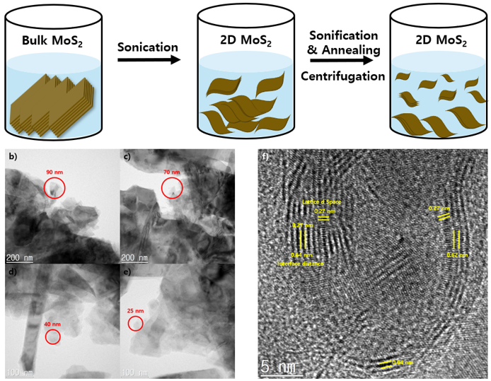
In recent semiconductor scaling, encountering physical limits, 2D materials are gaining significant attention. Among them, TMDs and MXenes are actively researched as 2D materials due to their superior electrical conductivity and physical stability compared to graphene. Among TMDs, MoS2 is bound by Van der Waals forces, allowing easy separation into individual sheets using sonification, and it has the advantage of being able to adjust the Bandgap according to the number of 2D layers. Furthermore, as MoS2 approaches 2D, it becomes mechanically flexible and exhibits a Direct Bandgap, with the advantage of a wider photoactive region compared to Si or GaAs. This study developed a radiation detector with an organic/inorganic hybrid active layer using MoS2 nanocrystals of various sizes obtained through ultrasonic exfoliation and centrifugal separation processes, as illustrated in Fig 1a. TEM images of MoS2 nanocrystals obtained at each rpm in Fig. 1b~e show that as the centrifugation speed increases, the size decreases. The TEM image of MoS2 nanocrystals obtained at 8000 rpm in Fig 1f confirms that even as the size decreases, the 2D characteristics of MoS2 nanocrystals are maintained.
The organic material used in the experiment is P3HT:PCBM, and to assess the effect of MoS2 size variations, the mixing ratio of MoS2 was fixed at 3 wt% for the experiments. Figure 2 shows the corresponding energy levels of the proposed detector and the process of charge collection.
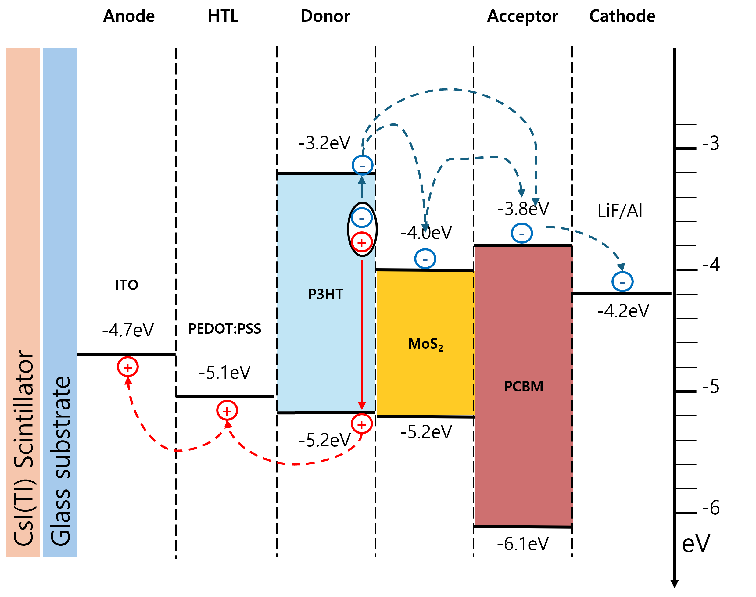
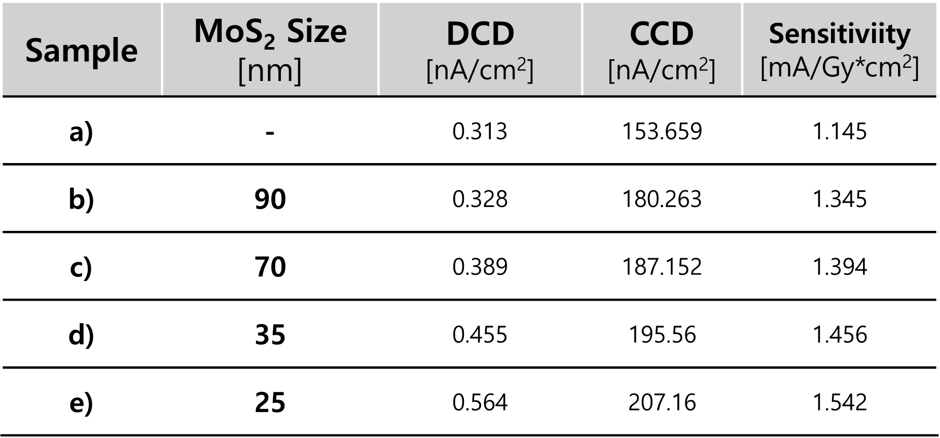
Fig 3 shows the parameters of the radiation detectors for samples according to the size of MoS2 used in active layer. The developed radiation detector demonstrates optimized results at 8000 rpm, showing a 34% improvement in sensitivity compared to detectors without MoS2 in the active layer.
Our results indicate that the use of 2D MoS2 nanocrystals is a promising approach to enhance the properties of semiconductor materials, suggesting its applications in a wide range of fields including electronics and optoelectronics engineeringemiconductor materials, suggesting its applications in a wide range of fields including electronics and optoelectronics engineering.
Low-dose computed tomography (CT) imaging is a crucial diagnostic tool that reduces radiation exposure for patients but often suffers from increased noise and reduced image quality. To address these challenges, we developed a hybrid network that combines the strengths of stochastic block (StoBlock) and residual dense networks (RDN) to enhance the denoising of low-dose CT images. The hybrid network employs a StoBlock with distribution stochastic window to capture both local and global features of images, effectively reducing noise while preserving important details. The transformer processes features across the entire image, enhancing the extraction of relevant features and suppressing unwanted noise. Complementarily, the RDN component refines image details through densely connected convolutional layers. These layers learn and integrate residual features across the network, improving the overall image quality by enhancing texture and edge preservation. We trained this network using a mean absolute error (MAE) loss function, chosen for its stability in training and sensitivity to outliers, crucial for high-quality denoising. The performance of our hybrid model was compared against several advanced denoising methods using metrics like peak signal-to-noise ratio (PSNR), structural similarity index (SSIM), and root mean squared error (RMSE). Our results demonstrated superior performance of the hybrid network, with higher PSNR and SSIM scores indicating not only reduced noise but also improved visual quality. These outcomes suggest that our hybrid network can significantly enhance diagnostic accuracy while maintaining low radiation exposure, promising better patient outcomes and safer diagnostic practices.
The Tile Calorimeter (TileCal) is the central hadronic calorimeter of the ATLAS detector at the Large Hadron Collider (LHC) at CERN. It plays an important role in the reconstruction of jets, hadronically decaying tau leptons and missing transverse energy, and also provides information to the dedicated calorimeter trigger. This sampling calorimeter is composed by the plastic scintillating tiles and steel absorbers. The scintillating light from the tiles defining around 5000 cells is read-out by the wavelength shifting fibres coupled to 9852 photomultiplier tubes (PMTs).
The dedicated calibration systems are used to monitor and calibrate each stage of the signal production from scintillation light to the signal reconstruction. A Cesium radioactive source assesses the response of the whole detector, a laser system provides controlled light pulses to monitor the PMTs and the front-end electronics is calibrated through charge injection. Besides, the integrated cells’s signals from minimum bias events provide auxiliary information on the response stability from the whole detector during proton-proton collisions.
In this presentation, the calibration and performance of TileCal using the LHC Run 3 will be presented, and the plastic scintillators’ light output loss due to integrated dose will be discussed.
Radiography is utilized in various industries and medical fields as one of the Non-destructive Testing methods, enabling the acquisition of intrinsic information about materials by penetrating them with radiation. Particularly, by employing methods such as dual-energy X-ray radiography or X-ray combined neutron radiography, it is possible to discern different materials based on the differences in their attenuation coefficient ratios. In this study, a dual particle radiography system was developed using the organic plastic scintillator EJ276G and the SiPM model Hamamatsu S13360-6025CS. Material phantoms including PVC, Aluminium, Acrylic, Lead, Copper, Brass, Teflon, and Stainless steel were utilized, with a Cf-252 source (76.2 μCi) for fast neutron imaging and a Cs-137 source (75.5 μCi) for gamma-ray imaging. After obtaining the neutron and gamma-ray intensities for the eight substances mentioned above, the intensities in air were log-transformed to calculate Σt and μt values for each substance. Afterward, the attenuation coefficient ratio between fast neutrons and gamma rays was defined to obtain the R-value for each material. The effective atomic number (Zeff) ranged from 6.47 (acrylic) to 82 (lead) with R values ranging from 0.37 to 5.23. Through this, the feasibility of classifying various materials from a homeland security perspective was confirmed. Future studies will collect time of flight (TOF) data from radiography systems to determine detector response functions. Subsequently, we will use Monte Carlo simulations to tabulate the R-values of various effective atomic numbers.
In 2021, the ATLAS collaboration started the production phase of the new Inner-Tracker (ITk) strip sensors, so-called ATLAS18, that should be able to withstand the extreme radiation conditions expected for the forthcoming High-Luminosity Large Hadron Collider (HL-LHC) upgrade. The new all-silicon ITk detector will reach unprecedented accumulated fluences and ionizing doses, caused by the increase of the total integrated luminosity. Previous studies with prototypes showed that these severe radiation conditions can modify some of the electrical characteristics of the strip sensors in working conditions.
The objective of the study is to evaluate the evolution of the performance of the new ITk strip sensors as a function of radiation exposure, to ensure the proper operation of the upgraded detector during the lifetime of the experiment. For this purpose, ATLAS18 Barrel Short-Strip sensors with final layout design have been irradiated with neutrons at the TRIGA reactor in Ljubljana (Slovenia), and with gammas at UJP Praha (Czech Republic). The irradiations cover a wide range of fluences and doses that ITk will experience, going from 1e13 neq·cm-2 and 0.49 Mrad, to 1.6e15 neq·cm-2 and 80 Mrad. The split irradiation enables a proper combination of fluence and dose values of the HL-LHC condition which is not possible with a proton irradiation in 10 to 100 MeV kinetic range. The irradiation exposures used are equivalent to operational intervals between the first few days and the end of the HL-LHC data collection, including a 1.5 safety factor.
A complete electrical characterization of the key sensor parameters before and after irradiation is presented, including the study of the leakage current, bulk capacitance, and single-strip and inter-strip characteristics. The results confirm that the performance of the new ITk strip sensors fulfills the specifications established by the ATLAS collaboration. Additionally, the study of a wide range of fluences and doses allows to obtain detailed results about the frequency dependence of the bulk capacitance measurements, or the evolution of the Punch-Through Protection (PTP) for the radiation exposure range expected for the lifetime of the HL-LHC.
In the framework of an Italian PRIN 2022 PNRR project, we proposed to develop advanced modules for SPECT prototypes, in terms of sensitivity, spatial and energy resolution, for quantitative imaging in nuclear medicine. In this context, we developed new high-resolution cadmium–zinc–telluride (CZT) drift strip detectors for room temperature gamma-ray spectroscopic imaging. As widely demonstrated, CdZnTe (CZT) is one of the key materials for the development of room temperature X-ray and gamma ray detectors and several research groups are still involved in advances in both device and the crystal growth technologies [1,2]. The CZT detectors, equipped with orthogonal anode/cathode collecting strips, drift strips and dedicated digital pulse processing allow a detection area of 6 x 20 mm2 and excellent room temperature spectroscopic performance (0.8% FWHM at 662 keV). The capabilities in spectroscopic and Compton imaging will be presented.
[1] S. Del Sordo et al., Sensors 2009, 9, 3491–3526
[2] L. Abbene et al., J. Synchrotron Rad. 2020, 27, 319–328.
The authors acknowledge funding from the Italian Ministry for University and Research (MUR), under PRIN 2022 PNRR project No. P2022SE49Y.
With an increasing number of applications, the Timepix [1] technology is also currently studied as a possible radiation monitor [2] within the scope of Radiation to Electronics activities at CERN. During a calibration campaign at CNA 3 MV tandem facility [3], its capabilities as a beam monitor for ion beams emerged. The investigated proton and hadron beams leave multi-pixel tracks in the Timepix3 sensor, and after reconstructing the full clusters, the beam shape, size and its movement could be measured, as seen in Fig. 1.
In particular, the default instruments at the irradiation chamber that was used at CNA can only detect particle currents above 106 particles/(cm2 s). Nevertheless, the beamline has been designed including a scanning system to allow the irradiation of large areas. Although this is limited by the sample holder dimensions (16×20 cm2), depending on the beam features the full scan can be further increased. Then, by raster scanning of the beam through magnetic deflection, the current density can be dramatically decreased, to an average ion flux to the order of 102 particles/(cm2 s). The Timepix3 Radiation Monitor successfully measured such low fluxes, as well as confirming the raster scan procedure.
[1] T. Poikela et al., Timepix3: a 65k channel hybrid pixel readout chip with simultaneous ToA/ToT and sparse readout, in Journal of Instrumentation 9 (2014), pp. C05013–C05013. url: https://doi.org/10.1088/1748-0221/9/05/c05013.
[2] D. Prelipcean et al., Towards a Timepix3 Radiation Monitor for the Accelerator Mixed Radiation Field: Characterisation with Protons and Alphas from 0.6 MeV to 5.6 MeV. in Applied Sciences. 2024; 14(2):624.url: https://doi.org/10.3390/app14020624.
[3] Y. Morilla et al., Progress of CNA to become the spanish facility for combined irradiation testing in aerospace, in 2018 18th European Conference on Radiation and Its Effects on Components and Systems (RADECS), IEEE, 2018, url: htps://doi.org/10.1109/RADECS45761.2018.9328656
The High Luminosity upgrade of the CERN Large Hadron Collider (HL-LHC) requires new high-radiation tolerant silicon pixel sensors for the innermost part of the tracking detector in the CMS experiment. The innermost layer of the tracker, which is as close as 3 cm from the interaction point, will be exposed to a fluence of 2.6E16 neq/cm2 during the high-luminosity operation period. The 3D pixel sensor technology has been proven to be the best option for such a layer in terms of radiation tolerance and low power consumption. An extensive program aiming at 3D pixel sensors has been carried out in the context of the CMS tracker R&D activities. The sensors have been produced by the FBK (Trento, Italy) and CNM (Barcelona, Spain) foundries. They are interconnected with the CROCv1 readout chip, which is a prototype of the final version that will be mounted in the upgraded tracking detector. The modules have been tested on beam at CERN and DESY, before and after irradiation up to an equivalent fluence of about 1.6E16 neq/cm2. An overview of the results obtained in the latest beam test experiments will be presented, including hit detection efficiency and spatial resolution. The analysis of collected data shows excellent performance, with around 98% hit detection efficiencies measured after irradiation.
Background and Aims: Accurate energy measurements imparted by single particles under high-flux conditions are essential for various applications including radiotherapy, space applications, and accelerator physics. Challenges emerge when: i) particle count rate on the detector exceeds 10^5 particles/s and particle overlapping occurs, ii) short-pulsed beams necessitate high temporal resolution, iii) highly ionizing particles induce quenching effects/energy saturation in detection systems.
Materials and Methods: For this work, a novel ASIC-based MiniPIX-Timepix2 pixel detector with a silicon sensor was used to address the aforementioned challenges. The detector's ability to resolve challenges related to high-linear energy transfer (LET) particles including ions, with therapeutic fluxes over 10^7 particles/cm^2/s and single particle deposited energies exceeding 5 MeV, is examined. The Timepix2 chip enables the detector operation for very short shutter open times down to the nanoseconds level, whereas in the Timepix3 chip the acquisition time could be decreased up to microseconds level. The experiments were carried out using carbon and proton beams with energy ranging from 97 to 400 MeV/u at MedAustron a medical synchrotron accelerator (in air), and alpha particles from a 241Am source (in vacuum and in air) with energy of 5.5 MeV.
Results: Single-particle imaging (see Figure 1) at high-flux was possible utilizing a short frame-level acquisition time of 100 ns combined with a novel detector customized configuration with adjusted per-pixel signal shaping/discharging time, see figure 1c. The energy spectra measured in clinical carbon ion flux are given in Figure 2. Furthermore, a comparison between various configurations of the detector is given together with a high-energy per-pixel calibration function, intended to correct for energy saturation effects when occur. This new calibration function for Timepix2-based detectors with standard configurations is an extension of the calibration presented by Jakubek 2011 and Sommer 2022 and it is effective above a per-pixel deposited energy threshold of ̴ 815 keV/pixel. Additionally, deposited energy spectra obtained in proton, carbon, and alpha-particle beams were compared against reference values from Monte Carlo simulations and experimental databases.
Conclusions: In conclusion, the newly developed and calibrated detection system based on Timepix2 chips provides an effective means of characterizing radiation fields through single-particle detection and identification.
References:
Jan Jakubek, Precise energy calibration of pixel detector working in time-over-threshold mode, NIMA, Volume 633, Supplement 1, 2011, Pages S262-S266, https://doi.org/10.1016/j.nima.2010.06.183.
Sommer, M., Granja, C., Kodaira, S., & Ploc, O. (2022). High-energy per-pixel calibration of Timepix pixel detector with laboratory alpha source, NIMA 1022, 165957. https://doi.org/10.1016/J.NIMA.2021.165957
SPHIRD ASIC is dedicated to high count rate single photon counting operation at the European Synchrotron Radiation Facility with Extremely Brilliant Source. The prototype IC has a matrix of 64×32 pixels with 50μm pitch. Pixel front-end electronics employs novel pile-up compensation techniques [1], while pixel logic uses relocation algorithms to increase spatial resolution [2]. This paper focuses on readout controller, responsible for matrix readout and implementing a dedicated communication protocol.
Communication with imaging sensors is asymmetric in its nature. Configuration, calibration and control data has to be sent to the sensor. These transfers are typically not time-critical or are composed of relatively short commands, hence a single, source-synchronous link is sufficient. However, in the other direction, it is desired to transfer image data as fast as possible, thus a high-speed, multigigabit serializer is a preferred option.
Having that in mind, the developed controller is divided into two parts: control path and readout path. Control path is responsible for loading configuration data to the pixel matrix and controlling chip operation. This path is bidirectional - it allows also to read image data at lower speed. Readout path on the other hand is unidirectional and designed for high data throughput. It uses an on-chip 4-lane serializer together with PCS (Physical Coding Sublayer), capable of line rates of 4Gbps per lane. Additionally, it has a configurable FSM (Finite State Machine), which allows for pixel matrix readout with different readout modes, pixel data lengths etc.
The controller has been successfully launched and tested. At the conference, we will present the main goals and requirements for the controller and the communication protocol, the partitioning of functionality between the integrated circuit and the reading system, and describe the implementation details.
PERCIVAL (Pixelated Energy Resolved CMOS Imager, Versatile And Large) [1] is a new soft-X-ray detector system also designed for modern computational synchrotron radiation microscopy. Developed collaboratively by seven research institutes (DESY, RAL/STFC, Elettra Sincrotrone Trieste, PAL, SOLEIL and Pohang Light Source), this detector is now at an advanced stage, featuring a Back-Side-Illuminated (BSI) sensor, fast acquisition/conversion electronics, and specialized control software. It represents a novel and advanced detection system that should improve existing computational microscopy techniques and potentially inspire new ones.
In December 2023, we conducted an exploratory computational microscopy experiment at the TwinMic synchrotron radiation beamline in Elettra Sincrotrone Trieste [2] (Trieste, Italy), exploiting the latest version of the PERCIVAL detector system: the updates consists of a new sensor die (with P+implant below Si02window to avoid electron trapping) and a new electronics, allowing for greater versatility and improved acquisition performances. The detector has been integrated in the existing TANGO-based beamline control system.
TwinMic operates in the 400 - 2200eV energy range and supports both Scanning Transmission Mode (STXM) and full-field imaging mode. The STXM capabilities can be extended to include phase-diverse Coherent Diffraction Imaging (CDI - Ptychography) [3], a lensless high-resolution and phase-sensitive computational microscopy technique (as in [4][5]), by using innovative algorithms [6].
In this work, we explain the (intricate) process by which we transformed RAW data from the detector into meticulously calibrated frames. Furthermore, we unveil the pioneering soft X-ray reconstructions, including absorption, differential phase contrast, integral phase, dark contrast, and phase, obtained at Elettra. These reconstructions encompass diverse subjects, ranging from test pattern objects to real samples like plant tissue and foraminifera. By leveraging the system's high-speed, the high-dynamic-range of the sensor and the new reconstruction algorithms, we achieved the highest resolution ptychography reconstructions with PERCIVAL detector to date (compared with the previous state-of-the-art [7]).
[Figure 1 in the attachment]
Fig. 1: Ptychography reconstruction of a coccolith, shown in magnitude and phase (transmission function, panel a and b), obtained from a series of far-field diffraction patterns (a representative RAW data frame in panel c). The algorithm reconstructs also the illumination (magnitude and phase in HSV color-space, panel d). The resolution of the object reconstruction is estimated with the Fourier Ring Correlation [8] (intercept with the 1/7 bit curve), showing a resolution of 40 nm (panel e). All the scale bars in panel a, b and e are 2 μm long.
BIBLIOGRAPHY
[1] Marras, A., et al. (2021). J. Synchrotron Rad. 28, 131-145. https://doi.org/10.1107/S1600577520013958
[2] Gianoncelli, A. et al.,J. Synchrotron Rad. 23, 1526, 1537. https://doi.org/10.1107/S1600577516014405
[3] D. J. Vine et al., Phys. Rev. A 80, 063823 https://link.aps.org/doi/10.1103/PhysRevA.80.063823
[4] Maiden, A. et al., Nat Commun4, 1669 (2013) https://doi.org/10.1038/ncomms2640
[5] M. W.M. Jones, et al., Opt. Express 21, 32151-32159 (2013) https://doi.org/10.1364/OE.21.032151
[6] Guzzi F, et al. PeerJ Computer Science 8:e1036 https://doi.org/10.7717/peerj-cs.1036
[7] Correa, J.et al. (2023). J. Synchrotron Rad. 30, 242-250, https://doi.org/10.1107/S1600577522010347
[8] Banterle N. et al., J. Structural Biology, Volume 183, Issue 3 (2013), https://doi.org/10.1016/j.jsb.2013.05.004
Detection and spectrometry measurements of mixed-radiation fields of high fluence and harsh radiation environments present challenges of detection selectivity and radiation damage. Silicon Carbide (SiC) as semiconductor sensor material exhibits particular advantages [1-2] of high radiation hardness, stable and high temperature operation. Available first as single pad devices, SiC pixel sensor has been newly fabricated [3] attached to Timepix3 readout chip into a position-sensitive and tracking detector used in miniaturized radiation camera MiniPIX-Timepix3 SiC [4]. The response in terms of energy-sensitive particle tracking and particle-type recognition is examined and evaluated in well-defined reference radiation fields – such as low-energy protons (8-31 MeV) [4], tunable mono-energetic fast neutrons in selected energy regions in the range 0.5 – 18 MeV produced from D-D, D-T and p-T reactions (at the Van-de-Graaff light ion accelerator, IEAP CTU Prague), energetic light ions (at MedAustron, Wiener Neustadt), energetic heavy ions (at the NSRL radiation facility, Brookhaven Nat. Lab.), protons (at the light ion cyclotron, NPI Rez) and energetic 3-22 MeV electrons (at the Microtron accelerator, NPI Rez) – see Figs 1-2. In this work we examine and describe the detection response in wide-range and resolving power of particle-type discrimination. The results, calibrations performed and developed methodology enable the use of SiC as a particle tracking and imaging detector for application in complex and harsh radiation fields produced at particle accelerators, nuclear reactors, radiotherapy facilities, radionuclide-source environments including neutrons.
References
[1] M. De Napoli, et al., Front. Phys. 10 (2022) 898833
[2] F. H. Ruddy, et al., IEEE NSS 69 (2022) 792-803
[3] B. Zatko, et al., JINST 17 (2022), C12005
[4] A. Novak et al JINST 18 (2023) C11004
Acknowledgments
Work at Advacam was performed in frame of ESA Contract DPE 4000130480/20/NL/GLC/hh. The teams of IEAP CTU and STUBA at the experiments at the IEAP CTU were supported by Project Danube Strategy 2022 No. DS-FR-22-0012.
The High Pressure Neutron Diffractometer (HPND) is designed to explore new phases and physical properties of materials under high pressure at the China Spallation Neutron Source (CSNS). A large-area 3He tube array detector has been adopted as position sensitive neutron detector. The 3He tube array contains 116 detection unit, each unit consist of eight 3He tubes. A dedicated readout electronics system is developed to acquire the neutron hit events, calculate the position and flight time information of the scattered neutrons. For each 8-3He-tube detection unit, the readout electronics consists of two 8-channel front-end boards (FEB) and one 16-channel digital acquisition (DAQ) board. The FEB converts the charge signal into a voltage pulse signal and pre-process the analog signals; The DAQ board performs analog-to-digital conversion, event processing and data communication. Test results shows that the readout electronics system could work well, and the position resolution of the detection unit is better than 8mm.
Digital flat-panel detectors with indirect method typically uses amorphous silicon thin film transistor (TFT) or silicon CMOS (complementary metal oxide semiconductor) matrix arrays integrated with various scintillators for many X-ray imaging tasks. Conversion of X-ray energy into electric signals in flat-panel detector is implemented through a scintillating converter that emits visible lights under X-ray exposure. Because the visible light with green wavelength is emitted in scintillating film in all directions and it is changed into an electric signal in photodiode array, the light scattering and attenuation in scintillator grains play an important role for excellent spatial resolution in X-ray image quality.
In this work, high efficient scintillating films such as granular type Gd2O2S:Tb(GOS) materials with different 50-100um thickness were designed for ultra-high resolution(UHR) in digital X-ray imaging detectors. The used high resolution CMOS flat panel detectors in this experiment are consisted of silicon photodiode array with 50μm pixel pitch(theoretical resolution limit: 10lp/mm) and 20μm pixel pitch (theoretical resolution limit: 25lp/mm) respectively.
Their X-ray charaterization of high resolution CMOS imagers in combination with ultra-high resolution scintillation screens were investigated in terms of the relative light response to given X-ray exposure dose, modulation transfer function (MTF), noise power spectrum and X-ray imaging with various phantom. Through this expriment, the CMOS area imager with high resolution thin GOS films could implemented X-ray imaging task with ultra-high resolution. We predict that this new technology will show possibility for ultra-high spatial resolution in digital X-ray imaging tasks such as medical and industrial fields.
To address complexities arising from the various readout electronics for different neutron detection or imaging system, a general readout electronics platform is introduced in the paper, which can greatly reduce the difficulty of designing and maintaining readout electronics for Chinese Spallation Neutron Source (CSNS). The fundament thought of the general readout electronic platform is achieved through the cooperation of analog and digital modules. The analog module is used to condition the input signal in order to improve the signal-to-noise ratio. The digital module is a system-on-chip (SoC) solution, which can facilitates the following functionalities: analog-to-digital conversion, digital signal processing, communication and providing embedded Linux system for software development. The introduction of SoC architecture make the general readout electronics platform become a more modern system, which can flexibly achieve the data analysis, physical information extraction and access to data stream-processing platform, such as Apache-Kafka. As well as provide a brand new perspective on the process of developing next-generation neutron spectrometers software and hardware readout system.
Fast neutron radiography is a promising non-destructive testing method that can be utilized in various industries. It provides different information compared to conventional radiography based on X-ray, gamma-ray, and thermal neutron, due to differences in attenuation with materials. There are two main methods for measuring fast neutrons: a thermal neutron capture detection system and a recoil proton-based neutron scattering detection system, with the latter being particularly suitable for fast neutron radiography. Among various recoil proton-based neutron scattering detectors, organic plastic scintillators are highly valued for their long-term stability, excellent hardness, and availability in various sizes. However, despite these advantages, organic plastic scintillator has poor pulse shape discrimination (PSD) performance which cannot differentiate fast neutron from background gamma-ray for the whole energy range in PSD. Given the vast amount of data generated in fast neutron radiography, automatic classification system is needed for efficiently processing large datasets, enabling accurate and quick identification of fast neutrons. In this study, we developed an automatic classification algorithm using machine learning that automatically classifies fast neutrons from gamma-ray for whole energy range in PSD result. The proposed automatic classification algorithm consists of two steps. First, data in the high energy region are clustered by Gaussian Mixture model, which is an unsupervised machine learning algorithm. Then, data in the low energy region is classified based on the clustered results by Gaussian Naïve Bayes model which is a supervised machine learning algorithm. Evaluation was conducted by applying the automatic classification algorithm to the neutron and gamma-ray signals obtained by the time of flight (TOF) measurement. The AUC of the ROC curve was 0.9390, which showed excellent classification performance.
The organic-inorganic hybrid perovskite have various advantages, such as outstanding electronic properties, tunable bandgap, wide-range optical absorption, high ambipolar carrier transport properties, long carrier diffusion length, trivial exciton binding energy, and low-temperature processability and flexibility. However, a major challenge associated with organic-inorganic hybrid perovskite is their sensitivity to moisture and heat, mainly due to the presence of volatile organic compounds. There are various strategies to overcome moisture problem such as interface treatment, additive, antisolvent, dopant, etc. Among them, we demonstrate an interface engineering by blending non-fullerene polymers to transport layer.
In this paper, an organic-inorganic hybrid perovskite photodetector with binary-ETL was investigated as a candidate for the indirect-type X-ray detector. The active layer composed with MAPbI3 and the non-fullerene Y6 as the first acceptor (A1) and PC71BM as the second acceptor (A2). The incorporation of PC71BM:Y6 at the heterojunction interface facilitates electron extraction, leading to efficient separation and transport of photoexcited electron-hole pairs. Furthermore, The hydrogen bonds between MAPbI3 and Y6 passivate the defect on the surface of the perovskite, reducing the roughness and thickness of the ETL while maintaining good film morphology. Moreover, optimizing the spin coating process for PC71BM:Y6 binary-ETL results in enhanced crystalline and structural homogeneity, characterized by larger grain size and higher coverage. Consequently, this optimization enhances electron extraction ability and suppresses charge recombination loss, significantly enhancing the performance of the PC71BM:Y6 binary photodetector . Figure 1. shows a energy band diagram of the proposed indirect X-ray detector with PC71BM:Y6 ETL. Experiments to extract the current density-voltage (J-V) characteritics were performed by different blending ratios of PC71BM:Y6(100:0, 75:25, 50:50, 25:75). As depicted in Figure 2, to collect the charge generated during X-ray exposure, a −0.6 V bias was applied between the cathode and anode of the detector and it was irradiated for 1.57s. The radiation parameters during X-ray exposure, such as collected charge density (CCD) and sensitivity of the detector coupled with the CsI(TI) scintillator, were calculated based on the number of collected charges and absorbed dose.Up to now, the highest CCD of 20.87 μA/cm2 and sensitivity of 6.24 mA/Gy∙cm2 were obtained at the condition of PC71BM:Y6 = 75:25 in Figure 3. The CCD and sensitivity tend to increase as the content of Y6 in the acceptor increases, and tend to decrease above 50:50 content.
Our results suggest that the use of binary-ETL represents a promising approach for enhancing the properties of the detector and have important applications in a wide range of fields, including electronics, optoelectronics. The synergy at the material interface not only optimizes the electronic characteristics of detector but also mitigates inherent vulnerabilities such as sensitivity to environmental factors.
In the realm of low-energy nuclear physics experiments, Active Target Time Projection Chambers (AT-TPC) proves advantageous for studying nuclear reaction kinematics. Specifically, it allows investigation into phenomena like the alpha cluster decay of $^{12}C$ by precisely tracking the reaction products produced within the active gas medium of the TPC. The tracking capability of the TPC critically depends on the homogeneity of the electric field applied across its drift medium. However, this homogeneity is significantly influenced by the space charge generated by low-energy projectiles and reaction products within the active gas medium through the ionization process. In our research, we developed a mathematical model based on a hydrodynamic approach to simulate the space charge effect caused by the alpha beam on the TPC’s performance. We achieved this using a commercial Finite Element Method (FEM) package available in COMSOL Multiphysics. The primary ionization resulting from alpha particles was simulated using Geant4, while the electron transport parameters for the active gas were obtained from MAGBOLTZ. Our findings include the impact of space charge on the applied electric field of the TPC and the angular and spatial resolution of scattered tracks. These results were obtained for beam currents ranging from 2.5 pA to 25 pA. Additionally, we employed the same model to simulate the temporal evolution of scattered tracks for $^4He$ and $^{12}C$ in active gas mediums, specifically $Ar+CO_2$ with volumetric ratios of 90:10. We also explored various readout geometries for the TPC to determine the optimal pad dimensions and the number of pixels at the TPC end cap necessary for resolving scattered particle tracks accurately. Furthermore, we developed a tracking algorithm capable of distinguishing between multiple tracks associated with scattered events and the $^{12}C$ breakup. Based on our simulation results, we are currently in the process of designing a 64-channel Micromegas-based prototype TPC.
Monte Carlo particle transport codes are usually used to simulate the processes energies beyond the SEM range of few tens of KeV. The functionality of some of these codes is however broader and they can be successfully used to simulate the physics in the range corresponding to SEM. This contribution demonstrates the usage of two closely related codes for the simulation of the SEM detector systems.
Geant4 is the toolkit written in C++ which simulates the passage of the particles through the matter and is mainly used in high energy, nuclear and accelerator physics. It incorporates several models for the interactions of the electrons/photons with matter and proved to provide very good predictions of BSE yields (Figure 1), response functions for semiconductor detectors or optical photon transport from scintillators to PMT. Geant4 was also used for several smaller tasks like the simulation of electron/X-ray passage through thin layers (eg. CNT membranes), the spectra of the transmitted particles, etc. As such, the toolkit provides an important step between the analytical calculations and costly experimental validation.
Allpix2 extends the Geant4 ability with the simulation of the transport of electron-hole pairs in the semiconductor materials. The tracked particles (X-rays, electrons) are transported using the Geant4 code in the detector geometry (detector housing, dead layers, etc.). The energy deposited in the sensitive part of the semiconductor detector is converted to electron-hole pairs, Allpix2 code takes over their transport in the user defined electrical/magnetic fields using a rich set of models describing charge carrier mobility, recombination, trapping, etc.
Both codes have greatly deepened our understanding of the complex processes within detectors, paving the way for leveraging this knowledge in the creation of a new simulation framework designed specifically for detector systems.
We focus on particle detectors for electron microscopy and especially on the image quality improvement with very high sensitivity and low-noise electron imaging. Solid-state detectors offer the advantages of direct detection, response linearity, thin and customizable geometry including arbitrary segmentation. This, in combination with signal electron filtering in the SEM objective, promises the required flexibility in contrast formation. The present work aims to achieve the ultimate performance of this type of detector, which is significantly limited by the large parasitic capacitances in today's designs, by placing the bare active silicon op-amp chip on the sensor substrate.
We present the design and measured performance of an ASIC-like transimpedance amplifier based on bare-die op-amps placed directly on the sensor substrate. This leads to a reduction in input capacitance, fine controlling of stray parameters and ultra-low-noise performance. It is a cost-effective solution tailored for pixel imaging, strip or segmented detectors with a few pF input capacitance. A hybrid integrated circuit PoP with a two TIA channels was designed and wire-bonded to the detector segment. We have successfully used this approach to construct a high-sensitivity, high-bandwidth BSE detector capable of 25 ns dwell time, which is an order of magnitude better than currently used solutions. We are investigating the effects of PCB leakage, excess noise from resistors, parasitic capacitance that limits bandwidth, local overheating of electronics in vacuum, and ways of using ceramic substrates instead of conventional laminate substrates. The result is a new and more sophisticated front-end circuit to extract the signals, as in the case of hybrid pixel technology.
The Large Hadron Collider (LHC) will soon be upgraded to prepare for the high-luminosity phase. To cope with the increase in background rates and trigger requirements, the CMS muon system is being upgraded by installing additional sets of muon detectors based on Gas Electron Multiplier (GEM) technology. The GE2/1 station will consist of 72 GEM chambers, comprising 288 modules, covering the pseudorapidity range between 1.62 and 2.43. The GE2/1 chambers are being produced at this moment and the first chambers were installed at the beginning of this year.
This talk will focus on the quality control of these first GE2/1 chambers, with a dedicated focus on the results obtained with the cosmic test stand. Also the performance of the first two production chambers installed in the CMS experiment will be discussed.
The inner detector of the present ATLAS experiment has been designed and developed to function in the environment of the present Large Hadron Collider (LHC). At the ATLAS Phase-II Upgrade, the particle densities and radiation levels will exceed current levels by a factor of ten. The instantaneous luminosity is expected to reach unprecedented values, resulting in up to 200 proton-proton interactions in a typical bunch crossing. The new detectors must be faster and they need to be more highly segmented. The sensors used also need to be far more resistant to radiation, and they require much greater power delivery to the front-end systems. At the same time, they cannot introduce excess material which could undermine tracking performance. For those reasons, the inner tracker of the ATLAS detector was redesigned and will be rebuilt completely.
The ATLAS Upgrade Inner Tracker (ITk) consists of several layers of silicon particle detectors. The innermost layers will be composed of silicon pixel sensors, and the outer layers will consist of silicon microstrip sensors. This contribution focuses on the strip region of the ITk. The central part of the strip tracker (barrel) will be composed of rectangular short (~ 2.5 cm) and long (~5 cm) strip sensors. The forward regions of the strip tracker (end-caps) consist of six disks per side, with trapezoidal shaped sensors of various lengths and strip pitches. After the completion of final design reviews in key areas, such as Sensors, Modules, Front-End electronics, and ASICs, a large scale prototyping program has been completed in all areas successfully. We present an overview of the Strip System and highlight the final design choices of sensors, module designs and ASICs. We will summarise results achieved during prototyping and the current status of pre-production and production on various detector components, with an emphasis on QA and QC procedures.
The X-ray imaging systems dedicated for X-ray spectroscopy, based on a semiconductor strip sensors have been recently an important research topic. The most important research objective is working towards improvement of the spectroscopic and position resolution features [1-3]. In spectroscopic applications the short strip silicon detectors are widely used due to their relatively small capacitance and leakage current. Using strip pitch below 100 µm enables achievement of high spatial resolution.
In this work, the analysis and design of the read-out electronics for the short silicon strip detectors are presented. The Charge Sensitive Amplifier (CSA) is optimized for the detector capacitance of about 1.5 pF, and the shaping amplifier default peaking time is about 1 µs (controlled by the sets of switches). To achieve the lowest possible noise level, the sources of noise in a radiation imaging system both internal (related to the front-end electronics itself), as well as external, were considered [4]. We target the noise level below 50 el. rms, considering low power consumption (a few mW) and limited channel area. To increase the speed of incoming hits processing, the continuous-time resistive CSA feedback together with a digital feedback reset are included. The prototype integrated circuit comprises of 8 charge processing channels, biasing circuitries, reset and base-line restoration logic, and a calibration circuit.
[1] P. O’Connor and G. De Geronimo, “Prospects for charge sensitive amplifiers in scaled CMOS,” Nucl. Instruments Methods Phys. Res. Sect. A Accel. Spectrometers, Detect. Assoc. Equip., vol. 480, no. 2–3, pp. 713–725, 2002, doi: 10.1016/S0168-9002(01)01212-8.
[2] R. Ballabriga, et al.,” Photon counting detectors for X-ray imaging with emphasis on CT,” IEEE Trans. Radiation and Plasma Medical Science, vol. 5, no. 4, p. 422–440, 2021.
[3] P. Wiącek et al., “Position sensitive and energy dispersive x-ray detector based on silicon strip detector technology,” J. Instrum., vol. 10, no. 4, pp. P04002--P04002, 2015, doi: 10.1088/1748-0221/10/04/P04002.
[4] W. Zubrzycka and K. Kasiński, “Noise considerations for the STS/MUCH readout ASIC,” GSI Helmholtzzentrum für Schwerionenforschung, Darmstadt, 2018.
The authors acknowledge funding from the National Science Centre (Research Project 2020/37/N/ST7/01546).
Organic scintillators play a significant role in detecting ionizing radiation and have been widely utilized in Particle and Nuclear Physics research, as well as in their related applications, due to their cost-effectiveness. This study addresses the fundamental research and development aimed at meeting the demands of next-generation experiments in High Energy Physics, which necessitate enhancements in light yield, radiation hardness, and response speed. Traditionally, plastic scintillators incorporate organic polymeric base solvents doped with wavelength shifters (WLS) to optimize light yield. Recent investigations, however, have highlighted Polyethylene Terephthalate (PET) and Polyethylene Naphthalate (PEN) as promising alternatives, emitting blueish light when exposed to ionizing radiation. Our research focuses on the manufacturing and characterization of PET, PEN, and PET:PEN blend scintillator samples through injection molding of granular raw materials. Additionally, we explore the impact of dopants on these substrates. Comparative analysis reveals that PEN samples exhibit significantly higher light responses compared to PET samples, with specific dopants doubling PET's light yield. Furthermore, a positive correlation exists between the light response and PEN proportion in PET:PEN blended samples. This study presents preliminary evidence suggesting that suitable dopants enhance the scintillation effect of PET:PEN base mixtures, thus contributing to the advancement of organic scintillator technology in radiation detection applications.
The MAX IV Synchrotron facility in Lund, Sweden, employs more than 30 X-ray detectors and cameras that are essential for the operation of its beamlines.
Abstract The most common drivers for the choice of a certain technology are the spatial and temporal resolution, and the energy range. Different detector typologies (imaging, energy sensitive...) and technologies (photon counting, charge integrating...) respond to different experimental requirements.
Abstract The facility purchases most of the detectors from commercial partners, but some of the most cutting edge solutions are obtained instead through scientific partnerships with other laboratories. In both cases we take care of the characterization and calibration of all detectors as well as the integration with the rest of the beamline and the IT infrastructure of the laboratory.
Abstract We will present an overview of the technologies employed, of the operational aspects and support systems for these detectors.
The combination of scintigraphy and fluoroscopic X-ray imaging enables shorter and easier interventional procedures involving radionuclides, such as radio embolization. As a result of the simultaneous acquisition of anatomical and nuclear information, this could reduce the burden for the patient and simplify hospital logistics. While various multimodal imaging techniques are already available and in use \cite{cherry2009multimodality}, this new approach mounts a gamma camera directly behind a flat-panel X-ray detector on a clinical C-arm \cite{van2019dual}. Advantages of this hybrid C-arm for interventional x-ray and scintigraphy imaging (IXSI) include a compact design and a naturally good image alignment. However, several shortcomings still need to be addressed, especially the X-ray induced blinding effects in the gamma camera \cite{koppert2018impact}. To this day, most clinical gamma cameras use NaI(Tl) as the scintillator. This material has a relatively high afterglow, which gives rise to a background signal following each X-ray pulse. This high background obscures the signal generated by the gamma photons, which are emitted by the radionuclide \cite{koppert2019comparative}. Thus, this research focuses on finding a scintillator with similar attributes as NaI(Tl) but with lower afterglow.
To find such, a series of GATE simulations of the IXSI hybrid C-arm detector were performed, in which the energy deposition in the gamma camera due to a typical X-ray-scan was calculated for twelve different scintillation materials. From the X-ray energy deposition within each type of crystal, the scintillation light emission and afterglow could be estimated. The afterglow intensity was subsequently compared to the light signal generated by a single $140\,\mathrm{keV}$ photon in the same scintillation material, by calculating the ratio of the light yields due to the $140\,\mathrm{keV}$ photon and the afterglow at $100\,\mathrm{ms}$ after the X-ray pulse. The five scintillators with the highest signal-to-background ratios were chosen for further in-house testing. These were CeBr3, CdWO4, NaI(Tl, Y, Sr), NaI(Tl, Sr) and CsI(Tl, Sb, Bi). From these, NaI(Tl, Y, Sr), NaI(Tl, Sr) and CsI(Tl, Sb, Bi) are newly developed materials. The in-house measurements will at least consist of afterglow-, decay-time- and energy-resolution-measurements.
Extensive results from the simulation and results from the in-house measurements will be presented at the conference.
\begin{figure}[ht]
\begin{minipage}[c]{0.4\linewidth}
\includegraphics[width=\linewidth]{Screenshot from 2024-03-18 16-10-21.png}
\caption{Simulated 'IXSI' hybrid C-arm detector prototype in Gate9.2.}
\end{minipage}
\hfill
\begin{minipage}[c]{0.4\linewidth}
\includegraphics[width=\linewidth]{Edep-Analyse.png}
\caption{Afterglow from an X-ray pulse for various scintillators (solid lines) and the corresponding light yields for one incident $140\,\mathrm{keV}$ photon (dashed horizontal lines).}
\end{minipage}%
\end{figure}
Coded Aperture γ-cameras, which have been utilized for over three decades in diverse fields such as astrophysics, nuclear facility decommissioning, and nuclear medicine, play a crucial role in imaging radioactive source distributions. These devices capture the spatial coordinates of γ-emitters within their field of view by leveraging the pattern of a coded-aperture mask. This mask projects a shadowgram onto pixelated detectors, which is essentially the coded aperture projection created by the differential gamma photon counts filtered through the mask's opaque and transparent regions.
Traditionally, the processing of shadowgrams involves correlating them with a digital matrix that mimics the mask pattern. The correlation matrix generated from this process highlights a peak value that accurately indicates the direction from which the radioactive source originates.
In this work we introduce the use of convolutional neural networks (CNNs) for the analysis of these images under near-field irradiation conditions, making it particularly suitable for medical applications.
With this approach we are able not only to identify the direction but also to estimate the three-dimensional position of the source in spherical coordinates. This includes the computation of the θ (theta) and φ (phi) angles, along with the magnitude of the R vector. This 3D localization capability enhances the accuracy and utility of γ-cameras, especially in environments where precise spatial resolution is critical, such as in targeted radiation therapies and diagnostic procedures in nuclear medicine. This methodology significantly refines the potential to detect and analyze radioactive sources in a detailed and spatially complex manner.
In the experimental setup, we have been using a modified uniform redundant array (MURA) mask constructed with a very simple method, which we call it “Not Two Obscures Touching (NTOT) MURA” [1]. It is placed in front of a CdTe pixel detector with total active area 44 x 44 mm2 and pixel pitch 350 μm. The recording rate is 27 frames/sec. The energy-spectrum resolution of each pixel is 3 to 4 keV FWHM for the 141 keV photo-peak of 99mTc. The NTOT MURA mask has been placed parallel to the CdTe plane at 2 cm distance. Its basic pattern consists of 19x19 elements, the element pitch is 1958 μm and the total elements of the mask are 37x37. The distance of a point source from the detector for which an optimum Point Spread Function (PSF) is obtained is about 310 mm and it depends on the element pitch.
In this research, we have developed a deep learning model using a Convolutional Neural Network (CNN) architecture. The model features an input layer, two 2D Convolutional layers designed to extract features from recorded shadowgrams, a Max pooling layer for reducing data dimensionality, two dense layers, and an output layer. We trained the model on a dataset of 7,200 shadowgrams, which were generated through simulations using a custom, fast simulation tool [1]. This tool simulated shadowgrams based on sources placed at 7,200 random positions within the field of view (FOV), and at distances up to 100 cm from the detector plane.
To prevent overfitting, we utilized an independent set of 2,400 shadowgrams for cross-validation during the training phase. We assessed the model's performance using another separate set of 2,400 shadowgrams, with results detailed in Figures 1-3. A key feature of our approach was incorporating the magnification of mask elements into the feature space to estimate the distance between the source and the detector plane.
Figure 1 illustrates that the accuracy of estimating the source's distance is within 5%, or less for distances ranging from 300 mm to 700 mm from the detector. Beyond this distance range, the convolutional neural network (CNN) becomes less reliable in estimating the source's distance. This reduced accuracy is likely due to the inadequate magnification of the mask elements on the detector plane. This observed behavior corresponds with the correlation method used to determine the 3D spatial coordinates of radioactive sources. According to the correlation method, the optimal distance for a 19x19 MURA mask with an element pitch of 1958μm is 310mm.
Figure 2 demonstrates that the estimation of the polar angle is accurate to within 10% across the range of 15° to 45°. Furthermore, Figure 3 shows that the azimuth angle is estimated with an accuracy of less than 10% for most of its range. However, there is an increase in relative error when estimating very small azimuth angles.
Finally, the performance of the algorithm will be evaluated with data sets of experimental shadowgrams taken using cylindrical extended sources of 99mTc with a diameter of 1 cm or 2 cm. The experimental evaluation is a work in progress.
[1] Editor: Krzysztof (Kris) Iniewski, Springer 2022. Book: Advanced X-ray Detector Technologies. Chapter: Coded Aperture Technique with CdTe Pixelated Detectors for the Identification of the 3D Coordinates of Radioactive Hot-Spots. https://doi.org/10.1007/978-3-030-64279-2
[2] Ι. Κaissas, C. Papadimitropoulos, C. Potiriadis, K. Karafasoulis, D. Loukas, and C.P. Lambropoulos, 2017. Imaging of spatially extended hot spots with coded apertures for intra-operative nuclear medicine applications. Journal of Instrumentation, 12(1), art. no. C01059.
Photon-counting hybrid pixel detector chips, such as those based on the Medipix3RX technology, have been central to advancements in spectral and multi-dimensional imaging at synchrotron facilities. As these facilities continue to enhance by undergoing upgrades, there is an escalating need for large-area cameras that not only handle increased X-ray flux performances but also integrate effectively into various scientific setups with minimal power consumption.
This research focuses on optimizing the energy efficiency of Medipix3RX readout chips. We have introduced several power optimization techniques, including dynamic frequency and voltage scaling, and the incorporation of standby/sleep modes into sensor operation. These methods have significantly reduced power consumption, thereby allowing for simplified cooling systems and enhanced durability without compromising the robustness and reliability of the system.
Experimental results demonstrate that applying dynamic voltage and frequency scaling can reduce power consumption by 5%, while clock gating technique can reduce up to 23% under typical operating conditions. Furthermore, the implementation of a sleep mode in periods of inactivity has shown potential to improve sensor temperature stability while reducing overall energy requirements by up to 40% compared to traditional continuous operation. A detailed characterization of the internal parameters of the Medipix3RX analog front-end has enabled us to identify optimal operating points that balance low power consumption with high performance, crucial for maintaining low noise levels and fast count rates in challenging experimental environments.
Compton imaging is a promising gamma-ray imaging method that can visualize a radioactive source without any mechanical collimators based on the Compton scattering kinematics. Challenges of the conventional Compton imaging method are an artifact in a reconstructed image and the low signal-to-background ratio, which are caused by drawing multiple Compton cones with a calculated scattered angle. A promising approach to overcome this limitation is the measurement of recoil electron tracks in the scatterer, which can estimate the source position from on a conical surface to on an arc surface.
We have developed fine-pitch hybrid pixel silicon detectors consisting of 18 µm pixel silicon PIN sensor (HORIBA Ltd.) with 450 µm thickness and 18 µm pixel ASIC (5 mm x 5 mm) fabricated by TSMC 250 nm CMOS technology in order to measure recoil electron tracks in a scatterer. The sensor was combined with the ASIC using micro-bumps. Each pixel of the ASIC can generate digital triggers when an energy deposition in the pixel is bigger than a threshold; therefore, only pixels of an electron track can be readout. The triggers are also useful to synchronize the scatterer with an absorber of Compton cameras. We will present the detail of the detector and report on its basic performance.
During the ATLAS High-Luminosity Large Hadron Collider (HL-LHC) upgrade, the current inner detector is going to be replaced by an all-silicon Inner Tracker (ITk). The pixel detector, located in the innermost part of the ITk, comprises of 9716 modules arranged in 5 layers around the beam line. The ITk-Pixel DAQ system basic read-out chain includes the YARR software, communicating with the FELIX PCIe board acting as an interface connected through lpGBT transceivers to the on-detector front-end (FE) chips ITkPix. The FEs are grouped in triplet (3-FE) and mostly quad modules (4-FE, QM) that are installed on local supports, which are integral parts of the ITk structure. The FELIX system is also used for performing Quality Control (QC) tests during integration. The work describes the development steps and corresponding testing and read-out chain validation results. A representative read-out sub-system will be used to develop and validate the different aspects of the read-out chain. This subsystem can be a Loaded Local Support (LLS) comprising few tens of ITkPix QMs with serial powering (SP) and opto-box connection. In order to have the readout chain validated, developments on trigger and command sending and data reading of YARR FelixClient controller were consequently required to validate the read-out chain, achieved first on a lab setup with a couple of ITkPix single chip cards (SCCs) and QMs. This step has been carried out successfully, paving the road to the next LLS sub-system readout test.
X-ray imaging is an invaluable tool for noninvasive analysis in many fields ranging from basic science to medicine and security. The development of low-dose large area imaging solutions still represents an important challenge for various applications.
One solution to the imaging of large areas lies in the development of novel computational imaging systems that can overcome the limitations imposed by hardware, relying instead on numerical processing power. The single-pixel detector, depending on the application, may offer a competitive edge over conventional cameras (being a cheaper alternative to the multi-pixelated solutions). In addition, the single-pixel detector can be used to achieve improved detection efficiency, faster timing response, and good spatial resolution with low radiation dose. Moreover, this technique enables detectors to image through diffuse mediums, increasing the image quality at significant depths, solving the depth penetration issues of other imaging methods.
Another advantage of single pixel imaging is that it can be combined with compressive sensing, which significantly reduces the data storage and data transfer requirements, an important consideration for remote sensing applications or when the problem is high dimensional such as hyperspectral imaging.
In this work, we explore the application of single-pixel imaging techniques to produce two-dimensional images with high temporal resolution, using only a single detector (bulk detector). The setup, based on the application of Hadamard patterns, showed promising results, proving the ability of the system to acquire images using thin PLA based masks (up to 5 mm thickness). Both simulation, using GEANT 4, and experimental setup, based on a time projection chamber (TPC), used in this work to demonstrate this technique will be reported here along with the first results.
We present a 960 channel Integrated Circuit (IC) (see Figure 1) designed in CMOS 40nm process dedicated to biomedical imaging [1, 2], that is a continuation of our previous works [3, 4]. Each IC’s pixel is equipped with a 6-bit Analog to Digital converter (ADC) responsible for converting Charge Sensitive Amplifier’s (CSA) output pulses. The ADC conversion is started upon triggering signal provided by the Discriminator (DISCR) working with a reference energy set by the Threshold Setting block (THSET). The whole conversion and further converted data assignment to the 1 out of the 64 12-bit based counters Memory (MEM) cells is realized by the in-pixel synthesized logic. Working with the 200 MHz system clock, the single ADC conversion, its data classification, and in-pixel memory writing takes about 110 ns what taking into account pixel pitch of 75 µm results in about 1.6 Gcps/mm2. Thanks to the in-pixel memory it is feasible to collect the information regarding the incoming photons energy spectrum. The IC is under measurements, i.e. the whole chip functionality has been verified successfully and the exemplary transfer function of the 960 ADCs is shown in the Figure 2.
We are evaluating the performance of a Passive Gamma Emission Tomography (PGET) device [1] equipped with 3D position-sensitive cadmium zinc telluride (CZT) gamma-ray detectors when used for inspecting spent nuclear fuel assemblies (SFAs). Before their disposal in a geological repository, SFAs undergo verification using the PGET device, developed under the guidance of the IAEA and approved by the IAEA for safeguards inspections. Recent advancements in imaging detector technology may offer a method to extend the capabilities of such devices beyond standard safeguard applications, allowing an efficient non-invasive way to characterise the properties of nuclear fuel assemblies accurately.
The efficiency of the currently used small CZT detectors is restricted by the limited likelihood of full gamma-ray absorption, which is needed for optimal imaging information. Employing larger CZT detectors would increase the probability of capturing the full energy of gamma rays, thereby enhancing the sensitivity of the PGET device and the quality of the reconstructed images. Large CZT detectors need to be position sensitive to determine through which collimator slit a gamma ray travelled. Position sensitivity results from the pixelated readout of the CZT crystals. Pixelation potentially increases the spatial resolution of the system, which is currently determined by the collimator used. Pixelation allows resolving the position of arrival up to (readout pitch)/$\sqrt{12}$. We are additionally exploring the potential of utilising Compton imaging to provide information on the origin of gamma rays along the SFA.
Simulations are used to estimate the increase in full photon absorption efficiency when comparing large and current, small, crystals. A dedicated simulation is created using Geant4, where gamma rays of energy 661.7 keV are targeted to the model describing the approved apparatus now equipped with 22 mm x 22 mm x 15 mm crystals of CZT. It is observed that the efficiency for photon absorption in this case is greatly increased when compared to the existing detectors.
[1] M. Mayorov et al., "Gamma Emission Tomography for the Inspection of Spent Nuclear Fuel," 2017 IEEE Nuclear Science Symposium and Medical Imaging Conference (NSS/MIC), Atlanta, GA, USA, 2017, pp. 1-2, doi: 10.1109/NSSMIC.2017.8533017.
In recent years we have witnessed several new generations of hybrid detectors getting slow adoption in electron microscopy, mostly used as a radiation hard direct-electron camera for diffraction on TEM. We have shown previously the advantages of the use of Timepix sensor for electron backscatter diffraction (EBSD) and for the reflected Kikuchi diffraction (RKD). In combination with the high-speed electronics, we can acquire up to 2000 fps of diffraction images. In combination with online post-processing algorithms, full information about the sample crystalline lattice is obtained. After productization efforts, this technology is commercially available as an option to regular Thermo Scientific scanning electron microscope (SEM). Here we’d like to present the advantages of using a Timepix hybrid sensor for the use in 4D-STEM in SEM. The method relies on the collection of the full diffraction image of the transmitted electrons through a thin sample (10 – 150 nm) for every pixel position on the sample.
This technique offers similar performance to many TEM-based 4D STEM methods, but in 6 – 30 kV energy range and on FOVs up to mm range. The low energy implies stronger interaction in extremely thin 2D materials, allowing us to image sheet orientation, bending and stress within the sheet over very large regions of interest. Additionally, the use of such low energies mitigates knock-on damage to the 2D material lattice, which is an issue in a TEM.
With the high acquisition speed of the 4-th generation of Timepix sensor, we plan to combine the 4D-STEM with an in-situ nano-reactor. Such a combination will allow real-time in-situ experiment monitoring, revealing the chemical phase transitions spatially resolved to less than 10 nm feature sizes. Moreover, the improved resolution of the Time-of-Arrival information of the hybrid detector allows us to get sub-ns temporal insight into the chemical reaction or phase-transition on catalyst nanoparticles, nanowires or nanotubes.
Most of the commercially available MCAs for SiPM detectors provide precision spectral measurements with costly high-end components. These devices are ideal for accurate instrumentation, however the high complexity makes these devices costly and thus unavailable to wider public.
The main idea of the presented device is to develop a low-cost MCA which uses widely available of-the-shelf components while providing a spectroscopy of gamma particles with reasonable resolution. The device is based on a STM32G4 family microcontroller, which comprises precision timers with sub-nanosecond resolution, internal embedded analog amplifiers, comparators and up to 4MHz ADC. This significantly reduces required number of external components lowering price and increasing reliability.
The measurement can be configured by user and may use up to three simultaneous ToT measurements with configurable threshold levels, pulse height measurement, or combination of both. The pulse approximation based on the measured parameters can also be performed to provide peak area measurement. Results can be acquired using various connectivity possibilities such as USB, Ethernet or WiFi. Thanks to the server running on the device the measurement information can be accessed from an internet browser. With an on-board bias power supply only an external power adapter and a SiPM detector with scintillator is needed for measurement.
Spatially resolved XRD using polychromatic fan beam and a hybrid pixel detectors Timepix3
The utilization of hybrid pixelated detectors such as Timepix3 for imaging has already been proven to have many benefits compared to conventional detectors, e.g. CCDs. The proposed work exploits these benefits for material structure analysis using x-ray diffraction (XRD) with a polychromatic fan beam. This allows simultaneous analysis of material properties along the line of interest and thus provide spatially resolved information about differences in the sample structure, e.g. material impurities or uneven sample treatment.
The proposed measurement setup utilizes two Timepix3 detectors, off-the-shelf x-ray tube and a simple geometry, enabling in situ measurement.
The data provided by the Timepix3 detector contain both spatial and energy information for each detected photon and therefore advantages of a polychromatic beam can be fully exploited.
The complete data processing chain is described and the benefits of the presented approach are shown on a several measurements, performed on materials with different crystalline structures.
Photon-counting detectors (PCDs) are an emerging technology that provides energy-selective images for a single x-ray exposure. At this time when studies have begun to consider PCDs for industrial nondestructive inspection, it is significant to present a metric describing the imaging efficiency or performance of PCDs. In this study, we describe the imaging performance in terms of detective quantum efficiency (DQE) and report the results of DQE analysis for a sample PCD using a representative x-ray spectrum (70~kV and 21-mm Al filtration). The investigating PCD, a mosaic of eight small detector modules, employs two adjustable energy thresholds, and it possesses a function called an anticoincidence operation, which sums charges spread over four pixels into a pixel exhibiting the highest charge signal.
The DQE of a single-channel PCD operated with a single energy threshold, which is typically used to reject counts triggered by random pulses owing to electronic noise, is described by the conventional DQE form:
$\mathrm{DQE}_{\mathrm{sc}}(u)=\frac{\overline{c}^{2}\mathrm{MTF}^{2}(u)}{\overline{q}_{0}\mathrm{NPS}(u)},$
where $u$ (mm$^{-1}$) denotes the Fourier conjugate of the space variable $x$ (mm), and $\overline{q}_{0}$ (mm$^{-2}$), $\overline{c}$, $\mathrm{MTF}(u)$, and $\mathrm{NPS}(u)$ (mm$^{2}$), respectively, represent the average x-ray photon fluence incident on a detector, mean counts per pixel,modulation-transfer function, and noise-power spectrum. According to the recent works [1,2], the DQE formula for two energy bins, i.e. the low ($L$)- and high ($H$)-energy bins can be derived as follows:
$\begin{eqnarray*}\mathrm{DQE}_{\mathrm{mc}}(u) & = & \frac{\overline{c}_{L}^{2}\mathrm{MTF}_{L}^{2}(u)}{\overline{q}_{0}\left[\mathrm{NPS}_{L}(u)-\frac{\mathrm{NPS}_{X}^{2}(u)}{\mathrm{NPS}_{H}(u)}\right]}+\frac{\overline{c}_{H}^{2}\mathrm{MTF}_{H}^{2}(u)}{\overline{q}_{0}\left[\mathrm{NPS}_{H}(u)-\frac{\mathrm{NPS}_{X}^{2}(u)}{\mathrm{NPS}_{L}(u)}\right]}\\ & & -\frac{2\overline{c}_{L}\overline{c}_{H}\mathrm{MTF}_{L}(u)\mathrm{MTF}_{H}(u)}{\overline{q}_{0}\left[\frac{\mathrm{NPS}_{L}(u)\mathrm{NPS}_{H}}{\mathrm{NPS}_{X}(u)}-\mathrm{NPS}_{X}(u)\right]},
\end{eqnarray*}$
where $\mathrm{NPS}_{X}(u)$ represents the cross-NPS between the two energy images. If the magnitude of the cross-NPS is negligibly small, the DQE formula can be reduced to
$\mathrm{DQE}_{\mathrm{lin}}(u)\approx\frac{1}{\overline{q}_{0}}\left[\frac{\overline{c}_{L}^{2}\mathrm{MTF}_{L}^{2}(u)}{\mathrm{NPS}_{L}(u)}+\frac{\overline{c}_{H}^{2}\mathrm{MTF}_{H}^{2}(u)}{\mathrm{NPS}_{H}(u)}\right],$
giving a DQE form that is a linear sum of DQEs of low- and high-energy bin images or $I_{L}$ and $I_{H}$, respectively. The linear form of DQE of a PCD represents how efficiently the detector converts the X-ray quanta incident upon it to two energy-bin images independently.
From the measurements of DQE, we verified that, without correction for the signal and noise correlation between energy bins, the DQE could be overestimated. The anticoincidence or charge-summing operation effectively suppressed the signal and noise correlations between energy bins, enhancing the MTFs and removing the cross-NPSs. However, it increased normalized NPSs in each energy-bin image, degrading the resulting DQE performance. The figure attached in this abstract shows the DQE results obtained using $\mathrm{DQE}_{\mathrm{sc}}(u)$, $\mathrm{DQE}_{\mathrm{mc}}(u)$, and $\mathrm{DQE}_{\mathrm{lin}}(u)$ for two different PCD operations: (a) AC-off and (b) AC-on. Plot (c) compares the DQE results obtained using $\mathrm{DQE}_{\mathrm{mc}}(u)$ for AC-off and on.
A discussion is given for describing the performance gap between the measured DQE and theoretical models. The DQE forms and analysis methodologies presented in this study will be helpful for researchers who want to understand their PCD-based imaging systems.
[1] J. Tanguay, D. Richtsmeier, C. Dydula, J. A. Day, K. Iniewski, and M. Bazalova-Carter, “A detective quantum efficiency for spectroscopic x-ray imaging detectors,” Med. Phy., vol. 48, no. 11, pp. 6781–6799, 2021
[2] N. Zarif Yussefian and J. Tanguay, “An experimental framework for assessing the detective quantum efficiency of spectroscopic x-ray detectors,” Med. Phys., vol. 50, no. 3, pp. 1318–1335, 2022
This work was supported by the National Research Foundation of Korea (NRF) grant funded by the Korea government (MSIP) (No. 2021R1A2C1010161), and conducted as a part of the research projects of “Development of automatic screening and hybrid detection system for hazardous material detecting in port container” financially (20200611) supported by the Ministry of Oceans and Fisheries, Korea.
Corresponding author: hokyung@pusan.ac.kr
Gallium Arsenide (GaAs) has increasingly become a material of choice for radiation detection, effectively bridging the gap between Silicon and Cadmium Telluride-based detectors. Its rising prominence is attributed to significant advancements in crystal doping and growth techniques, which have directly influenced the detectors' performance and efficiency. To align with the trend of crystal doping via Chromium (Cr) compensation and new annealing approaches, transport properties of the material like charge transport dynamics have to be thoroughly studied.
We have investigated the dynamics of charge carriers within GaAs:Cr planar diodes under the influence of femtosecond red laser pulses. The diodes with sizes $5 \times 5 \times 0.5 \, \text{mm}^3$ were metallized with Cr on both sides with metal thicknesses of 25-50 nm. By applying different polarities of direct current (DC) biases and adjusting the intensity of laser pulses, we were able to simulate various electric field scenarios within the sensors, enabling a detailed examination of charge carrier behavior under conditions that mimic real-world applications. The experimental methodology was also extended to explore the thermal effects on charge carrier mobility, drift times, and lifetimes over a temperature range of 5 - 25$^\circ$C. Using a well-focused, collimated laser beam, we scanned the entire metallized area. This allowed us to reconstruct two-dimensional images of charge distribution, foreshadowing differences in electric field distribution under different operating modes. We found that electron mobility was in the range of 4000-4300 $\text{cm}^2/\text{V$\cdot$s}$, while hole mobility was around 750-900 $\text{cm}^2/\text{V$\cdot$s}$. From the full charge collection, the Hecht equation was utilized to effectively reconstruct the $\mu \tau$ product for both voltage polarities, providing a robust approach for understanding the interaction dynamics of the charge polarity that was drifting through the entire bulk length. With this method, we estimated that the electron mobility lifetime $\mu_e \tau_e$ for each planar detector was in the range of 1-4.5 $ \times 10^{-4}$ $\text{cm}^2/\text{V}$. Different increased photon fluxes were also studied that allowed us to find differences in the charge collection at high and low laser intensities. At lower intensities, the role of surface and bulk recombination centers became more pronounced relative to the overall carrier dynamics. We observed that the carriers were trapped or recombined before they could contribute to the total current, thereby delaying the onset of collection, and as a result, a longer signal rise time was measured.
This study enriches existing research [1]-[3] by providing additional insights into the space charge morphological distribution within GaAs:Cr sensors. Our findings highlight how the varying charge excitation and transport conditions affect space charge behavior, thereby providing information on charge transport dynamics and space charge formation.
References
[1] D. Greiffenberg, M. Andrä, R. Barten, A. Bergamaschi, M. Brückner, P. Busca, S. Chiriotti, I. Chsherbakov, R. Dinapoli, P. Fajardo, E. Fröjdh, S. Hasanaj, P. Kozlowski, C. Lopez Cuenca, A. Lozinskaya, M. Meyer, D. Mezza, A. Mozzanica, S. Redford, M. Ruat, C. Ruder, B. Schmitt, D. Thattil, G. Tinti, O. Tolbanov, A. Tyazhev, S. Vetter, A. Zarubin, J. Zhang, ``Characterization of chromium compensated GaAs sensors with the charge-integrating JUNGFRAU readout chip by means of a highly collimated pencil beam'', \textit{Sensors}, vol. 21, no. 4, 1550-1-22, 2021, doi:10.3390/s21041550.
[2] E. Belas, R. Grill, J. Pipek, P. Praus, J. Bok, A. Musiienko, P. Moravec, O. Tolbanov, A.V. Tyazhev, A. Zarubin, ``Space charge formation in chromium compensated GaAs radiation detectors'', \textit{Journal of Physics D: Applied Physics}, vol. 53, no. 47, 475102-1-8, 2020, doi: 10.1088/1361-6463/aba570.
[3] H.T. Philipp, M.W. Tate, K.S. Shanks, P. Purohit, S.M. Gruner, “Practical considerations for high-speed X-ray pixel array detectors and X-ray sensing materials”, Nuclear Instruments and Methods in Physics Research A, vol. 925, 18-23, 2019, doi: 10.1016/j.nima.2019.01.066.
For the design and operation of spacecraft in orbit it is necessary to measure and monitor the complex radiation field in outer space [1]. Also, for the assessment of radiation effects on instruments and electronic components which can be sensitive to radiation degradation and single event effects [2]. Space radiation in low-earth-orbit (LEO) contains a wide variety of particles, from energetic protons, light ions and electrons from the Earth’s radiation belts and from the Sun – in particular solar particle events and induced geomagnetic storms. Such particles exhibit a large spectrum of energy from the keV level up to tens of MeV for electrons and hundreds of MeV for protons while they interact with spacecraft in free space from all directions with high temporal, spatial and directional variability along the spacecraft orbit. Moreover, the radiation field is further modified by interactions of the primary particles in the satellite bulk material and the production of secondary radiation. Detecting and characterizing such a complex field of highly dynamic and broad distributions of varying particles and wide energy is desired in essentially all satellites ideally with a single, compact and low-power instrument. This task is achieved with the MiniPIX-Timepix3 Space radiation monitor (Fig. 1a) which has been deployed in open space onboard OneWeb’s JoeySat satellite (Fig. 1b) launched to LEO orbit in May 2023. The detector settings, operation uptime and duty factor were customized to the satellite resources and available data rate. Raw data is retrieved and processed in high resolution on ground. The Timepix3 ASIC chip provides the composition of the mixed-radiation fields (field decomposition into particle-type classes) with detailed dose rates and particle fluxes (total and partial) [3]. Deposited energy spectra and liner-energy-transfer (LET) spectra are measured in wide range with high selectivity for protons, ions and electrons – see Fig. 2. Together with the spacecraft navigation stamp, results and physics products can be also provided as detailed spatial location maps and time distributions along the satellite orbit [4].
References
[1] A. Vampola, et al., IEEE Trans. Plasma Sci. 28 (2000) 1831–1839
[2] R. Ecoffet, R., IEEE Trans. Nucl. Sci. 60 (2013) 1791–1815
[3] C. Granja, et al., IEEE Trans. Nucl. Sci. 71 (2024) 921-931
[4] C. Granja C., et al., Planetary and Space Science 125 (2016) 114-129
The Timepix3 (TPX3) detector is a hybrid semiconductor pixelated detector [1] with a radiation sensitive sensor made of semiconductor materials such as Si, SiC, CdTe or GaAs of varying thickness. The detector is being used in a wide range of applications, including medicine, high-energy physics, neutron detection and outer space. Space applications are currently expanding and, in addition to radiation monitoring in Earth orbit and on the International Space Station (ISS), applications are planned for space weather measurements in lunar orbit, on the lunar surface and on other missions. These applications include operation in challenging environments in terms of radiation flux, complex composition, and temperature range.
Silicon carbide (SiC) is a promising semiconductor material for harsh environment applications due to its high atomic displacement energy (20 - 35 eV) resulting in high radiation hardness and wide bandgap (3.27 eV at 300 K for the 4H-SiC polytype) which ensures low leakage current while also enabling wide and high temperature operation. The SiC sensor has been fabricated and tested as an imaging radiation detector with the Timepix3 ASIC chip as the first MiniPIX Timepix3 SiC radiation camera [2] with a 4H-SiC sensor. The detector provides high-resolution spectral and tracking response for high energy transfer particles [3].
For the use of Timepix detectors in harsh radiation environments, it can be challenging to maintain stable environmental conditions for measurements, such as the operating temperature of the detector. It is therefore necessary to examine the temperature dependence of these detectors under such conditions and ideally provide a correction. Therefore, the spectrometric performance of the MiniPIX Timepix3 radiation camera with a 4H-SiC sensor (80 µm epitaxial layer and 350 µm substrate) was investigated over a temperature range from 10 ℃ to 60 ℃, using energy calibration at 20 ℃. The sensor was operated with bias +200 V for an active volume thickness 65 µm. The detector was stabilized at different thermal conditions and then irradiated with characteristic X-rays and radioisotopes in the energy range from 8 to 58 keV. The results show that as the detector temperature increases, the detected energy spectrum shifts to lower values, which means that the accuracy of the measurement decreases. This effect becomes more significant as the energy of the incident radiation increases. This indicates that the distortion of the measured results does not only depend on the detector temperature, but also on the incident energy. Based on the absolute energy shift of the spectra (a few tens of eV), we found that the measurement accuracy deviation for lower energies (15.780 keV) was 2% at 10 ℃ and 12% at 50 ℃, and in the case of the higher energies (57.532 keV) the deviation was also only 2% at 10 ℃, but at a temperature of 50 ℃ it reached 19%. With regard to the analysis of the energy resolution, evaluated by the sigma value, the results indicate that the energy resolution of this detector shows a stable performance over the whole temperature range studied. In order to avoid the need to calibrate this detector for individual temperatures based on the desired applications, a compensation method has been proposed that reduces the temperature effect on the peak position.
[1] T. Poikela, et al., JINST 9 (2014), C05013
[2] B. Zatko, et al., JINST 17 (2022), C12005
[3] A. Novak et al., 2023 JINST 18 C11004
Acknowledgements: This research was carried out at Advacam (Prague, Czech Republic) under the supervision of Hab. Prof. Ing. Carlos Granja, Ph.D. as a part of an internship funded by the Erasmus+ Programme and the Doctoral Programme of FEEI SUT in Bratislava and supported by the DS-FR-22-0012 and APVV-18-0273 grants of the Slovak Research and Development Agency.
We built a lightweight gamma-ray measurement setup that can be placed in standard weather balloons and can be retrieved after the flight. This allows multiple flights with a relatively small cost. The aim is to get spectral information on radiation at high altitudes. To obtain good spectral resolution with relatively small weight we use a cadmium zinc telluride (CZT) detector which has crystal dimension of 1 cm cubed.
Standard weather balloons can reach altitudes of 40 km depending on the size and material of the balloon and the weight of the payload. Since a fully depleted CZT detector requires fields of the order of 4 kV/cm, the critical limitation at these altitudes arises from the Paschen limit. Thus, we have developed a container which can hold the detector at normal pressure at high altitudes. With commercial components we were able to keep the total weight of the system under 700 grams, way below the 2 kg limit set by aviation safety regulations. The setup consists of a power supply, a single board computer with integrated microcontroller, and the CZT detector. Based on our tests at the laboratory, the system is able to operate at temperatures down to -40 ℃ and at pressures of few hundreds of Pascals for few hours.
In this contribution we present the design of our setup and show some measurement results. The CZT detector is irradiated with laboratory sources in a temperature climate chamber that was cycled down to -40 degrees Celsius. Based on the results, we will discuss the effects of the temperature changes to the radiation measurements and spectral resolution. In addition, we will show the effects of low pressure to the electronics and the power supply. The expected response of the detector at various altitudes based on a Geant4 simulation model is also presented with the planned balloon campaigns.
Photon-counting detectors with CdTe sensors and a small pixel size suffer from a charge sharing effect which can induce multiple counts from a single interacting photon. In addition, fluorescence photons contribute to the detected signal if the energy of the incident radiation is higher than the Cd K-edge (26.7 keV). Both effects not only degrade the energy resolution, but also the spatial resolution (1). Multiple counts can be eliminated by adjusting the discriminator threshold, which should be optimised for the application.
A photon-counting CdTe detector based on the Dectris Eiger chip is now available at the Imaging and Medical beamline (IMBL) of the Australian Synchrotron and it is planned to be used in the clinical breast CT study (2). A characterisation of the Eiger detector for biomedical imaging applications with synchrotron radiation has been carried out at the ESRF (Grenoble, France) by Fardin at al. (3); In their paper, the authors always set the discriminator threshold to half the photon energy to minimise the occurrence of multiple counts of a single photon at the interface between pixels.
In the present study, flat field and slanted edge images were acquired at IMBL using monochromatic beams between 23 keV and 60 keV at different values of the discriminator threshold, corresponding to an energy range between 5 keV and 60 keV. The first set of images was used to obtain the differential counts distributions as a function of the threshold energy, while the MTFs were calculated from the second set of images (slanted edge).
The Eiger detector installed at IMBL consists of 6 horizontally aligned elements. Analysis of the differential counts shows a very consistent calibration of the threshold across the whole detector. The full-energy peak, corresponding to the incident beam energy, is always visible and data obtained using energies above the Cd and Te K-edges show additional signals due to fluorescence and escape peaks corresponding to 𝐸𝐶𝑑 = 23.1 keV and E–𝐸𝐶𝑑 , E–𝐸𝑇𝑒 respectively.
Figure 1 shows the MTF's of 23 keV and 40 keV. In each panel, the pink line is obtained from data acquired at a very low threshold (5 keV), which allows multiple counts and severely degrades the spatial resolution, the orange line is from data obtained with the threshold set to half the photon energy, the green line is the ideal MTF. The black vertical line represents the Nyquist frequency of Eiger detector.
Due to the rejection of charge-sharing induced multiple counts, the MTF obtained at 23 keV beam energy and 12 keV threshold is close to the ideal, pixel size-limited MTF. However, when the incident radiation is at 40 keV, the MTF obtained by applying the threshold at 20 keV is still far from the ideal MTF due to the presence of florescence photons.
In this poster presentation, the whole analysis across different X-ray energies and threshold, as well as the differential counts distribution, will be presented and discussed with the aim of offering guidance for optimization in various applications.
References
1) Di Trapani et al. Nuclear Inst. and Methods in Physics Research, A 955 (2020) 163220
2) IMPACT Medical Imaging: https://impact-mi.sydney.edu.au
3) Fardin et al. Physica Medica 108 (2023) 102571
Acknowledgments
C. Pwamang is supported by ICTP/IAEA STEP Program.
The Compact Pulsed Hadron Source (CPHS) at Tsinghua University is a 13 MeV/16 kW high-current proton linac-driven neutron source, serving as a platform for education and research. To leverage the facility’s capabilities, a Small Angle Neutron Scattering (SANS) instrument was among the first to be built. The primary detector of the CPHS-SANS consists of a two-dimensional array of 96 3He linear position-sensitive detectors (LPSD), each 800 mm in length and 8 mm in diameter. A modular design was implemented for ease of testing and installation, with each module comprising 16 LPSDs. To process the signals from this 2-D array detector, a compact and low-noise readout system has been developed. Recent tests of the prototype detector module with the CPHS neutron beam showed that the LPSD counting plateau was between 1450 V and 1750 V, with a slope within ±1%/100V. A conservative working voltage of 1650 V was chosen to optimize the LPSDs' lifespan. At this voltage, the position resolution achieved was 4.3 mm in the central region and 4.9 mm at the ends. Additionally, the thermal neutron detection efficiency of the LPSD was measured to be 62.2%. The testing of the remaining five detector modules will proceed accordingly, with the full 2-D array detector expected to be operational by the end of 2025.
The DSSC camera was developed for photon science applications in the 0.25-6 keV energy range at the European XFEL in Germany. The first 1-Megapixel DSSC camera, equipped with Miniaturized Silicon Drift Detector (MiniSDD), is available and is successfully used for scientific experiments at the “Spectroscopy and Coherent Scattering” (SCS) and the “Small Quantum System” instruments of the European XFEL. A second camera, based on DEPFET active pixel sensors, is in the final stages of integration. The DEPFET technology camera has significantly improved performance as it offers an order of magnitude larger dynamic range due to its unique signal compression feature at the sensor level. It also offers much lower noise (<10 el. rms) with respect to the MiniSDD version at Megaframe rate.
This work describes recent activities in the assembly, characterization, and integration of the second camera at the European XFEL facility. These steps include focal-plane modules (FPM) inspection and assembly with its electronics onto cooling blocks and into the final detector vessel, followed by Karabo, PLC, DAQ, timing and online data preview integrations and continued by rigorous in situ testing under real-working conditions using the European XFEL infrastructure. Part of the calibration and characterization are conducted in the Detector group laboratory at the European XFEL and finalized at the final instrument location.
Moreover, there is increasing interest in compact systems based on DSSC single modules at the European XFEL. Recent endeavors have led to the creation of a novel mechanics and cooling system tailored for a single module DSSC detector, planned for deployment at the SCS instrument of the European XFEL. This module, comprising 128x512 pixels, represents a fraction (1/16) of the active area covered by the 1-Megapixel camera. The new mechanics and cooling system prioritize enhancing versatility, flexibility, and installation convenience of these single modules. Such enhancements aim to streamline potential exchanges, both within and between instruments, thereby facilitating seamless instrument operations.
In the past decade, thin silicon low-gain avalanche diodes (LGADs) have attracted considerable attention due to their timing applications in High-Energy Physics (HEP) experiments [1]. Experiments such as the High-Luminosity Large Hadron Collider (HL-LHC) require timing resolution in minimum ionizing particles (mips) detection of tens of ps to reconstruct multiple tracks per bunch crossing. A conventional thin silicon sensor cannot achieve this resolution due to the low signal amplitude. The signal-to-noise ratio of the detector-readout electronics system can be increased by incorporating a layer which realize a charge gain in the detector itself (Figure 1). The gain layer constitutes a high electric field region that allows drifting carriers to ionize silicon atoms, increasing the signal amplitude. However, multiplication gain introduces an additional noise component due to the fluctuations in the number of the generated carriers [2]. The noise associated with the multiplication gain dramatically decreases the device's performance. However, no experimental studies of the Noise Power Spectral Density (NPSD) in LGADs are available in literature. In order to measure the NPSD in LGAD structures, a wideband low-noise transimpedance amplifier (TIA) has been designed (Figure 2). The design focuses on maximizing operating bandwidth and minimizing system background noise. The TIA is based on the OPA818 operational amplifier due to its high gain-bandwidth product (GBWP) (2.7 GHz), low input capacitance (2.4 pF), and low input voltage noise density (2.2 nV/√Hz). A detachable daughter board DC coupled to the TIA's input is used to test various devices. TIA is calibrated by measuring the noise of resistors at different temperatures. The measurements of TIA's input noise revealed an additional OPA's current noise component with respect to the one declared in the datasheet. The NPSD's of an LGAD is measured from 10-28 A2/Hz to 10-24 A2/Hz in the range of frequencies from 10 Hz to 3 MHz, showing a dominant white component, strongly dependent on the device bias condition and temperature. The designed transimpedance amplifier allows the accurate noise characterization of LGAD, which is a fundamental step in the analysis of the multiplication gain in LGAD structures.
[1] N. Cartiglia, et al. "4D tracking: present status and perspectives.", Nucl. Inst. Meth. Phys. Res. A, (2022).
[2] R.J. McIntyre, "Multiplication noise in uniform avalanche diodes.", IEEE Tran. on El. Dev., (1966).
Hybrid-pixel detectors bump-bonded to silicon sensors are widely adopted for X-ray detection. However, their performance deteriorates in the soft X-ray regime due to reduced quantum efficiency and signal-to-noise ratio degradation. Recent advancements in X-ray detectors for photon science applications involve hybrid detector assemblies equipped with Inverted Low Gain Avalanche Diodes (iLGADs), featuring a high electric field layer where avalanche multiplication of charges (electrons and/or holes) can take place.
Charge-integrating JUNGFRAU detectors, developed by the Paul Scherrer Institute (PSI) originally for hard X-rays, are now deployed across various synchrotron and FEL facilities. New prototypes of these detectors incorporate iLGAD sensors, expanding the scope of their application to scientific cases in the soft X-ray regime. One promising application is the Heisenberg Resonant Inelastic X-ray Scattering (hRIXS) spectrometer of the Spectroscopy and Coherent Scattering (SCS) instrument at the European XFEL, which aims to explore the limits of energy and temporal resolution for time-resolved RIXS, and for which low noise, high spatial resolution, and high frame rates are the most stringent requirements.
The pixels of the JUNGFRAU 1.0 chips contain 16 memory cells capable of storing the detected analog signal in between readout cycles, allowing for the acquisition of up to 16 images at a frame rate greater than 100 kHz (burst mode operation). Additionally, the rectangular segmentation of the iLGAD sensors consisting of 25x225 μm2 pixels allows for high spatial resolution in the energy dispersion dimension, which can be further enhanced by taking advantage of the charge sharing across pixels applying interpolation methods. This makes a JUNGFRAU detector with an iLGAD sensor an attractive option to use in the hRIXS spectrometer, allowing to resolve not only individual trains (bunches of X-ray pulses at MHz rate that arrive at 10Hz) but also individual pulses. This would bring substantial improvements over the currently implemented commercial cameras with much slower readout speed, namely allowing for train-to-train jitter correction, improving time resolution, and for alternated pumped and unpumped pulses, improving normalization.
To investigate the viability of this detector for the hRIXS spectrometer, a characterization of two iLGAD sensors was conducted at the European XFEL using PulXar, a pulsed X-ray generator featuring an electron gun of tunable energy and intensity, and a variety of selectable targets and filters. In this work we will discuss the results of this characterization, particularly focusing on noise, signal uniformity across memory cells and subpixel resolution achieved by clustering and interpolation methods. Additionally, an overview of first measurements carried out with the hRIXS spectrometer will be presented.
The detection of ionizing radiation is of eminent importance in various branches of science like in medicine, environmental monitoring, high energy physics and border security technologies, among others. The development of alternative systems for radiation detection that present versatility of applications, of easy production and manipulation with viable costs has been the focus of many recent studies in the nuclear sciences, among those the neutron detection field is one of great importance, since the main system to detect these particles is still based on helium 3, which is scarcely available, and its availability has progressively been decreased over time. Organic plastic scintillators are a viable alternative, as they are relatively easy to produce and can be manufactured in large sizes and formats. Mostly, Plastic scintillators presents several advantages over liquids or crystal, as they are more versatile than crystals, easier to produce and lower costs and much lower toxicity then the liquids. This work presents the study and development of plastic scintillators with application in the detection of fast and thermal neutrons. In this work the production of plastic scintillators with pulse shape discrimination capabilities are carried out, and finally the incorporation of different compounds containing Boron into the scintillator matrix is attempted using homogeneous and heterogeneous methods. Some preliminary results of this development are presented in this work.
Gaseous argon detectors have been widely used in dark matter searches and neutrino experiments over the last decade, due to their distinctive ionization and scintillation characteristics. The primary and secondary scintillation in argon mainly result from the radiative de-excitation of singlet and triplet excimer states produced at gas pressures above 100 mbar. This prevalent light production mechanism dominates the argon scintillation spectrum, consisting of Gaussian-like emission, centered at 128 nm, with a 10-nm width, commonly referred to as the $2^{nd}$ continuum. On the other hand, alternative scintillation mechanisms, such as neutral bremsstrahlung and $3^{rd}$ continuum emission, have been less studied due to their lower scintillation yield compared to the $2^{nd}$ continuum. Despite this, their longer wavelength region, spanning from the near vacuum ultraviolet to the near-infrared range, is typically more compatible with current photosensors, thus eliminating the need for wavelength shifters. In this study, we conducted a comprehensive investigation of the yield and time properties of the primary and secondary scintillation emissions in gaseous argon within the 160-650 nm wavelength region. Alongside the fast emission, we observed a slow component with time constants of the order of tens of microseconds. The yield and time properties of the slow contribution were studied for a wide range of electric field values.
A novel class of perovskite-like materials A3B2X9 (where A= Cs/Rb/MA, B = Sb/Bi, X= Cl/Br/I) has been highly regarded in research community as a sustainable and eco-friendly potential replacement for CdTe and CsPbBr$_3$. Our systematic investigation demonstrates that the X-ray detection performance of these Pb-free materials has been ill-characterized in the past and that the characterization measurements are vitally susceptible to environmental conditions, leading to specious high figures of merit. To decouple the photocurrent contribution by air ionization in these materials and measure their inherent detection performance, a comparative study of X-ray response was conducted in a specifically built chamber while switching its environment between air, argon-filled, and vacuum. After carefully eliminating the plausible deleterious effects of crystallographic orientation, crystal quality, and metallization interface, our findings suggest that nearly a 1000-fold higher X-ray sensitivity may be maneuvered using an argon-filled chamber with smallest metal-semiconductor contact area. The work aims to highlight the importance of air-ionization artefact to be accounted while evaluating X-ray detection response. We encourage a comprehensive X-ray detection characterization for reporting novel materials as X-ray radiation sensors.
References:
[1] Y. He, I. Hadar and M G kanatzidis, Nature Photonics 2022, 16, 14-26.
[2] X. Geng, Y.A.Chen, Y.Y. Li, J. Ren, G. H. Dun, K. Qin, Z. Lin, J. Peng, H. Tian, Y. Yang, D. Xie and T. L. Ren, Advance Science 2023, 10, 23, 2300256
Position sensitive detectors for radiation imaging have shown as very valuable technologies to further reduce the radioactive background in the very large, current and future, detectors designed to discover the signals of dark matter interaction or neutrinoless double beta decay. I will overview the activities at the Canfranc Underground Lab, with focus on recent developments in low background detectors and our current plans to develop novel screening facilities and applications.
(Single-layer) particle tracking with Timepix3 for radiation field characterization and interaction point reconstruction within MoEDAL during PbPb collisions in 2018
The MoEDAL collaboration
MoEDAL-MAPP [1,2] is an LHC experiment dedicated to search for physics beyond the standard model through detection of exotic particles, amongst others magnetic monopoles (MM) or highly electrically charged objects (HECOs). These are searched for by a background-free detection of the unique signature of a penetrating particle with large ionizing power, comparable to relativistic ions (β ~ 1) of nuclear charge Z > 5. Towards the end of 2018, 2 Timepix3 [3] detectors with 500 µm thick silicon sensors were installed [4]. These were, at that time, the only active detectors. Their aim is to provide the measurement of radiation levels (as a measure of delivered luminosity) and – by analysis of observed traces left in the single layer device – the information of particle direction, particle arrival time (with precision of <2 ns) and particle dE/dX - permanently and temporally resolved.
In the present contribution, we extend previous methodology [5] for single-layer particle tracking with Timepix3 using random forest regression to improve the stability and accuracy of the impact angle and dE/dX assignment, required in particular for relativistic particles with high energy loss in the sensor. These algorithms have been evaluated by irradiation at different angles in an ion fragments beam created by 385 GeV/c Pb beam hitting a beryllium target at the SPS (CERN). By fitting a superposition of Landau curves to the measured dE/dX spectra, fragments up to nuclear charges of Z=4 and Z=9 could be resolved for perpendicular particle impact and particle impact at grazing angle, respectively (Figure 1).
These algorithms are then applied to data taken at a distance of ~1.1 m from and with almost unobstructed view to IP8 during PbPb collisions in 2018. We will present a complex characterization of the radiation environment showing the radiation levels as a function of time, as well as the evolution of dE/dX spectra and particle directions with time during and outside of collision periods (Figure 2). We will derive methodology to determine the beam spot length from the particle directionality maps during collisions, finding the width of the interaction region to be Δ(IP)z = (12.88 ± 0.02) cm.
References:
[1] M. Fairbairn and J. L. Pinfold, Contemporary Physics, 58:1, pp. 1-24 (2017).
[2] J. Pinfold (MoEDAL collaboration), https://arxiv.org/abs/2209.03988
[3] T. Poikela et al., J. Instrum. 9 C05013 (2014).
[4] B. Bergmann (MoEDAL collaboration), PoS(ICHEP2020) 720 (2020).
[5] P. Mánek et al., J. Instrum. 17 C01062 (2022).
Acknowledgements:
B.B., D.G., P.M. and P.S. acknowledge funding from the Czech Science Foundation (GACR) under Grant No. GM23-04869M.
X-ray Virtual Histology (XVH) has been proposed as a tool for improving the workflow of histopathological evaluation. Compared to conventional histology, which is inherently a bi-dimensional technique, XVH is based on micro-computed tomography (µCT), thus providing a 3D depiction of the imaged sample. This feature proved to be beneficial in the identification of structures that exhibit a high variability across the sample thickness, such as in micro-infiltrating tumors [1]. XVH is a non-destructive technique and does not require dedicated sample preparation. For this reason, it can also be considered as an additional tool to guide the pathologist in the sample sectioning, potentially increasing the sensitivity of histological examination and reducing the burden associated with multiple sectioning.
The main challenge of XVH is related to the low X-ray contrast of soft tissue structures, which has been tackled in many cases by implementing phase-sensitive techniques. This is de-facto the imaging standard at high-coherence synchrotron radiation facilities and is becoming widely adopted also in compact tabletop systems [2].
In parallel to, but independently from, the development of XVH, the availability of small-pixel chromatic detectors has paved the way for spectral µCT applications. Specifically, adopting devices equipped with high-Z sensors, pixel-pitch below 100 µm, and charge-sharing compensation mechanisms allows material separation at spatial resolution in the order of tens of microns.
This work aims to combine XVH and spectral µCT to visualize and quantify the iodine content within pathological samples of human thyroid. The study has been conducted at the novel multi-modal X-ray laboratory PEPI [3] (INFN, Trieste), employing a CdTe spectral detector [4] (Pixirad-PixieIII) featuring a pixel pitch of 62 µm, a 512×402 pixel matrix, two thresholds per pixel and the charge sharing compensation, and a tungsten anode microfocal X-ray tube, with an adjustable source size in the range 5 to 30 µm. To implement propagation-based phase contrast, the detector was positioned ~40 cm downstream from the sample, and the magnification was adjusted to have an effective pixel size between 15 and 20 µm (depending on the sample size). Two consecutive scans with different lateral displacements of the detector were performed to extend the field of view, yielding axial slices with lateral dimensions in the order of 1400 pixels. Accurate material decomposition was ensured by a thorough modeling of the detector’s spectral response which was obtained from a dedicated Geant4 simulation incorporating the experimental characterization of the device [5].
The imaging results were benchmarked against scans of the same samples performed at the European Synchrotron Radiation Facility (ESRF, beamline BM05) in the propagation-based mode, at a pixel size of 6.5 µm, and monochromatic radiation at two energies below and above the iodine K-edge (33.2 keV).
Results demonstrate a good correspondence in the iodine distribution within the sample between synchrotron and laboratory-based images (see attached figure a), which exhibit sensitivity to concentrations down to ~1 mg/ml. Concerning soft tissue visibility, the laboratory spectral µCT can capture the main features (parenchyma, lesion, capsule), despite the overall image quality being inferior to the synchrotron scan.
When comparing different samples, each with a different pathology, a major variability in the iodine maps is observed, corresponding to different distributions and health status of the thyroid's follicular component, the primary iodine reservoir. Additionally, large differences in the total (0.02 – 0.20 mg) and mean (0.1 – 1.1 mg/ml) iodine contents, readily computed from iodine maps, were observed. Although these findings need to be confirmed on a larger number of samples, the presented results suggest that spectral XVH can be used for providing quantitative insight into thyroid specimens, potentially aiding pathological evaluation and therapeutic management.
References
[1] S Donato et al., EPJ Plus (2024), in press
[2] K Tajbakhsh et al., IEEE TMI (2024). 10.1109/TMI.2024.3372602
[3] L Brombal et al., Scientific Reports 13.1 (2023), 4206
[4] R Bellazzini et al., JINST 10.01 (2015), C01032.
[5] V Di Trapani et al., Optics Express 30.24 (2022), 42995-43011.
We acknowledge financial support under the National Recovery and Resilience Plan (NRRP), Mission 4, Component 2, Investment 1.1, Call for tender No. 1409 published on 14.9.2022 by the Italian Ministry of University and Research (MUR), funded by the European Union – NextGenerationEU– Project Title A compact multimodal X-ray system for 3D micro-imaging of soft tissue based on the integration of spectral and phase-contrast techniques – CUP J53D23014070001 - Grant Assignment Decree No. 1383 adopted on 01/09/2023 by the Italian Ministry of Ministry of University and Research (MUR) and from INFN-CSN5, call 22260/2020, project PEPI
In this work, a method for enhanced detection and imaging of the radiation field generated in pencil beam scanning (PBS) proton therapy delivered at conventional and ultra-high-dose rates (UHDR) is presented. This work specifically aims to quantify the dose, flux and linear energy-transfer spectra (LET) of the stray radiation measured outside the target volume including contribution from thermal neutrons.
A semiconductor pixel detector Timepix3 with silicon sensor in miniaturized electronics [1] was used to image particles including thermal neutron fields produced in a water phantom. The experiments were carried out at the Proton Therapy Center Czech (PTC), Prague, Czech Republic, using clinical proton beams and at the University Proton Therapy Dresden, Germany, using UHDR proton beams both produced by IBA isochronous cyclotrons. The detector equipped with a neutron converter attached to a part of the sensor (Fig. 1b) was prior calibrated at reference radiation fields at the Czech Metrology Institute, Prague, Czech Republic [2], including the thermal neutrons. Interactions of various types of particles were recognized and discriminated using pattern recognition and artificial intelligence algorithms and compared to Monte Carlo (MC) simulations. The 2D visualization of the integrated mixed radiation field outside the target volume in the region marked on Figure 1e at a depth of 15 cm in water is displayed in Figure 2. An example of particle discrimination of thermal neutron interactions from mixed field is shown in Figure 2c. The flux of stray particles including protons, heavier ions, thermal neutrons, photons and electrons was measured and compared to MC simulations. Furthermore, the flux of thermal neutrons from Figure 3 is converted into equivalent dose [2]. Results of dose rate measurements in conventional and UHDR proton beams were provided for individual classes of particles. The thermal neutron field in the mixed-radiation stray fields of PBS proton therapy can be measured with high discrimination by the Timepix3 detector. Such detailed spatial mapping of thermal neutrons has an application in, for example, out-of-field dosimetry and research in Neutron Capture Enhanced Particle Therapy [3]. Besides thermal neutrons and protons a large flux of electrons and gamma rays was also measured. Moreover, in the plateau region of the Bragg curve, secondary ions were identified. These findings underscore the importance of comprehensive radiation characterization for optimizing therapeutic outcomes and ensuring patient safety.
Reference:
[1] Oancea, et al. (2023) Out-of-field measurements and simulations of a proton pencil beam in a wide range of dose rates using a Timepix3 detector: Dose rate, flux and LET. Physica Medica, 106, 102529. https://doi.org/10.1016/J.EJMP.2023.102529
[2] Oancea, et al. (2023a). Thermal neutron detection and track recognition method in reference and out-of-field radiotherapy FLASH electron fields using Timepix3 detectors. Physics in Medicine & Biology, 68(18), 185017. https://doi.org/10.1088/1361-6560/ACF2E1
[3] Safavi-Naeini, et al. (2018). Opportunistic dose amplification for proton and carbon ion therapy via capture of internally generated thermal neutrons. Scientific Reports 2018 8:1, 8(1), 1–13. https://doi.org/10.1038/s41598-018-34643-w
Soft X-rays are crucial to study the electronic structure and order of matter. Techniques such as ptychography, and resonant elastic and inelastic scattering in the soft X-ray domain benefit from the large area and the fast frame rate of hybrid pixel detectors (HPDs). State-of-the-art HPDs have become indispensable for scattering techniques with hard X-rays thanks to the large area, fast frame rate and large dynamic range/count rate capability. However, hybrid pixel detectors for hard X-ray detection show shortcomings in detecting soft X-rays due to the poor quantum efficiency (QE) and the low signal-to-noise ratio (SNR). The Detector Group from the Paul Scherrer Institut (PSI) has been working in collaboration with Fondazione Bruno Kessler (FBK) to optimize HPD sensors to increase both QE and SNR. In the framework of this collaboration, two technologies have been developed: the thin entrance window (TEW) and the inverse low-gain avalanche diode (iLGAD).
I will present the sensor development strategy at PSI and the performance of detectors with TEW and iLGAD sensors using the charge integrating JUNGFRAU readout electronics for photon energies below 2 keV. The TEW technology permitted achieving QEs above 60-80% at 250 eV, comparable to or better than commercial CCD and CMOS imagers broadly used for soft X-rays. The iLGAD technology achieved single photon resolution for photon energies down to 400 eV. Thanks to these two technologies the operation of PSI HPDs has been extended to the soft X-ray energy range. Based on these results, I will also discuss further QE improvement targeting values above 80%, of particular interest for experiments such as small grazing angles like resonant inelastic X-ray scattering (RIXS) and for the detection of low-energy electrons (as an extended application of HPD), and future iLGAD developments to extend the minimum photon energies down to the carbon edge (~284 eV).
4D Scanning Transmission Electron Microscopy (4D STEM) is a cutting-edge technique that involves scanning an electron beam across a 2D array on a sample. Simultaneously, a detector positioned below the sample records a 2D pattern for each point visited by the electron beam, resulting in a 4D dataset. This method is commonly used in Transmission Electron Microscopy (TEM) for various applications, including virtual imaging, orientation analysis, strain mapping, and differential phase contrast.
Recent advancements in detector technology, particularly in miniaturization and low-energy sensitivity, have made it feasible to apply this technique even in Scanning Electron Microscopes (SEMs). The primary objective of this work is to develop a dedicated 4D STEM detector specifically for SEMs.
The proposed 4D STEM solution relies on a Timepix3 pixelated detector. The Timepix3 detector comprises a matrix of 256 × 256 smart digital pixels (each with a pixel pitch of 55 µm). Within each smart pixel, advanced electronics handle signal processing, including digital registers. Upon detecting an electron, immediate digitization occurs, capturing complex information such as position, energy, and time. This process effectively suppresses unwanted signals, allowing only relevant events to be selected. Consequently, image quality improves significantly, noise is reduced, and resolution and contrast are enhanced in the acquired images.
One of the key advantages of this detector for 4D STEM applications is its data-driven readout. Instead of recording a full image for every probe position, the detector streams data directly from the chip for each detected event. As a result, dwell times can be as short as hundreds of nanoseconds, eliminating the traditional bottleneck associated with image acquisition.
Initial results from the in-situ setup are depicted in Figure 1, where a complete map of 1536 × 1024 points was acquired in just 80 seconds. The full dataset includes individual diffractograms for each point, enabling subsequent virtual diffraction imaging.
CdTe and CZT detectors are used in various environments in high-energy, nuclear, medical and astrophysics. The material itself is high-Z material and has high interaction probability with high energy X-rays and gamma rays. However, the crystal properties, especially various defects have an impact on the charge collection efficiency. We have seen that for shallow energy deposition, such as for 2 MeV protons, the main impact is coming from surface defects [1]. We have also noticed that defects can distort the current transients under laser irradiation [2].
We have further developed several methods to characterize the crystallographic defects in the materials [3-5]. The defects and boundaries are located and measured with infrared scanning setup that we have developed. Samples are also measured with laser transient current technique which allows to study the charge accumulation and drift times within the crystals. In addition to direct effects, we have also studied the performance of the sensors with temperature cycle chamber. The measurements are compared to results with commercial detectors.
In addition to measurements, we have extended the simulation models to include the effects of zinc density in the crystal lattice under irradiation. In this contribution we will briefly show the various characterization methods and simulations. The focus is to combine the results and give estimate of the effects of various defects to the performance of the detectors. Both beam tests and irradiation measurements are discussed.
[1] M. Kalliokoski et al., “Effects of Defects to the Performance of CdTe Pad Detectors in IBIC Measurements”, IEEE Trans. Nucl. Sci., 66 (2019).
[2] M. Golovleva et al., “Modeling the impact of defects on the charge collection efficiency of a Cadmium Telluride detector”, JINST 16 P08027 (2021).
[3] M. Kalliokoski et al., “Characterization and Identification of Defects in CdTe Detectors Using Scanning Laser Transient Current Technique”, Proc. 2020 IEEE NSS MIC RTSD (2021).
[4] M. Bezak et al., “Analysis and Characterization of CdTe Material Surface Defects,” J. Inst. 18 (2023).
[5] M. Väänänen et al., “Defect detection and size classification in CdTe detector samples in 3D”, abstract submitted to iWoRiD 2024.
Deep learning can significantly enhance spatial resolution beyond the pixel pitch of hybrid detectors. We have successfully demonstrated it for electron microscopy with 200 keV electrons using the MÖNCH 25 um pitch charge integration pixel detector. The deep learning models have been trained using simulation data, which are easier to produce with varied parameters, and measurement data, which are more cumbersome to acquire since they need a special setup of the electron microscope.
However, challenges arise when comparing simulation-based deep learning models to measurement-based models for electrons, as the spatial resolution achieved through simulations is notably worse than that of measurements. When directly comparing X-ray simulations with measurements, discrepancies are also observed, particularly in the spatial resolution and the spectral output of single pixels. These observations collectively indicate that further optimization of the current simulation is necessary.
In this study, a Monte-Carlo simulation is conducted to model the dynamics of charge carriers within the silicon sensor. It aims to better model the charge sharing effect and generate simulation samples of higher quality for deep learning applications. The simulation encompasses various factors, including the initial charge cloud generated by X-rays or electrons, charge drift and diffusion, charge repulsion, and electronic noise. The incorporation of charge repulsion into the simulation proves crucial for better reproducing measurements. Detailed information regarding the simulation setup will be provided, along with a comparative analysis between simulation outcomes and empirical measurements. Additionally, the simulation-based deep learning results achieved through the improved simulation model will be presented and discussed.
The integration of negative capacitance (NC) into field-effect transistor (FET) devices, offers a promising solution to overcome the fundamental limitations in power dissipation, commonly referred to as Boltzmann tyranny. NC, characterized by a voltage increase with decreasing charge, has long been a theoretical concept but presents practical challenges in electronic device implementation. Recent advancements have demonstrated the feasibility of integrating NC with FET devices, thereby opening pathways for enhanced device performance and marking a significant milestone in semiconductor innovation.
In this context, the HiEnd project aims to assess the suitability of innovative NC devices in High Energy Physics experiments, particularly in self-amplified segmented, high-granularity detectors. The NC working principle will be applied in the non-conventional scenario of detection systems, to exceed the limits imposed by actual CMOS technology in terms of power consumption, signal detectability and switching velocity. Advanced TCAD (Technology Computer Aided Design) modeling have been used to develop numerical models describing the intricate behavior of ferroelectric materials, providing insights into their switching dynamics. Simulation outcomes and measurements from test structures will be presented.
The overarching goal is to advance the fabrication of tracking devices characterized by high spatial resolution, thin layers, and the ability to discern signals from noise in challenging radiation environments. A key aspect of the project involves a preliminary study of the radiation hardness of this innovative technology under irradiation conditions, aiming to enhance knowledge in the field and enable the design of innovative devices capable of addressing current challenges in power consumption and heat dissipation.
This study received funding from the European Union - Next-GenerationEU - National Recovery and Resilience Plan (NRRP) – MISSION 4 COMPONENT C2, INVESTIMENT N. 1.1, CALL PRIN 2022 PNRR D.D. 1409 14-09-2022 – (HiEnD) CUP N. I53D23006690001
Gallium arsenide is extensively studied for about seven decades as an excellent material for semiconductor lasers, LEDs, and microwave electronics. GaAs has noticeable advantages over silicon and Cd(Zn)Te for radiation detectors. Particularly GaAs has higher electron mobility compared to Si and Cd(Zn)Te; higher average atomic number compared to Si; and lower probability and energy of the fluorescence photons compared to the Cd(Zn)Te [1]. These advantages result in a fast charge collection, good absorption efficiency up to 50 keV and a better uniformity compared to Cd(Zn)Te. Applications for the GaAs are foreseen in medical, mammography, small animal imaging, electron microscopy, synchrotrons, XFELs and non-destructive testing of composite materials.
In frame of Eurostar GoNDT project [2], Advafab has developed radiation detectors by chromium compensation [3] of commercially available 3” n-type Liquid Encapsulated Czochralski (LEC) GaAs wafers. Wafers were annealed in quartz reactor; processed by polishing and CMP; and were patterned, metallized, and diced.
We have demonstrated a wafer-level processing of 500 um thick GaAs using sensor designs compatible with different type of readout ASICs. Individual diced sensors were flip chip bonded to Timepix1 [4], Timepix2 [5], Timepix3 [6], Medipix3 [7] and UFXC32k [8] ASICs. Assemblies were evaluated to study the optimal sensor design and bias voltage; uniformity; sensor stability; energy resolution; charge transport properties and high X-ray flux operation.
The presentation summarises the GaAs performance results received from the contributing authors. It presents analytical comparisons to the formerly commercially available GaAs sensor material in terms of uniformity, spectral resolution and high flux operation. The Advafab’s GaAs present a better uniformity and similar energy resolution.
The high photon flux operation has been evaluated using an industrial X-ray tube in an open beam. It has been shown that Advafab’s GaAs can tolerate and operate stably in X-ray beam fluxes up to 160 Mcnt/s/mm2 while the previously commercially available material could survive only up to 60 Mcnt/s/mm2 before the count rate starts to decline.
The presentation concludes that it is possible to manufacture radiation sensors of chromium-compensated GaAs for photon counting applications with high uniformity and a good energy resolution that can operate at high X-ray fluxes.
[1] A.Owens, A.Peacock, Compound semiconductor radiation detectors, Nucl. Instr. and Methods A 531 (2004) 18–37
[2] This project has received funding from the Eurostars-3 Programme with co-funding
from the European Union’s Horizon Europe research and innovation programme under grant agreement E!0543.
[3] M.C. Veale et. al., Chromium compensated gallium arsenide detectors for X-ray and γ-ray spectroscopic imaging, Nucl. Instr. and Methods A 752 (2014) 6–14
[4] X. Llopart et al., Nucl. Instr. and Methods A 581, (2007), 485-494.
[5] W. Wong et al., Radiat. Meas. 131 (2020) 106230.
[6] T Poikela et al., JINST 9 (2014) C05013.
[7] R. Ballariga et al., Nucl. Instr. and Methods A 633, (2011), 15-18.
[8] P. Grybos et al., IEEE Trans. Nucl. Sci., vol. 63, no. 2, (2016), 1155-1161
4$^{\mathrm{th}}$ generation light sources will see many facilities upgrade to Diffraction Limited Storage Rings, providing brighter photon beams with greater coherence over a larger energy range. For example, Diamond-II will result in a 10-100× decrease in the electron horizontal emittance alongside an increase in the electron-beam energy from 3 to 3.5 GeV. One driver highlighted within the facility’s Science Case is a flux increase within the hard X-ray regime (>20 keV), driven by feedback from the imaging and diffraction communities. The availability of high-Z detector materials with excellent quantum efficiencies at high X-ray energies, capable of operating at the targeted fluxes, is key to this aim.
The material currently showing most promise for these applications is High-Flux CdZnTe (HF-CZT), a CZT grade designed by Redlen Technologies for medical applications at <200 keV X-ray fluxes of ≤10$^{9}$ ph s$^{-1}$ mm$^{-2}$ [1]. In this paper, results are presented from the characterisation of this material hybridised to the HEXITEC$_{\mathrm{MHz}}$ ASIC, a novel spectroscopic imaging ASIC running at a continuous 1 MHz frame rate [2-4]. The characterisation was completed at the DLS B16 Test Beamline using monochromatic X-rays of energies 10-20 keV. These tests indicate the existence of an ‘excess league-current’ phenomenon, with a shift in the dark level of irradiated pixels that results in a flux-dependent shift of the X-ray photo peaks in the uncorrected spectrum to higher ADU (channel) numbers. Datasets taken to analyse the effect’s dynamics showed it to be highly localised and flux-dependent, with the excess leakage current generated equivalent to per-pixel shifts of ~543 pA (8.68 nA mm$^{-2}$) at a flux of 1.26 × 10$^7$ ph s$^{-1}$ mm$^{-2}$. The effect of parameters such as the incident X-ray energy, ASIC temperature and applied bias voltage is also examined. A comparison to results from a p-type Si HEXITEC$_{\mathrm{MHz}}$ device suggests this ‘excess leakage-current’ effect is unique to HF-CZT and it is hypothesised that it originates from trapping at the electrode-CZT interface and a temporary modification of the potential barrier between the CZT and metal electrode.
[1] K. Iniewski, CZT detector technology for medical imaging, J. Instrum. 9 (2014) C11001.
[2] M.C. Veale et al., HEXITEC: A high-energy X-ray spectroscopy imaging detector for synchrotron applications, Synchrotron Radiat. News 31 (2018) 28.
[3] M.C. Veale et al., Preliminary characterisation of the HEXITEC$_{\mathrm{MHz}}$ spectroscopic X-ray imaging detector, J. Instrum. 18 (2023) P07048.
[4] B. Cline et al., HEXITEC: Characterisation of HEXITEC$_{\mathrm{MHz}}$ – A 1 MHz continuous frame rate spectroscopic X-ray imaging detector system, Nucl. Instrum. Method. A 1057 (2023) 168718.
GaAs:Cr is of great interest for use as the sensor material of hybrid pixels detectors (HPDs) at fourth-generation light sources, due to its increased stopping power at higher (> 20 keV) photon energies compared with standard Si sensors [1]. Many such facilities will offer increased photon flux at higher energies, opening up new experimental possibilities. This includes X-ray fluorescence tomography (XRFT) experiments [2] envisioned at the I-TOMCAT beamline, with a maximum photon energy of 60 keV, at the SLS 2.0. Devices that are viable for use at beamlines require large-area, uniform sensors with small pixels, e.g. 5 μm for the aforementioned XRFT experiments, which also demand excellent energy resolution (3 keV full width half maximum for 60keV photons). However, GaAs:Cr features defects, which cause variations in performance across the sensor, distortions in the images recorded [3] and poor charge-carrier properties [4], negatively affecting devices’ imaging performance and energy resolution. Furthermore, the availability of large-area (> a single chip) sensors has previously been limited.
We are currently characterising a new variety of GaAs:Cr supplied by DECTRIS AG. One 500 µm thick pixelated sensor with an area of ~ 4 × 8 cm$^{2}$ has been bonded to a JUNGFRAU1.0 [5] module, which consists of two by four readout chips. Each chip has 256 × 256 75 μm pitch pixels, resulting in a 500 k pixel device. Utilising the charge-integrating nature of JUNGFRAU, we are able to study the behaviour and properties of this new sensor material over a large area [6]. Our studies include calibration of the detector's gain, measurements of its energy resolution and detector output as a function of exposure time, the latter of which permits direct measurement of the dark current and dynamic range of each pixel. Our initial results indicate that this new material has improved uniformity compared with earlier varieties of GaAs:Cr [6, 7], making it highly promising for photon science applications at higher energies.
Past studies have attempted to apply sub-pixel interpolation algorithms to a 25 μm pitch HPD with GaAs:Cr sensor to enhance the device's spatial resolution [8]. The increased charge-sharing in GaAs:Cr compared with Si, due to the shallower absorption depth of incident photons, means it should be possible to apply such algorithms to a 75 um pitch device with GaAs:Cr, although it is not possible with Si sensors. We are currently measuring the detector’s spatial resolution, as quantified in terms of its modulation transfer function, and performing initial tests applying interpolation algorithms. This will enable us to determine the extent to which the spatial resolution of a 75 µm pitch GaAs:Cr sensor can be enhanced and the range of applications for which such a system is suitable at next-generation light sources. The results of these studies will be presented along with the more basic characterisation of the new sensor material.
[1] M. C. Veale et al. NIMA, 2014, 752, 6–14
[2] L. Li et al., Optical Engineering, 2017, 56(4), 043106
[3] C. Ponchut et al. JINST, 2017, 12, C12023
[4] M. C. Veale et al. NIMA, 2019, 927, 37–45
[5] A. Mozzanica et al., JINST, 2014 9(5), C05010
[6] D. Greiffenberg et al, JINST, 2019, 14(5), P0520
[7] D. Greiffenberg et al, Sensors, 2021, 21(4), 1550
[8] S. Chiriotti et al., JINST, 2022, 17, P04007
K. A. Paton acknowledges funding from the European Union's Horizon 2020 research and innovation program under the Marie Skłodovska-Curie grant agreement no. 884104 (PSI-FELLOW-III-3i).
Radiation and particle semiconductor detectors incorporating electron-hole multiplication layers have received a growing interest within the scientific community in the last decade [1-4]. In particular, devices operating in the proportional charge multiplication region with moderate gains (< 50), commonly called Low Gain Avalanche Detectors (LGAD), have been found very challenging for high resolution timing and for their spectroscopic and position sensitive possibilities [5-6].
It is anyhow well known that the charge multiplication via impact ionization introduces an additional noise source [7] and reduces the weight of some noise components of the overall system, but a comprehensive study for the noise of LGAD in the very low gain region still needs investigation and modeling. In this work, we present an experimental study on the noise power spectral density of the reverse current of an LGAD, which has allowed to quantify its noise components under various bias conditions. The excess noise factor has been determined as function of the multiplication gain. Extremely low excess noise factors have been found and a comparison with the available theoretical model is presented, showing its limits of application, together with an empirical model with excellent agreement with the experimental data. A comprehensive model for the electronic noise of a system employing a LGAD will be presented, showing the effects of the different noise components on the achievable signal to noise ratio. On the basis of this model, it is possible to precisely determine the optimum multiplication gain of the LGAD to be chosen to achieve the best system performance for each given set of detector’s and front-end electronics’ parameters. The model has been verified with the experimental data of X-ray spectroscopy up to 60 keV. This experimental and theoretical study allows to identify the potentialities and the field of applications of silicon detectors with internal multiplication charge gain, in particular in X-ray spectroscopy, opening perspectives for their potential implementation on radiation imaging devices.
[1] T. Szumlak, ”Silicon detectors for the LHC phase-II upgrade and beyond RD50 status report,” Nucl. Instrum. Methods Phys. Res. A, Accel. Spectrom. Detect. Assoc. Equip., vol. 958, Art. no. 162187, 2020.
[2] H.F.-W.Sadrozinski et al. (2012, 30th May - 1st June), Exploring charge multiplication for fast timing with silicon sensors. Presented at Twentieth RD50 Workshop, Bari, Italy.
[3] G. Pellegrini et al., ”Technology developments and first measurements of Low Gain Avalanche Detectors (LGAD) for high energy physics applications,” Nucl. Instrum. Methods Phys. Res. A, vol. 765, pp. 12–16, 2014.
[4] G.-F. D. Betta et al., ”Design and TCAD simulation of double-sidedpixelated low gain avalanche detectors,” Nucl. Instrum. Methods Phys. Res. A, vol. 796, pp. 154–157, 2015.
[5] N. Cartiglia et al., ”The 4D pixel challenge,” in 8th Int. Workshop on Semicond. Pix. Det. for Part. and Imag., PIXEL 2016, Sestri Levante, GE, Italy, 2016, JINST, 11, pp. C12016
[6] G. Giacomini, ”LGAD-Based Silicon Sensors for 4D Detectors,” Sensors, vol. 23, no. 4,pp. 2132, 2023.
[7] R.J. McIntyre, ”Multiplication noise in uniform avalanche diodes,” IEEE Tran. on El. Dev., vol. ED-13, no. 1,pp. 164–168, Jan. 1966.
This contribution reports on the results of large-area (2 cm$^2$) small pitch (55 μm) inverse Low-Gain Avalanche Detectors (iLGAD), bonded to Timepix3 readout chips. The ilGAD sensors were produced by Micron Semiconductor Ltd with the goal to obtain good gain uniformity and minimise the fill-factor issue present with traditional small-pitch LGAD designs. We have conducted detailed performance evaluations using both laboratory-based X-ray calibrations and beam tests. An XRF setup has been used to obtain energy calibration and to identify the optimal operating settings of the new devices, whereas the extensive beam tests allowed for a detailed evaluation of the tracking and general detector performance. The beam-tests were performed at the CERN SPS North Area H6 beamline, using a 120 GeV/c pion beam. The reference tracking and time-stamping is achieved by a Timepix3-based beam telescope setup.
The results show a gain of around 5 with very good uniformity, measured across the whole gain area, as well as a hit time resolution limited by the Timepix3 readout binning of 1.5 ns. The contribution of time-walk effects to the time resolution is largely reduced, compared to sensors without gain. Furthermore, it is shown that the gain opens the possibility of a good X-ray energy resolution down to 4.5 keV.
The Low Gain Avalanche Diodes (LGADs) are silicon detectors that use the impact ionization process to achieve gain values of about $\mathcal{O}$(10). One of the important factors to consider when using LGADs for experiments studying charged cosmic rays in space is their timing performance. While conventional silicon microstrip sensors only provide spatial information of the charged particles passing through the tracker, LGADs have the potential to provide additional timing information. This study demonstrates that an LGAD, with an active area of approximately 1 cm², can achieve a jitter of less than 40 ps. The devices used in this study consist of pad sensors with three different thicknesses. Each thickness contains three different active areas and three layout designs for each area. The timing performance of these devices is evaluated using a pulsed infrared laser. Different layout designs and gain layers are compared to determine the best time resolution. The timing performance is estimated in terms of signal uniformity, gain, noise, and jitter.
The latest R&D at DECTRIS on detectors for photon science addresses the demanding requirements of recent synchrotron upgrades. We focus on achieving high frame rates, maintaining outstanding performance well above 10Mcts/pixel/s, and ensuring broad energy coverage from 1.6 keV to 80 keV. Our innovations aim to set new standards in detector technology, enabling groundbreaking advancements in scientific research.
Our ongoing R&D has yielded the SELUN detector, engineered for high-frame-rate applications exceeding 100 kHz, which is crucial for techniques such as ptychography, BCDI, and XPCS. The SELUN features a 192 x 192-pixel array, each 100 µm in size, which creates a 19.2 mm x 19.2 mm active area. With advanced front-end electronics and an instant retrigger capability, it supports non-paralyzable counting at rates over 20 Mcts/pixel/s. Moreover, when configured to a 2x2 digital binning mode, SELUN can achieve frame rates surpassing 100 kHz.
Simultaneously, we have developed the PILATUS4 detector, building on the successes of the PILATUS3 series, to accommodate applications requiring larger active areas. Ideal for scanning powder XRD, XRD-CT, time-resolved XRD, scanning XRD, and SAXS, these detectors offer up to 4 million pixels with a 150 µm pixel size covering an active area of 311×327 mm^2. They can operate up to 2 kHz in 16-bit mode and 4 kHz in 8-bit mode, with minimal dead-time of 100 ns, ensuring an effective duty cycle of over 99.9%. It features four energy discriminating thresholds.
Both detectors employ versatile front-end electronics adaptable for either electron or hole collection and are compatible with Si, CdTe, CZT, or GaAs sensors. In this talk, we will present a comprehensive spectral characterization and count rate capabilities for both detectors tested in our specialized X-ray laboratory and at the SLS-PX10SA beamline at PSI in Villingen and the high-energy BAMline at BESSY II in Berlin
Timepix4 is an application-specific integrated circuit (ASIC) developed by the Medipix4 collaboration [1]. Timepix hybrid detection systems are realized by bump-bonding the ASIC to pixelated sensors (pixel pitch 55 $\mu m$) of various materials and thicknesses to adapt the detection performances to different applications.
Timepix4 Time of Arrival (ToT) - Time over Threshold (ToT) data-driven operating mode is particularly suitable for spectral imaging applications; data packets are produced only when a pixel is hit, providing information on the energy deposited by the incident radiation pixel per pixel. Spectral images can, therefore, be acquired with a continuous energy spectrum, unlike conventional spectral systems, which are limited to a finite number of energy bins [2].
To characterize the performances of a Timepix4 assembly equipped with a 300 $\mu m$ thick p-on-n Si sensor, data taking has been performed using the monochromatic photon beam of the SYRMEP beamline at the Elettra Synchrotron in the energy range between 8.5 keV and 40 keV [3].
The detector temperature was fixed around 15$^\circ$ C using a custom-made cooling system; acquisitions threshold was set at 3.62 keV.
The spectral-, flux- and detection efficiency-response of the detection system have been investigated.
First, an energy calibration of the detector was made, combining the X-ray acquisitions with data collected using the ASIC internally generated test pulses. Test-pulses charge can be set by using an internal Digital-to-Analog Converter, and it has been been tuned to extend the sampled energy range between 4.7 keV and 50.7 keV. The calibration, performed pixel by pixel, allows to convert the measured ToT into energy and to uniform the response of the Timepix4 matrix ($\sim$ 230k pixels).
The detector's energy resolution was evaluated as a function of energy, fitting the Gaussian energy broadening function on the collected data (see Figure 1):
\begin{equation}
\frac{\Delta E}{E} = \frac{a + b \cdot \sqrt{E + c\cdot E^2}}{E}~~(1)
\end{equation}
The fit parameters are: a = 0.61 keV, b = 0.30 $keV^{1/2}$, c = -1.15 $\cdot 10^{-3}$ $keV^{-1}$, $\chi^2_{reduced}$ = 0.64; the resulted energy resolution is lower than 10$\%$ in the clinical energy range.
By comparing the number of photons detected by the Timepix4 with the data collected by an ionization chamber used as a beam monitor system, the efficiency of the detection system has been estimated (24.8 $\%$ @ 20 keV) and compared with the expected one (24.4 $\%$ @ 20 keV).
Finally, an evaluation of the pixel dead-time was performed at 11 keV. At this energy, the rate of detected photons is maximized, considering the silicon detection efficiency, the absorption of photons in air, and the photon flux of the monochromatic beam. Several photon rates were acquired on a restricted area of the detector (5x5 pixel to avoid saturation effects related to the readout bandwidth). Data reported in Figure 2 show that, despite the high photon flux reached (1.7 $\cdot 10^8$ photons/$mm^2 \cdot s$), it is still impossible to determine the correct electronics model. Therefore, to estimate the dead-time ($\tau$), both the paralyzable (eq. 2) and non-paralyzable (eq. 3) models were fitted on the number of hits per pixel per second (m) as a function of the ionization chamber current ($\propto$ n):
\begin{equation}
m = n \cdot A e^{- n \cdot A \cdot \tau}~~(2),
\end{equation}
\begin{equation}
m = \frac{n \cdot A}{1 + n \cdot A \cdot \tau}~~(3).
\end{equation}
Dead-time at 11 keV results: $\tau_{paralyzable} \simeq$ 544 ns and $\tau_{non-paralyzable} \simeq$ 746 ns.
The characterization results demonstrate that the application of a Timepix4-based detection system in the field of high rate spectral imaging is possible and needs to be investigated.
[1] X. Llopart, J. Alozy, R. Ballabriga, M. Campbell, R. Casanova, V. Gromov et al., Timepix4, a large area pixel detector readout chip which can be tiled on 4 sides providing sub-200 ps timestamp binning, Journal of Instrumentation 17 (2022) C01044.
[2] A. So and S. Nicolaou, Spectral Computed Tomography: Fundamental Principles and Recent Developments, Korean Journal of Radiology 22 (2021) 86
[3] G. Tromba, R. Longo, A. Abrami, F. Arfelli, A. Astolfo, P. Bregant et al., The SYRMEP Beamline of Elettra: Clinical Mammography and Bio-medical Applications, in AIP Conference Proceedings, AIP, 2010.
The enhanced X-ray Timing and Polarimetry mission (eXTP website, https://www.isdc.unige.ch/extp/) is a scientific space program that will look at X-rays coming from targets such as neutron stars, magnetars and black holes [1, 2] to study the state of matter under extreme conditions of density, gravity and magnetism. The eXTP satellite will be equipped with state-of-the-art instruments enabling the simultaneous acquisition of spectral, timing and polarimetry information from the photons of the cosmic sources in the energy range from 2 to 30 keV with an unprecedented effective area.
The scientific payload of the mission consists of four main instruments. The Spectroscopic Focusing Array and the Large Area Detector are unprecedented large-area, high-throughput instruments, in soft and hard X-rays respectively. The Polarimetry Focusing Array will be the most sensitive astronomical X-ray polarimeter ever built. The Wide Field Monitor will monitor the X-ray sky with a field of view that far exceeds any previous instrument [3].
The WFM consists of 3 pairs of coded-mask cameras, each made up of 4 Detector Assemblies (DAs), in total 24 sensors, with the SDDs in one camera of the pair oriented at orthogonal direction with respect to the other one. This arrangement allows achieving a FWHM angular resolution better than 4.3 arcmin and an energy resolution better than 300 eV at 6 keV.
Figure 1. Mounting the SDD on a detector-holder PCB and details of anodes test.
The detector is a 72x77 mm2, large-area SDD fabricated by FBK on 450 μm thick, 150 mm float-zone n-type Si wafers. It has two symmetrical drift regions, each one defined by 292 p-type cathodes implanted on both sides of the wafer [4]. The cathodes are biased via p-type implanted resistive voltage dividers. A 1.3 kV bias applied to the central cathodes on both sides establishes a linear drift electric field in the sensor sensitive volume. X-rays (2-50 keV) impinging on the SDD generate electron-hole pairs: the nearest cathodes collect holes, whereas signal electrons drift up to n-type readout anodes, organized in two arrays along opposite ends of the detector. Each array contains 384 anodes with a pitch of 169 μm. The centroid of the electric charge collected at the anodes provides one coordinate of the X-ray impact point, while the width of the signal charge projected on the anode axis yields an estimate of the second coordinate.
Upon adoption of the SDD as a WFM sensor for a mission, mass produced SDDs must undergo a characterization procedure to select devices that comply with the spectroscopy requirements. Since the system performance is strictly related to the leakage current at the anodes, the basic acceptance criterium enforces a maximum percentage of anodes whose dark current exceeds a certain critical value at room temperature.
We report on the results of the test and electrical characterization of the two batches of WFM sensors produced in 2021 and 2023. The procedure includes mounting the SDD on a detector-holder PCB, temporarily wire bonding a minimum set of electrodes required to ensure proper double-sided biasing, followed by the leakage current measurements, anode by anode, using a 50 needles probe card in a semi-automatic probe station. (Fig. 1).
Our group has made a significant effort for developing a technology for fabricating SDDs with the lowest anode current, ranging from 1 nA/cm^2 down to 100 pA/cm^2 at room temperature [5].
The analysis of the test results allowed to optimize the production processes to achieve a satisfactory fabrication yield suitable for the eXTP mission.
[1] S. N. Zhang et al., Proc. SPIE, Volume 9905, 99051Q (2016).
[2] S. N. Zhang et al., Sci. China Phys. Mech. Astron., Volume 62, Issue 2, 029502 (2019).
[3] M. Hernanz et al., Proc. SPIE, Volume 10699, 1069948 (2018).
[4] A. Rachevski, et al., Large-area linear Silicon Drift Detector design for X-ray experiments, JINST 9 (2014) P07014, DOI: 10.1088/1748-0221/9/07/P07014
[5] G. Bertuccio et al., X-Ray Silicon Drift Detector-CMOS Front-End System with High Energy Resolution at Room Temperature, IEEE Transactions on Nuclear Science, (2016), Volume: 63, Issue: 1, Pages: 400 - 406, DOI: 10.l109/TNS.2015.2513602
The integration of AI algorithms directly into pixel detectors presents a transformative approach to managing the substantial data volumes generated by high-energy physics experiments, X-ray imaging and other applications. We have investigated two diverse applications and developed a design flow for Algorithm to Accelerator which spans from creating “use inspired” specification to generating datasets to on-chip implementation and testing.
I will highlight some of problems we encountered and the results we obtained:
In the context of highly granular pixel detectors used for tracking charged particle tracks, a neural network has been developed to filter out low-momentum tracks, thereby reducing data volume by up to 75.7%. This network operates with minimal power consumption and small area footprint, making it suitable for implementation in custom readout integrated circuits using 28 nm CMOS technology. The approach leverages the physical properties of charge clusters and the precise measurements provided by the detectors to enhance data reduction efficiency and physics performance at high luminosity environments like the High-Luminosity Large Hadron Collider.
Similarly, in the domain of X-ray detectors, algorithms such as Principal Component Analysis (PCA) and AutoEncoders (AE) have been implemented within the pixelated read-out integrated circuits (ROICs) for lossy data compression. The PCA achieves a 50× compression, while the AE achieves 70× compression, both designed to minimize the off-chip data transfer bottlenecks. These techniques are integrated into a 65 nm CMOS process, highlighting the synergy between advanced CMOS technology and machine learning for efficient data handling. The compression algorithms not only reduce the data volume but also maintain the accuracy required for image reconstruction and scientific analysis, demonstrating the potential of AI to revolutionize data processing in scientific instrumentation.
Finally I will conclude with an outlook on utilizing emerging technologies and application specific hardware-software co-design.
With the evolution of synchrotron light sources to 4th generation (diffraction limited storage-rings), the brilliance is increased by up to two orders of magnitude compared to 3rd generation facilities. For instance, the Swiss Light Source (SLS) is presently undergoing an upgrade to SLS2.0, promising a performance enhancement by a factor of 40.
One of the main challenges arising from the increased flux is the heightened accumulated dose in silicon sensors leading to radiation damage. This translates into an increase of both noise and dark current, as well as a reduction of dynamic range for long exposure times, thus affecting the performance of the detector, in particular for charge integrating architectures. This effect is notably critical for small pixel pitches, such as the 25 µm MÖNCH detector. An optimised design of the pixel implant and metal layers can improve the post-irradiation behaviour. We have designed sensors with a 4x4 mm² pixel array featuring 16 design variations of 25 µm pitch pixels with different implant and metal sizes and tested them bump-bonded to MÖNCH0.3 - a charge integrating hybrid pixel detector readout ASIC.
Following a preliminary assessment of the functionality and performance of the different pixel designs, the assembly has been irradiated with X-rays in our laboratories. The variation of the tested parameters was characterised at different accumulated doses up to 100 Mrad. The annealing dynamics at room temperature have also been tested. The results will inform the pixel design for future full-scale sensors with long-term stability.
We are excited to present the first results from our Trench Isolated Low Gain Avalanche Detectors (TI-LGAD), developed in collaboration with Micron Semiconductor Ltd and the Scottish Microelectronics Centre. The TI-LGAD represents an innovative approach to low gain avalanche diodes (LGAD), featuring fine segmentation and narrow trenches (1 μm) that effectively isolate adjacent pixels. This design significantly narrows the no-gain inter-pad region to under 2 μm, a notable improvement from the 20-80 μm range seen in conventional LGAD technology. Such enhancement enables sensors with a finer pixel pitch and greater fill-factor, crucial for advancements in particle physics and imaging applications.
Prototypes of this cutting-edge technology, produced by Micron Semiconductor on 250 μm thick wafers, have undergone characterization using the transient current technique (TCT). The results demonstrate that trench-isolation effectively isolates the pixels, ensuring a low dark current and maintaining the sensor's gain, all while achieving a near 100% fill factor. Additionally, IV measurements indicate no premature breakdown at the trenches, with breakdown voltages reaching up to 1000V.
These findings align closely with our process simulation studies, which were instrumental in optimizing the trench width and depth to maximize the fill factor.
FASER, the ForwArd Search ExpeRiment, is an experiment at the LHC designed to search for light dark matter particles and study the interactions of high-energy neutrinos. A new high-granularity preshower detector will be installed in FASER with the purpose of measuring and discriminating electromagnetic showers generated by two photons with $\mathcal{O}$(TeV) energies. The new preshower will consist of six planes of monolithic silicon pixel detectors in 130 nm SiGe BiCMOS technology, with hexagonal pixels. The ASIC will integrate SiGe HBT-based fast front-end electronics, and will feature an extended dynamic range for the charge measurement. The detector will act as an imaging device for the electromagnetic showers: analog memories will store the charge information for thousands of pixels per event. The preshower detector will be installed in December 2024, taking data until the end of Run 3 of the LHC. This presentation will provide an overview of the project, focusing on the development of the final production ASIC with data from the first test.
Radio Guided Surgery (RGS) is a nuclear medicine technique that directs surgeons towards tissue targets preoperatively defined on imaging-roadmaps such as PET/CT.
To this aim a radiopharmaceutical is injected into the patient before surgery, and the surgeon is given an intraoperative detector enabling the real-time identification of areas with accumulated radiotracer.
Typically utilizing low-energy (<150keV) γ-emitting radiopharmaceuticals (e.g., 99mTc-based tracers), RGS faces challenges related to tissue penetration and shine-through effects, particularly in areas with high physiological uptake.
Since β radiation undergoes more tissue attenuation, penetration is reduced to a few mms, and this feature could help mitigate the shine through phenomenon. Moreover, the presence of a wide range β+ PET radiopharmaceuticals (e.g., 68Ga based radiopharmaceuticals) theoretically allows the technique to be applied to a large number of cases.
In this contribution we present the first in-vivo application of a DROP-IN probe based on the use of β particle detector offering real-time guidance during surgery as numerical and acoustical feedback proportional to the counting rate, and thus to the amount of radiopharmaceutical detected in the considered sample.
The sterilizable DROP-IN set-up consists of four main parts: 1) a β particle detector, 2) a DROP-IN housing, 3) an electronic processing and read-out unit, and 4) a dedicated statistical software algorithm for signal interpretation.
The core of the β detector itself consists of a cylindrical (6 mm diameter and 3 mm height) mono-crystalline para-terphenyl (doped with 0,1% in mass of (E,E)-1,4-Diphenyl-1,3- butadiene). This material has been shown to be highly effective for β+ detection, as it is transparent to the 511keV γ particles. Tests with 68Ga source suggest that it has an ~80% efficiency to positrons above ~110 keV while being, at the same time, substantially transparent to photons of ~500 keV, with an efficiency of ~3%. This intrinsic γ transparency therefore limits the need for collimation.
Scintillation light conversion was performed by a 3x3 mm2 silicon photomultiplier (SiPM Hamamatsu S13360-3050PE) powered and read-out by a custom microcontroller, connected to the device with a biocompatible and sterilizable latex-free cable.
The prototype was evaluated in 7 primary prostate cancer patients, having at least 1 lymph node metastases visible on PSMA-PET. At the beginning of surgery, patients were injected with 1.1 MBq/kg of [⁶⁸Ga]Ga-PSMA. The β probe was used to trace PSMA-expressing lymph nodes in vivo during the pelvic lymph nodes dissection. To support the surgeon in discriminating between probe signals coming from tumor and healthy tissue, a statistical software algorithm was developed and optimized on this dataset. The DROP-IN β probe helped provide the surgeon with autonomous and highly maneuverable tracer detection. A total of 66 samples (i.e., lymph nodes specimens) were analyzed in vivo, of which 31 (47%) were found to be malignant. After optimization of the signal cutoff algorithm, we found a probe detection rate of 78% of the PSMA-PET-positive samples, and a sensitivity of 76% and specificity of 93%, as compared to pathologic evaluation.
This study is the first-in-human validation of a DROP-IN β probe, supporting the integration of β radio guidance and robotic surgery. The obtained sensitivity and specificity values for nodal metastases were found to be competitive to values obtained for other RGS strategies, opening the world of robotic RGS to a whole new range of radiopharmaceuticals.
Ion-beam radiotherapy uses steep dose gradients which makes it a highly effective cancer treatment but also susceptible to anatomical variations and patient setup shifts between treatment fractions. In-vivo monitoring with secondary radiation promises to reveal information about the daily treatment quality. The InViMo clinical trial at the Heidelberg Ion-Beam Therapy Center (HIT) aims to explore the benefit of periodical measurements of the secondary-ion emission from head cancer patients.
A tracking system made of 28 hybrid silicon pixel detectors (Timepix3) has been developed at the German Cancer Research Center (DKFZ) in collaboration with Advacam. Moreover, a Monte Carlo (MC) simulation of the tracking system was implemented in FLUKA to support the interpretation of the measured signals and estimate the dose changes in the patient. A clinical trial was conceptualized and approved by the local ethics committee at Heidelberg University Hospital. In the frame of the InViMo clinical trial, the secondary-ion emission of at least two treatment fractions are being measured, with the aim of detecting inter-fractional anatomical changes.
In this contribution, preliminary results from the first patient cohort of the InViMo trial are presented. Over 50 fraction measurements of the secondary-ion emission have already been conducted successfully. Sub-millimeter patient setup shifts along the beam axis were resolved. Signals that hint at filling level changes of oral and nasal cavities were observed in several patients. Those might result in relevant dose-distribution changes as demonstrated by the MC simulations. The continuation of the ongoing InViMo clinical trial will show which patients benefit most of this novel treatment monitoring method.
Understanding the distribution, isotopic composition, and activity of a radiological threat object or contamination area is crucial for responding to both short- and long-term nuclear threats. To address these needs, radiological Scene Data Fusion (SDF) has been developed at Lawrence Berkeley National Laboratory (LBNL) and the University of California, Berkeley (UCB) over the past decade to provide a mature technology for real-time, free-moving, 3D imaging and mapping of gamma and neutron radiation sources. SDF combines radiation measurements with contextual data such as 3D LiDAR maps or camera images in order to attribute radiation concentrations—not just dose rates—to locations, objects, or individuals within the scene. SDF has been deployed on platforms ranging from handheld systems to autonomous unmanned aerial vehicles (UAVs), in scenarios ranging from controlled field demonstrations to contamination mapping at DOE legacy sites, Chernobyl, and Fukushima. In this talk, we will present more recent SDF developments including autonomous source search capabilities (leveraging modern robotics), improved computer vision inputs, and new detector network analysis methods. We also contrast SDF with more traditional dose-rate mapping analyses, and conclude by discussing potential future SDF technology developments and applications.
The 100µPET project is developing a pre-clinical medical scanner for positron-emission tomography (PET) with ultra-high-resolution molecular imaging capabilities. The scanner is composed of multiple layers of monolithic active pixel sensors (MAPS) connected to flexible printed circuits (FPC). With pixels of 150 µm pitch and a thickness of 280 µm + 300 µm (MAPS + FPC), the scanner achieves unprecedented volumetric spatial resolution of 0.02 mm³, one order of magnitude better than the best current PET scanners and uniform over the scanner’s field-of-view (parallax free). The MAPS and its design features will be presented, along with the pixel read-out architecture. The construction and quality control of the scanner and its multiple detection modules, prototyped with pre-production chips and FPCs, will be showcased, and the latest imaging reconstruction with simulated high-definition mouse phantoms will be presented.
Experimental Validation of Gamma Emission Tomography to Inspect Partial-Defects within the Pressurized Water Reactor-Type Spent Nuclear Fuel
Hyung-Joo Choi a, Yoon Soo Chung a, Hojik Kim b, Sung-Woo Kwak b, Hee-Kyun Baek c, Jung-ki Shin c, Yong Hyun Chung a, and Chul Hee Min a*
a Department of Radiation Convergence Engineering, Yonsei University, Republic of Korea
b Korea Institute of Nuclear Nonproliferation And Control, Republic of Korea
c NeosisKorea Co. Ltd, Republic of Korea
E-mail: chmin@yonsei.ac.kr
ABSTRACT
Spent nuclear fuel (SNF) is a byproduct of nuclear power generation, and it is classified to high-radioactive waste. SNF is generally managed in following order: at-reactor SNF pool, intermediate storage, and deep geological repository. However, in the event of theft and lose of SNF during the transportation procedure between the facilities, the unwanted harmful radiation can release to environment and public. For this reason, the accurate and effective inspection techniques of SNF have been needed to meet the non-proliferation of nuclear materials. Gamma Emission Tomography (GET) is one of the most reliable method to inspect the partial-defects of SNF at pin-by-pin level. In our previous study, we optimally designed the GET device named Yonsei single-photon emission computed tomography version 2 (YSECT.v.2) using Monte Carlo methods. The objective of current study is to fabricate the YSECT.v.2 prototype device, and to experimentally evaluate the its performance.
The detection module of the YSECT.v.2 prototype device consisted of the tungsten collimator, 46-channel GAGG scintillators, and silicon multiplier. On the basis of results of previous study, the total number of four detection modules were manufactured. The number of 184-channel signals acquired with four detection modules were processed using data acquisition module composed with the TOF Front-end module and Front-end-board type D from PETsys Electronics Co. Ltd. Additionally, the waterproof housing was fabricated, and the Peltier device-based temperature reduction module was also employed to keep temperature in the sealed detection system. The performance of the fabricated YSECT.v.2 was evaluated using the mock-up of fresh nuclear fuel and Cs-137 check sources. The dominant energy of each source is 185 and 661.7 keV, respectively, and the activities were calculated to be 0.01 and 5 μCi. The projection and tomographic images were obtained with the YSECT.v.2 device in air. Subsequently, to quantitatively validate the performance, the signal-to-noise ratio (SNR), full-width at half-maximum (FWHM), and pattern identification accuracy were analyzed.
Base on the results of experimental validation with mock-up of fresh nuclear fuel, the SNR of projection image for each detection module was calculated to be 2.50, 3.82, 3.31, and 2.89, respectively, and the FWHM of the entire detection module was analyzed to be 10.8 mm. These results demonstrated that the fabricated device was capable to discriminating each nuclear fuel rod arranged with the interval of 14.12 mm. Through applying filtered back-projection with Ram-Lak filter, the tomographic images for three patterns were obtained. The source locations were clearly distinguished when the sources were spaced apart, however, the source distribution was not clearly distinguishable when the sources were located densely. To enhance the pattern identification accuracy, the thresholding approach developed in our previous study was employed. This approach could improve the image quality through Hadamard product and excluding pixel value below the certain threshold level. When the thresholding approach was applied, the pattern identification accuracies for entire pattern were significantly improved. On the basis of results of experiment with the Cs-137 check sources, the SNF of tomographic image for two patterns were calculated to be 8.87 and 8.16, respectively. In accordance with the rose model, in that the SNR was greater than 5, we expected that the source distribution on the tomographic image obtained with the YSECT.v.2 device can be distinguished to the human eye.
In this study, we fabricated the YSECT.v.2 prototype device, and its performance was experimentally validated with the mock-up of fresh nuclear fuel and Cs-137 check sources. Based on the results of experimental performance evaluation of YSECT.v.2 prototype device, we believe that the proposed device can be effectively employed to improve inspection accuracy of partial-defects within the SNF. In the future, the performance of the YSECT.v.2 device will be evaluated using the mock-up of SNF under the condition in water.
ACKNOWLEDGEMENTS
This work was supported by the Nuclear Safety Research Program through the Korea Foundation Of Nuclear Safety (KoFONS) using financial resources granted by the Nuclear Safety and Security Commission (NSSC) of the Republic of Korea (No. 2106073); the Korea Institute of Energy Technology Evaluation and Planning (KETEP), and the Ministry of Trade Industry & Energy (MOTIE) of the Republic of Korea (No. 20214000000070).
Muons are mainly produced by the decay of pions created by the interaction between high-energy protons in space and the Earth's atmosphere. Among cosmic ray-charged particles, muons are the largest number of particles reaching sea level. Muons have penetrating solid ability and can pass through materials hundreds of meters to several kilometers thick. In this paper, the Cosmic Ray Muon Imaging Systems (CORMIS) consists of three main components: the mechanical structure, the detector, and the readout electronics. The detector consists of two large and two small bar plastic scintillators coupled to a silicon photomultiplier (SiPM). In the structure, a small bar-shaped plastic scintillator is placed close to a large one, symmetrically with the other two plastic scintillators. The smaller plastic scintillator is closer to the symmetry center, and the four plastic scintillators can be rotated around the symmetry axis at a rotation rate of 1 cycle/s to monitor the spatial muon distribution in real-time. Readout Electronics mainly consists of GPS circuits, attitude sensor circuits, WIFI circuits, high voltage circuits, FPGA circuits, analog conditioning circuits, and some peripheral circuits. During the operation, the FPGA controls the high-voltage circuit to generate the SiPM bias voltage. The charge pulse signal output from the SiPM is fed to an analog conditioning circuit for IV conversion, filtering, and shaping and then sent to a high-speed comparator. The result of the comparison is fed back to the FPGA. The GPS and attitude sensor circuits provide absolute time and space angles. The FPGA packages the matched information, sends it to the WIFI circuit, and communicates with the back-end host computer through WIFI. The expected results are: (1) To realize reliable and efficient muon detection, capable of accurately monitoring muon distribution and obtaining data related to environmental changes. (2) To establish a correlation model between muon distribution and environmental changes and to predict some environmental changes (e.g., earthquakes, volcanic eruptions, landslides) by monitoring changes in muon distribution. At present, CORMIS has been designed and is undergoing laboratory testing. The test results are promising. The next step is to conduct tests in different environments. We will display the test results during the conference.
Continuing our research on X-ray research and development for industrial nondestructive testing, we established a prototype cone-beam computed tomography (CBCT) with an offset-detector configuration that can increase scan field of view by a factor of two. In CBCT, image visibility is often limited owing to the artifacts caused by scattered X-rays and noise. Several methods, including antiscatter grid technique for the reduction of scatters, phase-contrast imaging as another image contrast modality, etc., have been extensively investigated in attempt to overcome these difficulties. However, those methods typically require higher radiation dose and/or special equipment. In this study, as another approach, we propose a new model-based scatter correction method where the intensity of scattered X-rays and the transmission function of a given object are estimated directly from the original projections and then subtracted from them to improve the image visibility. Thereafter, CBCT image is reconstructed using the standard filtered backprojection algorithm. Figure 1 shows the schematic of a CBCT geometry with an offset-detector configuration and the simplified flowchart of the proposed scatter correction method. We conducted an experiment using a quantitative test phantom (Pro-CT MK II + Pro-CT Dose L) to validate the efficacy of the proposed method. Figure 2 shows an experimental setup and a quantitative phantom used in this study. According to our preliminary results (Figs 3 and 4), the image characteristics of the resulting CBCT image obtained using the proposed method were uniquely different from those in original CBCT image in that most of the structures in the examined object were discernable, these improving the image visibility in CBCT considerably. Consequently, the degradation of image characteristics by scattered X-rays and noise was effectively recovered, demonstrating the efficacy of the proposed scatter correction method. More quantitative experimental results will be presented in the paper.
Two-dimensional (2D) X-ray inspection systems are widely used in airports for aviation security. However, they have inherent limitations in recognizing the 3D shapes of the hidden threats. Therefore, there is a growing demand for the implementation of advanced 3D X-ray inspection systems at airports for more accurate detection of threats in luggage and personal belongings. In a previous study [1], SSTLabs Co., collaborated with us, developed a prototype stationary CT baggage scanner with 2 pi-angle sparsity, comprising 20 pairs of monoblock-type X-ray sources and linear array-type dual-layer detectors (X-Card 1.5-64DE, Detection Technology Co.) arranged within a scan angle of 360 degrees at an equiangular distance, as shown in Fig. 1. This type of CT configuration is considerably less noisy owing to the limited mechanical vibration, thus more suitable than the rotating gantry-type configuration for routine carry-on baggage inspection. In addition, we implemented a CT reconstruction method for the specific (i.e., very sparse-view) system configuration by adopting an iterative algorithm based on the popular compressed-sensing (CS) mathematical theory [2]. However, the image quality of the reconstructed images was rather poor possibly owing to the mismatch of scan parameters between the designed (nominal) and actual values used in reconstruction. The CS-based reconstruction algorithm is sensitive to the accuracy of the scan parameters. In this study, continuing our research on X-ray research and development, we propose a pragmatic geometry calibration method based on the metric optimization of the mean structural similarity index measure (MSSIM) to obtain high-quality reconstruction in the developed stationary CT baggage scanner (Fig. 2). Figure 3 shows some examples of the projection data of a glass bottle and a fire extinguisher acquired from the developed CT baggage scanner. Figure 4 shows the reconstructed CT images before and after applying the proposed geometry calibration algorithm. Our preliminary results indicate that the proposed method can extract precise scan parameters (e.g., transverse shift in Fig. 3) and thus produce high-quality reconstruction. The proposed method does not require any calibration phantom and, thus, is automatic; it can reduce the cost of ensuring precise mechanics and reduces the labor in fine tuning the system. More quantitative simulation and experimental results will be presented in the paper.
Cone-beam computed tomography (CBCT) has made major progress in dentistry and industry, facilitating the transition of X-ray imaging from 2D to 3D images with faster scan time and lower radiation dose than in medical CT by employing large-area flat panel detectors. CBCT images are typically reconstructed with dense-view (> 800) projections by using the standard filtered-backprojection (FBP) algorithm, which imposes examined objects to an excessive radiation dose. Because the use of CBCT systems is growing in dental and industrial imaging applications, radiologists are continuously seeking ways to reduce the radiation dose. In the medical CT community, several methods for radiation dose reduction, including interior CT, low-dose CT, and sparse-view CT, have been extensively investigated. Among these methods, sparse-view (or under-sampling) CT is a promising method that can be directly implemented in the current real-world CBCT systems. In this method, fewer projections (typically less than 200) are acquired from the system and used for CT reconstruction. However, FBP-reconstructed images usually suffer from severe streak artifacts owing to theoretically insufficient angular sampling. Recently, iterative reconstruction algorithms based on the compressed-sensing or dictionary-learning theory have been applied to sparse-view CBCT reconstruction demonstrating high image quality, but their practical utility is limited due to heavy computation burden. Few studies have been conducted to obtain CBCT images in sparse-view sampling by using the analytic reconstruction algorithm owing to its poor reconstruction quality. In this study, we revisit the FBP algorithm with a novel sinogram restoration method based on Fourier separation of higher-order harmonics to obtain a reasonable reconstruction quality in sparse-view CBCT [1]. Figure 1 shows the simplified flowchart of the proposed sinogram restoration process. Figure 2 shows the experimental setup used in this study. According to our preliminary experimental results (Fig. 3), the proposed effectively reduced streak artifacts in the analytic sparse-view CBCT reconstruction, maintaining the image quality.
Chest radiography is one of the most important medical imaging modalities for lung disease diagnosis and bone fractures. However, lesions located behind the ribs or clavicle are difficult to detect because of the anatomical structure overlap in chest radiographs. To reduce inaccurate diagnosis, several studies have been conducted to identify and remove the effect of the overlapping structure of chest radiography using the dual-energy material decomposition (DEMD) technique [1]. DEMD enables the selective imaging of two relevant materials, namely, soft tissue and bone structures, capturing two X-rays with different energy levels (E2 = 62 keV and E4 = 81 keV were used in this study). However, it requires double exposures, which results in increased radiation dose to patients and misregistration errors attributed to patient movement between the two scans. Another approach is the use of 3D imaging modalities, such as digital tomosynthesis (DTS) and computed tomography, that can reduce the visual complexity of overlying anatomy in chest radiographs. In this study, to further improve abnormality detection in chest X-rays, we propose a single-exposure material decomposition method in chest DTS using a photon-counting detector (PCD) [2]. PCD, unlike typical energy-integrating detector (EID), can classify X-ray photons into several different energy bins (four bins of E1-E4 were used in this study) depending on the threshold level, which allows for more precise measurements of X-ray attenuation. To validate the efficacy of the proposed approach, we conducted a feasibility study using numerical simulation before its practical implementation. Figure 1 shows the schematic of a chest DTS geometry installed with a CdTe-based PCD. Figure 2 shows a simplified data process of the proposed single-exposure material decomposition in chest DTS using a CdTe-based PCD where two main steps are involved: generation of a pairwise look-up table and material decomposition followed by DTS reconstruction. Figure 3 shows some preliminary simulation results: DTS images of a chest phantom emulated with an EID and a CdTe-based PCD. According to our simulation results, the proposed method effectively separated soft-tissue and bone images of high selectivity in both chest radiography and DTS, demonstrating its efficacy despite the reduced dosage. More quantitative simulation results will be presented in the paper.
In recent years, digital flat-panel detectors with indirect X-ray imaging technology have been widely used in many medical imaging such as radiography, fluoroscopy and cone-beam CT as well as non-destructive testing (NDT) applications. These indirect X-ray imaging technology is based on the integration of a thin film transistor (TFT) array with large area scintillating screens such as typical CsI, GOS materials. Currently, dual-energy (DE) imaging based diagnostic task using a dual-layer a-Si flat panel detector structure provides the material separation (e.g. soft and bone tissues) in anatomy so that it can be seen well.
In this work, the dual-layer based a-Si array backplanes with top layer as low energy imager and bottom layer as high energy imager were configured for dual X-ray energy imaging tasks. A prototype dual energy detector consists of a TFT array with a 43cm x 43cm active area with 3,072x3,072 pixel array and 140um pixel pitch. Different scintillation components such as columnar CsI:Tl and granular Gd2O2S:Tb(GOS) screens with various thickness and middle spectral filters were used and proposed the optimal X-ray imaging characterization. The specific scintillators in dual-layer configuration structure were selected and investigated for image quality assessment at various X-ray exposure protocols.
To analyze X-ray imaging characterization in the proposed dual-layer X-ray flat panel detector, different scintillating screens were directly integrated on the prototype a-Si array backplanes. The different X-ray parameter indexes such as the detector sensitivity to X-ray exposure dose, signal-to-noise-ratio (SNR) and modulation transfer function (MTF) and chest phantom imaging were measured and evaluated under practical imaging systems with 60-120kVp tube voltage and adjustable tube current. The feasible test results with a dual-layer flat panel detector using different configuration of top and bottom layer scintillators and separation filter showed the initial possibility to perform dual-energy material decomposition with single X-ray exposure.
Two-dimensional (2D) digital mammography (DM) has played a important role in clinic for breast cancer screening. However, it has drawn criticism for limited sensitivity and excessive false-positive screening owing to the superimposition of breast tissue [1]. Recently, with the development of full-field DM, digital breast tomosynthesis (DBT) which provides 3D image acquisition has been rapidly gained a role in clinical practice, remedying the shortcoming of the DM. According to previous literatures, DBT alone or combined with DM improves diagnostic ability over standard DM and has the potential to reduce false-positive recalls. However, DBT combined with DM increases radiation dose to patients above that of DM alone, approximately by a factor of two. Thus, developing methods that decrease radiation dose is critical to the widespread acceptance of this imaging modality. One such method to reduce radiation dose is based on the fact that DM can be synthesized from the DBT-reconstructed image (Fig. 1) [2]. In this study, we synthesized a 2D DM from a compressed-sensing (CS)-reconstructed DBT image using a prototype DBT system that mainly consisted of an X-ray tube (28 kVp and 100 mAs), a CMOS-based flat panel detector (70 micro-meter detector pixel size), and a rotational arm to move the X-ray tube in an arc (Fig. 2). Figure 3 shows our preliminary experimental results: DM images acquired directly from the DBT system and synthesized from the CS-reconstructed DBT image. According to our results, CS-based reconstruction algorithm yielded DBT images of high quality, compared to the filtered backprojection (FBP)-based reconstruction algorithm. In addition, the image quality of the synthesized DM was better in visualizing of the structural details of the breast, verifying the efficacy of the proposed approach. Consequently, we successfully reconstructed DBT images of substantially high image quality by using the CS-based algorithm and synthesized 2D DM from the resulting CS-reconstructed DBT image. More quantitative simulation and experimental results will be presented in the paper.
The High-Luminosity LHC (HL-LHC) will deliver proton-proton collisions at 5-7.5 times the nominal LHC luminosity, with an expected number of 140-200 pp-interactions per bunch crossing (Pile-up or PU). To maintain the performance of muon triggering and reconstruction under high background, the forward part of the Muon spectrometer of the CMS experiment will be upgraded with Gas Electron Multiplier (GEM) and improved Resistive Plate Chamber (iRPC) detectors. A first GEM station (GE1/1) was installed during Long Shutdown 2 (LS2, 2019-2021) while second and third stations (GE2/1 and ME0) will be installed in the third Long Shutdown (LS3, 2026-2028) and during the Run 4 technical stops. GE1/1, considered an early Phase-2 upgrade, will reduce the p_t threshold by combining GEM and Cathode Strip Chamber (CSC) hits in the forward muon system at twice the LHC design luminosity ($2 x 10^34 / cm^2 $s, 50 PU). The commissioning of the GE1/1 detector has been completed during Run 3 in 2022 and 2023. Most chambers are operating stably with an efficiency higher than 95%. Demonstration of the combined CSC-GEM trigger will take place in 2024. The first GE2/1 detectors were installed in the LHC 2023-24 technical stop and the ME0 detector is entering the production phase in 2024. This presentation discusses the commissioning and early performance of GE1/1, together with the lessons learnt which were used to improve the detector and electronics design for GE2/1 and ME0. We also present the R&D performed to optimize the ME0 detector for its high-rate environment, together with the performance measurements of the first stack of ME0 detectors for standalone muon segment reconstruction.
MIC series MAPS ASIC are being designed at CCNU for a few physics experiments. A flexible chip readout and DAQ system is under the development, to support the chip evaluation and the readout of telescope with multiple modules. The system includes a front-end kit CARO and a back-end PCIe based system PiDAQ. CARO is based on the AMD Kria K26 SOM, while PiDAQ is based on the AMD Versal Prime series FPGA VM1402. The main features of PiDAQ board contains: PCIe Gen4×8 bus support throughput up to 14.76 GB/s; two DDR4 on-board memory to support data buffering with the bandwidth faster than 37.7 GB/s; two QSFP28 cages to support up to 8 bidirectional links, with a throughput up to 25 GB/s. PiDAQ is able to interface up to eight CARO modules in future telescope. This poster introduces the design details and preliminary validation of the PiDAQ hardware, firmware, and software.
The upcoming High Luminosity upgrade of the CERN LHC (HL-LHC) will provide detectors with unparalleled instantaneous and integrated luminosities. This improvement will be accompanied by an increase of the average number of proton-proton collisions per bunch crossing to a value of 200. To cope with these challenges, the CMS detector is undergoing an extensive Phase-2 upgrade program, including the improvement of the electromagnetic calorimeter (ECAL). While novel detectors will be installed in the endcap regions, the ECAL barrel's lead tungstate crystals and photodetectors will withstand the new conditions. Nevertheless, the entire readout and trigger electronics system will require replacement to meet the challenges posed by the HL-LHC environment and heightened trigger latency demands.
Each of the 61,200 ECAL barrel crystals will be equipped with two custom ASICs: one for signal amplification with two gains, the other an ADC with a sampling rate of 160 MHz and lossless data compression for transmitting channel data to off-detector electronics. Trigger primitive generation, facilitated by updated reconstruction algorithms, as well as a new data acquisition, will be executed on potent FPGA processor boards. This upgrade in ECAL electronics will serve to maintain the outstanding energy resolution and to significantly enhance the time resolution of electrons and photons above 30 GeV, down to a few tens of picoseconds.
This presentation will illustrate the design and current status of the individual components of the upgraded ECAL barrel detector, as well as the outcomes of energy and time resolution assessments conducted using a prototype full readout chain system during recent test beam campaigns at the CERN SPS. Additionally, it will outline the anticipated impact on several benchmark physics analyses within the CMS framework.
Parallel CPU and GPU-based connected component algorithms for event building for hybrid pixel detectors
Tomáš Čelko, František Mráz, Benedikt Bergmann, Petr Mánek
Abstract:
Introducing the Timepix3 [6] hybrid pixel detector significantly improved particle tracking with its high spatial and temporal resolution. However, its high pixel-hit rate posed challenges for processing software [4]. This will be further enhanced by multidetector Timepix3 setups and increased hit rate capability of the next generation Timepix4 detectors [3]. Evidently, storing all pixel hits individually and processing them “offline” can be inefficient and space-intensive for such high data rates. Before being able to characterize individual particle events seen in the sensor, the pixel hits partly unsorted in both time and across the matrix must be first grouped into temporally and spatially coincident groups called “clusters”. While further track analysis usually requires simple, computationally inexpensive, and fast calculations or look-up tables, the current bottleneck is fast clustering.
In the present work, we explore parallel approaches to building the clusters online, which offers the potential for online data reduction and filtering. First, we attempt to use multiple CPU cores for real-time clustering. Despite the temporal interdependence of the clusters, we achieved data throughput scaling with the number of available cores. However, due to high CPU occupancy, we faced load-balancing issues between processing and I/O, occasionally resulting in data loss.
Additionally, we propose a new highly parallel connected component labeling algorithm for pseudo-real-time processing based on a union-find data structure [2] with path compression [7]. In contrast to similar parallel connected component algorithms [1][5], our approach exploits the zero suppression data encoding.
Experimentally, the GPU parallel implementation outperformed existing CPU-based algorithms, achieving throughputs of 60 to 80 million hits per second excluding I/O, more than 20× speedup compared to a similar existing single-threaded CPU implementation (see Figures 1 & 2 attached). Moreover, offloading clustering to the GPU freed the CPU for I/O handling, minimizing the data transfer loss.
Acknowledgements:
B.B. and P.M. profited from funding from the Czech Science Foundation (GACR) under grant number GM23-04869M. The work was also supported by the Charles University Grant Agency (GAUK) under project number GAUK-142424.
References
[1] Stefano Allegretti, Federico Bolelli, and Costantino Grana. “Optimized Block-Based Algorithms to Label Connected Components on GPUs”. In: IEEE Transactions on Parallel and Distributed Systems 31.2 (2020), pp. 423–438. doi: 10.1109/TPDS.2019.
2934683.
[2] Bernard A. Galler and Michael J. Fisher. “An improved equivalence algorithm”. In: Commun. ACM 7.5 (May 1964), pp. 301–303. issn: 0001-0782. doi: 10.1145/364099. 364331. url: https://doi.org/10.1145/364099.364331.
[3] Xavier Llopart et al. “Timepix4, a large area pixel detector readout chip which can be tiled on 4 sides providing sub-200 ps timestamp binning”. In: Journal of Instrumentation 17.01 (Jan. 2022), p. C01044. issn: 1748-0221. doi: 10.1088/1748-0221/
17/01/C01044. url: https://iopscience.iop.org/article/10.1088/17480221/17/01/C01044 (visited on 07/07/2023).
[4] Lukáš Meduna et al. Real-time Timepix3 data clustering, visualization and classification with a new Clusterer framework. 2019. arXiv: 1910.13356[physics.ins-det].
[5] Daniel Peter Playne and Ken Hawick. “A New Algorithm for Parallel ConnectedComponent Labelling on GPUs”. In: IEEE Transactions on Parallel and Distributed Systems 29.6 (2018), pp. 1217–1230. doi: 10.1109/TPDS.2018.2799216.
[6] Tuomas Poikela et al. “Timepix3: a 65K channel hybrid pixel readout chip with simultaneous ToA/ToT and sparse readout”. In: Journal of Instrumentation 9.05 (May 2014), pp. C05013–C05013. issn: 1748-0221. doi: 10.1088/1748-0221/9/05/C05013. url: https://iopscience.iop.org/article/10.1088/1748-0221/9/05/C05013 (visited on 07/07/2023).
[7] Raimund Seidel and Micha Sharir. “Top-Down Analysis of Path Compression”. In: SIAM Journal on Computing 34.3 (2005), pp. 515–525. doi: 10 . 1137 / S0097539703439088. eprint: https://doi.org/10.1137/S0097539703439088. url: https://doi.org/10.1137/S0097539703439088.
The pFREYA16, prototype Fast Readout for ptYchography Applications with 16 channels, ASIC is a pixellated 8-by-2 readout matrix developed for ptychography experiments based on fourth generation storage ring light sources, also known as Diffraction-Limited Storage Rings (DLSR), pushing towards continuous wave operation. The target of the experiment is to obtain a 128-by-128 matrix of pixels, working at a frame rate of 1 MHz with single-photon resolution, as well as low-noise and low-power figures, in a modest-size pixel area of 150 μm x 150 μm. The current prototype reports respectively a noise of 250 e$^{-}$ rms and a power consumption of 220 μW per pixel. The readout chain is composed of a switch-reset CSA and a semi-Gaussian unipolar RC-CR shaper, and includes signal discrimination, zero-suppression capabilities, and pixel-level analog to digital conversion. The ASIC is also configurable for 5, 9, or 25 keV input photon energy, with a full well of 256 equivalent photons in each mode, and four different peaking times are available for noise optimisation. The conference presentation will focus on a full characterisation of the CSA and the shaper stage, and will provide insight into the equivalent noise charge obtained in each mode, with a comparison between post-layout simulations and actual measurements on the chip.
The ALICE Collaboration at the Large Hadron Collider (LHC) will replace the three innermorst layers of the inner tracking system during the Long Shutdown 3 in 2026-2028. The new three-layer inner tracking and vertexing system (ITS3) will consist of truly-cylindrical silicon barrels to improve the pointing resolution by a factor of two over a large momentum range and the tracking efficiency at very low transverse momenta ($p_{\rm T}$ < 0.3 GeV/$c$).
The detector will be equipped with stitched wafer-scale monolithic active pixel sensors built using the 65 nm CMOS imaging process technology. The sensors will be thinned to 50 $\mu$m to become flexible allowing the formation of truly-cylindrical barrels with an extremely low material budget of 0.07 % X/X$_{0}$.
The 65 nm CMOS technology was validated with a set of test structures called Multi-Layer Reticle 1 (MLR1). Starting from mid-2023, new prototypes have been produced to
demonstrate the feasibility of the stitching process, the so-called MOnolithic Stitched Sensors (MOSS). A single chip has a dimension of 14 mm $\times$ 259 mm and a total of 6.7 million pixels organized in 10 repeated sensor units with eight pixel matrices each: 256$\times$256 pixels with 22.5 $\mu$m pitch in each top matrix and 320$\times$320 pixels with 18 $\mu$m pitch in each bottom matrix. The different layouts are used to compare the yield depending on the densities and spacing margins. A denser design is implemented in the MOnolithic Stitched Sensor with Timing (MOST) containing 0.9 million pixels with 18 $\mu$ pitch distributed on a smaller area of 2.5 mm $\times$ 259 mm.
The primary goal of MOSS and MOST is to learn about the stitching technique implementation, yield and performance of wafer-scale sensors in view of the production of the ITS3 final-size full-functionality prototype sensor chip. A characterization campaign started on the stitched sensors including the verification of power domain impedances, DAC performance, pixel front-end readout response, threshold scans and fake-hit rate scans.
This presentation includes an overview of the status of the ITS3 project and will focus on the results and learnings from the characterisation campaign of the stitched sensors in the laboratory and in the test-beam facilities.
We present measurements of the spatial resolution of the new Timepix4.2 pixel detector ASIC bump-bonded to a 300um planar silicon sensor. We show a comparison of the Modulation Transfer Function (MTF) of the detector obtained both with X-ray photons at various energies, and 100keV and 200keV electrons in an electron microscope. Additionally, we present the per-pixel energy calibration distributions for the detector, obtained using laboratory sources and synchrotron data, and provide an ‘equivalence formula’ to allow calibration using test-pulses in situ.
The MTF for the detector was measured using the physical knife edge method. X-ray measurements were carried out both using a laboratory X-ray source and at the B16 synchrotron beamline at Diamond Light Source. Electron measurements were performed at the Rosalind Franklin Institute. All data sets were obtained using both the same detector and readout system (a Quantum Detectors Ltd. Prototype Timepix4 readout system), making the results directly comparable between photons and electrons. A provisional MTF value at Nyquist obtained for X-rays at 20keV is 0.49, and for electrons at 100keV is 0.22. We also present a study of the improvement in spatial resolution of the detector achievable by offline geometric and temporal hit clustering.
For fast neutron sources, such as compact neutron generators, it is desirable to have knowledge and ideally directly measure the energy spectrum of the generated neutrons. In particular, for neutrons, the produced radiation field at a specific location from the source, can be altered by the distance to the source and become even significantly distorted by surrounding material – e.g. walls and the floor of the laboratory. For this purpose, we apply the Time-of-Flight (ToF) technique on the Timepix3 ASIC chip [1] which makes use of the fast per-pixel response at the ns level. For this work we use the Timepix3 operated and readout by the miniaturized radiation camera MiniPIX-Timepix3 [2] to which the additional signal trigger-in electronic interface has been newly developed – see Fig. 1a. The pixel detector with the 300 µm silicon sensor was additionally equipped with a segmented neutron converter mask for thermal and fast neutrons [3]. A novel 65 µm silicon carbide (SiC) sensor without neutron converters has been tested as well. We performed measurements on a compact neutron generator (NG) at the VSB laboratory [4] which produces mono-energetic 14 MeV neutrons from the D-T reaction. The pixel detectors were placed at 2.76 m from the neutron source (Fig. 1b) and were triggered by the NG pulses produced with a frequency 100 Hz and a 5 % duty factor[4]. The setup and source-to-detector geometry are shown in Fig. 1b. The expected ToF neutron energy spectrum at the detector position was also calculated (see Fig. 1c) by Monte-Carlo (MC) simulations using MCNP6.2 and the MCNP model of the VSB laboratory [5]. The detection of the radiation field by 14 MeV neutrons at the detector position (Fig. 2a) can be decomposed into particle-type events [3] such as the neutron induced interactions in the detector sensor plus neutron converter mask (Fig. 2b). The measured ToF spectrum (Fig. 2c) is produced for a time range of 10 ms and contains also secondary and unwanted background components. Distinct neutron-energy components can be resolved: the fast (14 MeV) neutron component (narrow peak on the left at short times ≤ 0.1 ms), a partly slowed-down fast component (adjacent broad peak at short times ≤ 0.5 ms) and a broadened thermalized group (at larger times ≥ 7.7 ms). The assignments include accompanying secondary events which can be further filtered out by the spectral-tracking response of Timepix3 and extensive calibrations in well-defined radiation fields [3].
References:
[1] B. Bergmann, et al., IEEE TNS 63 (2016) 2372-2378
[2] C. Granja, et al., JINST 17 (2022) C03019
[3] C. Granja, et al., JINST 18 (2023) P01003
[4] T. Czakoj, et al., NIM-A 1034 (2022) 166837
[5] R. Uhlar and P. Alexa, Rad. Prot. Dosimetry 185 (2019) 116–123
Acknowledgments:
Work at Advacam was performed in frame of ESA Contract DPE 4000130480/20/NL/GLC/hh. Work at VSB-TUO is supported by SGS project No. SP 2024/016 financed by the Czech Ministry of Education, Youth and Sports.
The Belle II experiment currently records data at the SuperKEKB e+e- collider, which holds the world luminosity record of 4.7x10^34 cm-2.s-1 and plans to reach 6x10^35 cm-2 s-1 at the end of the decade. In such luminosity range for e+e- collisions, the inner detection layers should both cope with a hit rate dominated by beam-induced parasitic particles and provide minute tracking precision. A R&D program has been established to develop a new pixelated vertex detector (VTX), based on the most recent pixel detection technologies. The proposed VTX will be more robust against the expected higher level of machine background and more performant in terms of standalone track finding efficiency.
The VTX design matches the current vertex detector radial acceptance, from 14 mm up to 140 mm, and can be composed of 5 to 6 layers.
All layers are equipped with the same depleted monolithic active pixel sensors, OBELIX. The first sensor version is designed in the Tower 180 nm technology, which pixel matrix is derived from the TJ-Monopix2 sensor originally developed for the ATLAS experiment. Featuring a 33 µm pitch, OBELIX integrates hits over 100 ns while dissipating less than 200 mW/cm2 at an average hit rate of 60 MHz/cm2. The digital trigger logic matches the required 30 kHz average Belle II trigger rate with 10 µs trigger delay and a maximum hit rate of 120 MHz/cm2. Additional features are intended for the outer layers coping hit rates below 10 MHz/cm2. They correspond to time stamping hits with 3 ns precision and providing fast but degraded position-precision hit inforrmation for track-triggering.
The two innermost layers (iVTX) have a sensitive length of about 12 cm and aim for a material budget below 0.2 % X0/layer, benefitting from air cooling. One ladder is made of a 4-sensor wide module cut out from processed wafers and submitted to post-processing operations in order to connect them at one end.
The three to four outer layers (oVTX) target material budget ranging from 0.3 % X0 for the shortest length up to 0.8 % X0 for the 70 cm-long and outermost layer. The ladder concept uses a light mechanical structure supporting a liquid-cooled plate in contact with the sensors connected to a flex printed cable.
This contribution will review the recent project progresses: tests of the TJ-Monopix2 sensor at the required irradition level, OBELIX-1 simulated performance, improved geometry optilisation, prototype fabrication and tests for the iVTX and oVTX concepts, including their cooling.
The enhanced X-ray Timing and Polarimetry mission (eXTP) is a scientific space mission aimed at studying the state of matter under extreme conditions of density, gravity and magnetism. This objective will be achieved through searching for and observing some primary targets such as neutron stars, magnetars and black holes [1, 2, 3]. The eXTP satellite will be equipped with an unprecedented suite of state-of-the-art instruments enabling the simultaneous spectral-timing-polarimetry studies of cosmic sources in the energy range from 0.5 to 30 keV and beyond.
The payload includes four instruments (Fig. 1): the Spectroscopic Focusing Array (SFA), i.e. a set of 9 X-ray telescopes based on Silicon Drift Detectors (SDDs); the Large Area Detector (LAD), i.e. a set of 640 SDDs [4]; the Polarimetry Focusing Array (PFA), consisting of 4 X-ray telescopes; a set of 3 coded-mask, wide-field-of-view camera pairs based on position-sensitive SDDs called Wide Field Monitor (WFM) [5].
[see attachment Fig_1.png]
Figure 1. Depiction of the eXTP satellite, with a magnified view of a camera pair of the WFM (right inset).
The main purpose of the WFM is to detect new X-ray transients and known X-ray sources undergoing spectral state changes, allowing for follow-up observations with the other pointing instruments of eXTP. Therefore, the WFM is designed to cover, in a single observation, a portion of the sky of about 3.7 sr with a 1-day sensitivity of 4 mCrab in the 2-50 keV range.
The WFM consists of 3 pairs of coded-mask cameras, each made up of 4 Detector Assemblies (DAs), with the SDDs in each pair oriented orthogonally to one another, achieving a FWHM angular resolution better than 4.3 arcmin and an energy resolution better than 300 eV at 6 keV. Each DA mounts a detector on its Front-End Electronics (FEE), forming the so-called sandwich, and a mechanical/thermal interface attached to the sandwich, allowing the cooling and the fine positioning of the whole DA [6]. The detector is a large-area SDD featuring 384 anodes with a pitch of 169 µm, for a total effective area of 6.50×7.00 cm2. The readout is performed by 24 32-channel Application-Specific Integrated Circuits (ASICs) mounted on the FEE. The DAs are then controlled by the so-called Back-End Electronics (BEE).
Before proceeding with the mass production of these cameras, a number of DA Demonstration Models (DMs) must pass a series of reduced and full functional tests aimed at qualifying the design and the assembly procedures by operating the DA through a test electronics. Therefore, a dedicated, yet versatile, test system has been developed, which can be connected to the DA DM and operated from a PC (Fig. 2).
[see attachment Fig_2.png]
Figure 2. Block diagram of the test system connected to the DA DM (and to the auxiliary setup).
The Electrical Ground Support Equipment (EGSE) that acts as a test BEE consists of a mixed-signal interface board, an FPGA board for control and communication, and a PC software with a Graphical User Interface (GUI). To fully operate and characterise the DA, the interface board is equipped with signal-conditioning stages, ADCs, a DAC-based pulser, temperature and power-consumption monitors, voltage regulators and ancillary electronics. It can be connected to both the FEE and an auxiliary setup, which is extremely convenient for preliminary testing and debugging while the DAs are under production.
The FPGA board is connected to the interface board through an HSMC cable and to a PC via USB. This arrangement allows for testing the mixed-signal interface of the EGSE and the DA enclosed together in a climatic chamber while the FPGA is at some distance. The FPGA is responsible for the low-level control of the interface board and the FEE, as well as acquiring and transmitting the data to the PC.
The PC software comes with a fully featured GUI which allows the user to program the entire set of 24 ASICs of the DA and to carry out tests on them, while constantly checking the status of the system. The measurements can be performed either as single tasks (e.g. pulser-amplitude sweeping) or specific automated test sequences, which make it possible to collect several types of data with a single user action.
This contribution will provide a detailed description of the EGSE developed for the functional tests of the DA DMs, as well as reporting the successful results of such tests together with some preliminary performance characterisation.
[1] S. N. Zhang et al., Proc. SPIE, Volume 9905, 99051Q (2016).
[2] S. N. Zhang et al., Sci. China Phys. Mech. Astron., Volume 62, Issue 2, 029502 (2019).
[3] eXTP website, https://www.isdc.unige.ch/extp/
[4] M. Feroci et al., Proc. SPIE, Volume 12181, 121811X (2022).
[5] M. Hernanz et al., Proc. SPIE, Volume 12181, 121811Y (2022).
[6] F. Zwart et al., Proc. SPIE, Volume 12181, 1218167 (2022).
Thallium Bromide (TlBr) semiconductor, known for its high stopping power and wide energy band gap, holds promise as a room temperature gamma ray detector. In this study, we fabricated and characterized a TlBr detector, assessing its performance in energy resolution and timing capability through simultaneous analysis of electric charge and Cherenkov light. TlBr crystals (5 mm × 5 mm × 5 mm) equipped with Tl electrodes were utilized, featuring a planar cathode (3.9 × 3.9 mm²) and a pixelated anode (1.5 × 1.5 mm²) surrounded by an additional Tl electrode with 1 mm width. Au wire linked the pixelated electrode to a charge-sensitive preamplifier. A single-pixel silicon photomultiplier (SiPM) was employed to detect Cherenkov light, mounted between the Tl electrodes, and connected to the preamplifier, with the crystal surface covered by Teflon tape for enhanced conversion efficiency. Operating at a bias voltage of 500 V, waveform analysis revealed charge signal rise times of approximately 10 µs and Cherenkov light rise times in the nanosecond range. Gamma irradiation from a Cs-137 source was used to evaluate the performance of detector, with output waveforms processed using a trapezoidal filter. Depth of interaction (DoI) correction enhanced energy resolution, improving from 4.5% full width at half maximum (FWHM) to 1.96% FWHM at 662 keV energy. A linear relationship between DoI parameter and drift time was observed, with drift times of electron ranging from a few to about 20 µs for DoI parameters between 0 and 1. Time resolution was assessed using Cherenkov light signals from two TlBr systems exposed to 511 keV photon pairs from a Na-22 source, with anticipated time resolution values reaching several hundred picoseconds. TlBr detector shows a potential as a room temperature gamma ray detector, demonstrating promising characteristics even under stringent requirements for energy resolution and timing performance.
The most important ATLAS upgrade for LHC run-3 has been in the Muon Spectrometer, where the replacement of the two forward inner stations with the New Small Wheels (NSW) introduced two novel detector technologies: the small strip Thin Gap Chambers (sTGC) and the resistive strips Micromegas (MM). The integration of the two NSW in the ATLAS endcaps marks the culmination of an extensive construction, testing, and installation program. The NSW actively contributes to the muon spectrometer trigger and tracking, during the concurrent finalization of the commissioning phase of this innovative system and the optimization of its performances. This presentation will offer an overview of the strategies employed for simulation and reconstruction integration and optimization, followed by a detailed report on the performance studies of the NSW system during its initial operation with LHC Run3 data.
Hybrid pixel detectors have a well-established array of applications ranging from particle physics to life sciences. The small dimensions of Timepix3 [1] as well as its relatively low energetic expenses make it an intriguing option also for ion detection in nuclear physics experiments, as it reveals simultaneously precise temporal, spatial and energetic properties of recorded events from nuclear reactions. Currently, a limiting factor is the electronics behavior at high input charge resulting in improper energy determination of incident heavier ions. While the low-energy per-pixel calibration of Timepix3 is normally performed with the use of gamma rays up to 60 keV, the characteristic linear range permits a correct extrapolation up to only 200 keV/pixel.
We developed a global per-pixel energy correction method involving the use of short-ranged accelerated ions and spectroscopic alpha sources, similar to the one described in [2], to suitably extend the energy determination capability of Timepix3 for nuclear ion spectroscopy experiments, where spatial and temporal precision of recorded events are equally crucial.
The method implied two types of measurements with silicon-based Timepix3 detectors: firstly, protons in the range of 500 keV – 1.9 MeV were delivered by the Van de Graaff accelerator of CTU in Prague and scattered on a thin gold foil at a backward angle, where the detectors were placed. In a second experiment, alpha particles emitted by a 241Am source were detected at different sensor bias voltage settings, to vary the maximal per-pixel recorded energy. The data then underwent an iterative process, thus calibrating recorded per-pixel events of gradually increasing energy.
It was found that upon applying this correction, the per-pixel energy range has been increased from the original 200 keV to 1.5 MeV (Figure 1), while improving the relative energy resolution to better than 2.5% for stopped protons (up to 2 MeV) and better than 3.1% for alpha particles up to 5.5 MeV (Figure 2).
Furthermore, to demonstrate the spatial resolution of Timepix3 detectors with silicon sensors, we performed a radiography measurement with the use of an alpha source, from which we are extracting the modulation transfer function (MTF).
In this presentation, we discuss our energy correction methods, as well as the study on the impressive spatial resolution of Timepix3, proving its suitability for high-precision three-dimensional kinematics reconstruction.
[1] T. Poikela et al 2014 JINST 9 C05013
[2] B. Bergmann et al 2022 JINST 17 C01025
Inverse Low Gain Avalanche Diode (iLGAD) sensors featuring a thin entrance window exhibit promising characteristics, including a quantum efficiency exceeding 60% and single-photon detection capability for soft X-rays down to 390 eV, accompanied by a reasonable signal-to-noise ratio. First experiments employing hybrid pixel detectors in conjunction with the developed iLGADs have yielded encouraging results.
Recent investigations into LGAD sensors for particle physics applications have revealed a phenomenon termed gain suppression, wherein a reduction in gain occurs when measuring Minimum Ionizing Particles (MIPs) with higher charges. Given the different absorption mechanisms between X-rays and MIPs, comprehending this phenomenon and its implications for X-ray applications is imperative.
This study delves into the electric field, charge multiplication behavior, and charge collection mechanisms within iLGADs for X-rays, utilizing TCAD simulations. We simulate the response of iLGAD sensors to single X-ray photons, considering variations in photon absorption depth within the sensor (in particular inside and close to the gain layer), photon energies, and initial charge densities etc. The observed outcomes will be presented, and the implications for photon science applications utilizing iLGADs will be discussed.
Low-Gain Avalanche Detectors (LGADs) have seen prominent usage and development over the last 10 years, particularly within High Energy Physics. These devices are planned to be utilised for track timing as part of the High-Luminosity upgrade proposed for the Large Hadron Collider (HL-LHC). Within the Photon Science Community however, progress has been made in developing pixellated LGAD devices for the detection of and imaging with low energy X-Rays, particularly in the range $250 \, eV$ to $2 \, keV$.
The difficulty with pixellated LGADs comes from segmenting the gain layer to isolate the pixels, as early device breakdown becomes a problem due to the abrupt change in potential difference. It has become common to use a moderately doped silicon implant extending from the edge of the pixels, known as a Junction Termination Extension (JTE), to reduce the electric field at these edges by spreading out the space over which voltage drop occurs. The consequence of this however is a reduced fill factor (the ratio of detector area with gain to total detector area) due to area taken up by the JTE. Additionally, due to the spreading of this electric field, a limitation in pixel pitch is imposed as charge carriers (electrons in this case) are diverted from the gain region and towards the JTE. These carriers are then collected at the pixel edge where there is no gain amplification, resulting in an effective $0$ fill factor for the detector when sensing. This has currently been observed in LGAD arrays on a pixel pitch of around $55 \, \mu m$.
Trench-isolated LGADs are currently being studied as an alternative method of pixellation by cutting through the gain layer and filling the trench with an insulating oxide. This would isolate the pixels without need for a JTE to dissipate the voltage drop and henceforth remove the limitation in pixel pitch. To investigate this, on a single silicon wafer we had a number of conventional LGAD detectors and trench-isolated LGAD detectors produced, as well as some devices identical in layout but with no gain layer for direct comparison such that gain layer effects could also be isolated. These devices were produced by Micron Semiconductor Ltd on $500 \, \mu m$ float zone silicon, from our own custom mask design and a known doping recipe. For each detector type we had a variety of different pixel arrangements, pitches, and total detector areas.
We primarily tested a selection of $2 \, cm \, x \, 2 \, cm$ area 80x80 pixel hybrid detectors on a HEXITEC ASIC of $250 \, \mu m$ pitch, with a fill factor of $0.81$ for the conventional LGADs. The performance of these LGAD HEXITEC hybrid devices will be shown, including measurements of leakage current for increasing reverse bias and energy spectra for the irradiation of such devices with an Fe-55 source. From these results we have quantified the uniformity across the detector area, decoupled gain specific effects in the resolved energy spectra and assessed the feasibility of trench-isolated LGADs for pixellated soft-x-ray detector applications.
To support the LGAD HEXITEC results and to inform on fundamental properties of these LGAD designs, a selection of small test devices which were manufactured on the same silicon wafer were tested, consisting of 2x2 pixels on a $1.3 \, mm$ pitch, and a fill factor of $0.97$ for the Conventional LGADs. The I-V and C-V measurements conducted on these devices, indicating the gain layer depletion voltage and the overall doping profiles of this batch, will be presented. Additionally, by irradiating with alpha particles from an Am-241 source under vacuum, the response of the gain layer at increasing reverse bias was measured. These results are compared with the non-gain detectors of the same geometry and specifications to again isolate gain layer only effects and better understand the influence of gain on charge transport.
Hybrid MEDIPIX detectors are widely used for a variety of applications including scientific experiments at synchrotrons, X-ray Free-Electron-Lasers (XFEL), or with other radiation sources [1]. For many years, MEDIPIX Application-Specific Integrated Circuits (ASIC) and sensors are usually processed on large wafers using a photolithographic lift-off process in order to deposit interconnects such as indium bumps onto the pixel arrays of ASICs and sensors. After deposition, a wafer is singulated into the individual dies and subsequently sensor chips are connected with read-out MEDIPIX ASICs in a flip-chip process.
Sensor and ASIC wafers are very expensive and once a process for the hybridization is chosen, a large number of chips are generated having all the same process parameters. For testing process parameters (e.g. flip-chip bonding) or developing detector prototypes, it is desirable to process smaller batches of single dies with a variety of different process parameters. However, applying photolithography to single die with spin-coated photoresist (PR) across the entire die is not a simple task. Due to the large edge bead of the PR, pixels at the periphery of the die will not be processed perfectly.
Here we demonstrate a uniform indium bump deposition onto a 256x256 pixel array (55µm-pitch) of a MEDIPIX individual die using a mechanical masking method that does not require photolithography. Such method will allow testing and optimizing indium bumps on a variety of MEDIPIX chips without processing a large number of expensive wafers. This masking method for single die is compared to the wafer-scale process of indium bump deposition on MEDIPIX ASICs using photolithography.
The images show the aligned deposition of indium bumps to the 55µm-pitch array on a MEDIPIX die (optical microscopy image and side view of MEDIPIX chip using SEM).
Ref.: [1] https://medipix.web.cern.ch/
The new ATLAS Inner Tracker (ITk) will replace the current tracking system in ATLAS to cope with the challenging conditions during the high-luminosity phase of the Large Hadron Collider. ITk is an all-silicon detector consisting of a pixel inner tracker and a silicon microstrip outer tracker. This contribution focuses on the results of the large-scale system testing of the ITk strip detector, which is the testbed for verifying the design and evaluating the performance of detector components prior to production. This setup is also being used to develop detector control and data acquisition systems required for the eventual operation of the ITk Strip detector.
Two setups at CERN and at DESY (Hamburg/ Germany) target the design verification of the central barrel section around the interaction point and the end-cap section covering the forward region. In both setups, silicon sensors mounted on support structures are connected to electrical, optical and cooling services as realistic as possible as in the latter detector integration. As such it is possible to validate the detector design, verify the detector DAQ and perform tests with the services, e.g. concerning the dual-phase CO2 cooling.This contribution gives an overview of the developed system tests for the ITk strip detector, summarizes the current status of the two sites, and shows a selection of performance measurements.
Defects in CdTe crystals can have great detrimental effects on their performance as radiation detectors [1]. Defects cause charge trapping and recombination, leading to lower signal amplitudes and poor enegy resolution. We have designed and built a modular 3D scanner for analyzing these defects device samples using commercial off-the-shelf (COTS) components. Previous solutions offer great spatial resolution, but have limited sample holding capacity, use continuum light sources which can have difficulty differentiating between different materials within samples[2]. Our design also includes a modular sample holder allowing for easy changing of samples. In this presentation, we will showcase first results achieved with this custom built scanner as well as planned developments.
The base of the scanner is a commercial desktop CNC milling machine, modified by replacing the spindle with custom made sample holder and fixing a light source and a camera below and above the sample holder respectively. In the current version, the light source is a lab made infrared LED module with adjustable brightness which can be easily replaced to change the scanning wavelength which allows scanning different material samples. The current maximum resolution of the system is 3μm, determined using a USAF1951 optical standard [3]. A sample image from a scan of a CdTe sample is shown in Fig. 1, demonstrating a typical image produced by the system. Using OpenCV, we can extract the locations and sizes of defects in samples. We demonstrate a technique to remove duplicately detected defects from overlapping scan images and identifying the depth of a detected defect, allowing a full 3D reconstruction of the defect locations within the sample and estimating a size distribution. A small section of the 3D defect distribution of the CdTe sample is shown in Fig. 2.
In upcoming versions, the light source will be a collimated LED panel. This will eliminate some optical effects, and creates a uniform backlight. The 3D defect location algorithm will also be improved and other techniques for detecting the locations will be tested, especially for detecting larger defects like grain boundaries and twinning. The sample holder will also be further developed to allow scanning of larger samples and possibly even full wafers.
Diamond is a very attractive semiconductor material for detectors of ionizing radiation. High carrier mobilities of electrons (2200 cm2/Vs) and holes (1800 cm2/Vs) and excellent radiation hardness are important parameters for radiation detectors. High breakdown voltage and saturation speed are also important in the manufacture of timing detectors. Diamond has a band gap energy of about 5.5 eV and can operate at elevated temperatures. Diamond detectors are good candidates for neutron detection. Carbon is a light atom and has a relatively large cross-section for fast-neutron detection. Another advantage of the diamond detector is its low detection efficiency for X-rays and gamma rays, which is a typical side effect of various types of neutron sources. The main reaction used in fast neutron detection is 12C(n,α)9Be where alpha particles and Be ion are produced, taking away neutron energy. For this reason, it is important to have a diamond detector with high energy resolution for alpha particles.
In our laboratory we prepared diamond detectors based on single crystal diamond substrates with dimensions of 4.1×4.1×0.5 mm3 and 2.1×2.1×0.5 mm3. The thin Pt contact was prepared on one side and the Au contact on the other side. We first measured the current-voltage characteristics of the prepared diamond samples. Measurements were made at room temperature up to 1000 V. The current was in the range of tens of pA at all voltages. Subsequently, diamond detectors were placed in vacuum with a triple alpha particle source 239-Pu238-Pu244-Cm, which produces alpha particles with energies from 5.1 MeV up to 5.8 MeV. Diamond detectors were connected to a spectrometric chain based on a Cremat charge sensitive preamplifier and a Caen Hexagon digital pulse shape amplifier. From the measured alpha particle peaks, we calibrated the detectors and calculated the obtained energy resolution, which was about 0.5 % for detected alpha particles. Prepared diamond detectors showed high energy resolution spectroscopy, which is very important for future use as a neutron spectrometer.
In this work, we present measurements of the cross-talk probability and the Hanbury Brown and Twiss (HBT) effect with the single-photon sensitive LinoSPAD2 detector with a linear sensor of 512 channels and timing precision of 40 ps r.m.s. Such multichannel single-photon sensitive detectors with high timing precision are highly desirable tools in many fields of research. Apart from the common applications in the high-energy physics, these can cover quantum communications, fluorescent lifetime imaging, and in our case, even quantum assisted astronomy. Latest developments of single-photon avalanche diodes fulfill all the requirements, providing hundreds of independent channels and order of tens of picoseconds timing precision. Such devices, however, tend to have relatively high dark count rates and cross-talk probabilities between the separate channels. These downsides are especially impactful when the single-photon sensitivity is coupled with a low signal-to-noise ratio. Cross-talk is especially undesirable when working with light intensity correlations, such as in the measurements of the HBT effect --- the correlation patterns in thermal photon count, where the cross-talk may produce similar results as the HBT effect. With LinoSPAD2 detector, we have measured the average cross-talk probability of 0.22% for two neighboring channels at room temperature and 4 V of excess bias, a median dark count rate of 120 cps/pixel, as well as the propagation of the cross-talk with increased distance between the noise-emitter and other channels. Moreover, we present the dependency of both effects on light intensity.
[1] Milanese, Tommaso, et al. "LinoSPAD2: an FPGA-based, hardware-reconfigurable 512× 1 single-photon camera system." Optics Express 31.26 (2023): 44295-44314.
[2] Jirsa, Jakub, et al. "Fast spectrometer near the Heisenberg limit with direct measurement of time and frequency for multiple single photons." arXiv preprint arXiv:2304.11999 (2023).
Detection of trace concentrations of tritium using fieldable detectors remains a major need for environmental monitoring and nonproliferation applications, made difficult due to the low energy and short range of the tritium beta ray emission, less than 20 keV. High performance charge-coupled devices (CCDs) developed for astronomy and basic science applications are an attractive option for tritium detection, as they feature extremely low noise, trigger-less readout, fine pixelation, and can be produced with thin entrance windows suitable for few keV beta rays. CCDs provide rich information on each observed particle, ideal for exploiting with machine learning analysis techniques. We explore the sensitivity of CCD-based tritium detection strategies, in particular focusing on the enhancement attainable using advanced machine learning algorithms. Tritium detection in CCDs and the results of machine learning analysis on experimental CCD data are presented. Future perspectives on tritium detection are discussed.
Many synchrotrons worldwide are undergoing upgrades to diffraction limited storage rings (DLSRs). With these planned upgrades, the average energies of many beam lines will increase to $>20 \mathrm{keV}$ and fluxes will also increase considerably to $10^{12} \mathrm{ph} \cdot \mathrm{s}^{-1} \mathrm{~mm}^{-2}$. These challenging specifications require new detector materials to be used as silicon has poor efficiency and is susceptible to radiation damage. Until recently, $\mathrm{CdZnTe}$ material was known to polarize at fluxes $>10^6 \mathrm{ph} . \mathrm{s}^{-1} \mathrm{~mm}^{-2}$, making it unsuitable for $\mathrm{DLSR}$ synchrotrons [1]. Preliminary measurements using high-flux-capable CdZnTe (HF-CdZnTe) developed by Redlen Technologies have shown considerable promise although its performance and limitations are still to be fully understood.
The material was shown to have good linearity for fluxes between $7.1 \times 10^7 \mathrm{ph.s}^{-1} \mathrm{~mm}^{-2}$ to $8.1 \times 10^9$ ph. $\mathrm{s}^{-1} \mathrm{~mm}^{-2}$ however transient effects have also been observed which need to be understood further [2]. The aim of this work is to understand the fundamental process behind this improvement of performance in $\mathrm{HF}-\mathrm{CdZnTe}$ compared to spectroscopic $\mathrm{CdZnTe}$ and quantify transient effects observed.
HF-CdZnTe was purchased from Redlen and refabricated by Due2Lab to produce a simple planar $\mathrm{Pt} / \mathrm{CdZnTe} / \mathrm{Pt}$ detector $1.8 \mathrm{~mm}$ thick. Measurements of fundamental material properties such as the charge carrier transport properties, band gap and resistivity were evaluated. The planar detector was irradiated with a $5.5 \mathrm{MeV}$ Americium-241 $\alpha$ source and the waveform recorded as a function of bias voltage. The mobility and lifetime of the charge carriers were found from analysis of the pulse height spectra and signal rise times. Preliminary measurements of
HF-CdZnTe were found to be $\mu_{e}\tau_{e}=3.94 \times 10^{-3} \mathrm{~cm}^2 \mathrm{~V}^{-1}, \mu_{\mathrm{e}}=1.05 \times 10^3 \mathrm{~cm}^2 \mathrm{~V}^{-1} \mathrm{~s}^{-1}, \mu_{\mathrm{h}} \tau_{\mathrm{h}}=$
$2.09 \times 10^{-4} \mathrm{~cm}^2 \mathrm{~V}^{-1}, \mu_{\mathrm{h}}=29.52 \mathrm{~cm}^2 \mathrm{~V}^{-1} \mathrm{~s}^{-1}$. This novel result shows an increase in hole
mobility-lifetime ($\mu_{\mathrm{h}} \tau_{\mathrm{h}}=$
$2.09 \times 10^{-4} \mathrm{~cm}^2 \mathrm{~V}^{-1}$ ) compared to spectroscopic CdZnTe ($\mu_{\mathrm{h}} \tau_{\mathrm{h}}= \sim 1.5 \times 10^{-5}.$ $\mathrm{cm}^2 \mathrm{~V}^{-1}$ ) which is consistent with the improved performance at higher fluxes that has been recorded by previous groups [1].
Having characterized the charge transport properties of this device we then studied its performance at high x-ray fluxes. Measurements were taken at the Diamond synchrotron at B16 beamline. The x-ray beam energy was monochromated to $12 \mathrm{keV}$ and $20 \mathrm{keV}$. The planar detector was irradiated using a $1 \mathrm{~mm}^{2}$ beam and intensity of the x-ray was varied using beam line attenuators, exposing the detector to flux levels ranging from $10^6 \mathrm{ph.s}^{-1} \mathrm{~mm}^{-2}$ to $10^8 \mathrm{ph.s}^{-1} \mathrm{~mm}^{-2}$. To test the high flux performance, current pulses were recorded as a function of flux with a sampling period of $5 \mu \mathrm{s}$.
Over the range of fluxes measured, the detector showed good linearity. However, when the X-ray shutter was closed a long lived ( $t \sim 30 s)$ decay of charge was observed from the sensor. This suggests the presence of trapped charge in the sensor, the cause of which will be explored further in this talk.
1)https://ieeexplore.ieee.org/abstract/document/4346740
2)https://doi.org/10.1088/1748-0221/17/11/C11008
A multi-TeV Muon Collider is a promising candidate for the next energy-frontier facility, allowing to achieve with a single machine both high energy reach and clean collision signature in a small environmental footprint. In particular, a collider with the centre-of-mass energy of 10 TeV is the long-term target of the ongoing international design study, while lower intermediate energies are also considered. Featuring much smaller size and lower energy consumption its discovery potential would be comparable to that of the FCC-hh with its 100 TeV centre-of-mass energy.
One of the biggest technical challenges at a Muon Collider experiment is designing a detector capable of delivering high physics performance under the extremely intense beam-induced background (BIB) that originates from the muon decays along the collider ring. It is particularly challenging in the tracking detector, where hit density can reach 1000 hits/cm^2 close to the interaction region at the total ionising dose of ~1 Mrad/year. It is therefore necessary to design the tracking detector not only for high track-reconstruction performance but also for effective and power-efficient background mitigation.
This contribution presents the latest results from a full-simulation study on the design of a Muon Collider tracking detector with emphasis on the key technical aspects driven by the beam-induced background, such as detector layout, timing resolution, granularity, material budget. Ongoing R&D efforts addressing these aspects will also be discussed.
This project outlines a methodology for analysing aluminium alloys through transmission imaging using an X-ray cone beam and a hyperspectral detector. This approach aims to enhance the aluminium recycling process by improving sorting and effectively controlling phases during re-solidification to reduce the material degradation. The experimental setup includes temperature control to prevent energy bin shifts or image blurring due to thermal expansion movements and a diode to monitor the X-ray tube flux. Samples are prepared with homogeneous thickness and aligned using a rail system for varying magnifications, able to resolve the alloy microstructure on a ~10um scale. The system is validated by attenuation curves of reference samples, which show the k-edges of the expected elements and the consistency with theory. Nevertheless, the agreement is not complete for absorption effects below 10keV. A neural network classification model was trained on theoretical curves to distinguish between measured alloys. The performances are presented for various equivalent fluxes to determine the required count rate for conducting this process efficiently. The observation of an AlCu(20%wt) alloy reveals its dendritic structure, confirmed through spectral analysis and comparison with EDX information. A method for automatic elemental composition determination is explored to create a labelled dataset and train a neural network. Results are returned in a fraction of a second and this is expected to be the same when increasing the number of elements in the alloy. This comprehensive method demonstrates the potential of transmission imaging and the limitations to be overcome for characterizing aluminium alloys during real-time applications, taking advantage of the benefits introduced by neural networks.
Imaging relativistic electrons in electron microscopy induces radiation damage in image sensors and detectors that dictates the life time of such devices.
Radiation hardness qualification is a destructive test that potentially raises as many questions as it answers. This work discusses the challenges and presents a characterization of accelerated radiation hardness qualification, to dozens of MRad on CMOS image sensors. The linear relation between fluence and damage per unit time is challenged and the effect of acceleration of relaxation processes is considered, to highly increase the fluence and test throughput.
We show how radiation damage manifests in an image sensor and how exposure and relaxation are balanced for a repeatable qualification.
Understanding and controlling test acceleration opens opportunities to optimize costly system tests and improve product quality.
A Gaseous Compton Camera for Gamma Imaging
L. F. N. D. Carramate, R. Mendes, A. Correia, F. Lucas, M. E. Loureiro, V. Bonifácio, J. F. C. A. Veloso, and C. D. R. Azevedo
I3N, Physics Department, University of Aveiro, 3810-193 – Aveiro, Portugal
Compton Cameras have been pointed as a possible Anger Camera competitor due to their enhanced sensitivity in imaging radioactive sources, primarily due to the absence of a mechanical collimator. This advantage holds the potential to, not only, improve the quality of nuclear medicine imaging and, simultaneously, to minimize patients’ radiation exposure. Their configuration enables the detection of scattered photons and recoil electrons, as well as their energy determination, which allows the construction of a conic surface indicative of the primary photon's interaction site. By intersecting these conic surfaces, it becomes possible to pinpoint the most probable location of interaction. Within the DRIM group, a Compton Camera based on Gaseous Detectors is being developed [1]. The proposed Compton Camera concept has the potential to increase sensitivity when compared to other solutions due to the ability to detect scattered photons across a 4π solid angle using only one detector, unlike other designs that require two detectors. In this scope, a simulation study was conducted with a radioactive point source to evaluate the feasibility of the proposed solution. We will present the study results, particularly, the obtained images, that confirm the set-up viability.
[1] C. D. R. Azevedo et al., “A Gaseous Compton Camera using a 2D-sensitive gaseous photomultiplier for Nuclear Medical Imaging,” Nuclear Instruments and Methods in Physics Research, Section A: Accelerators, Spectrometers, Detectors and Associated Equipment, vol. 732, pp. 551–555, 2013, doi: 10.1016/j.nima.2013.05.116.
Acknowledgements: The costs resulting from the FCT (Fundação para a Ciência e a Tecnologia, I.P– Portuguese Foundation for Science and Technology) hiring, L.F.N.D. Carramate, were funded by national funds (OE) in the scope of the framework contract 2022.00387.CEECIND (https://doi.org/10.54499/2022.00387.CEECIND/CP1720/CT0022). This work is financed by national funds through FCT - Fundação para a Ciência e a Tecnologia, I.P. and the Ministry of Science, Technology and Higher Education under project LA/P/0037/2020, UIDB/50025/2020, UIDP/50025/2020.
Compelling astrophysical and cosmological evidence for the existence of dark matter (DM) has led to numerous direct detection experiments, including DarkSide, XENON, LZ, etc., searching for particle DM candidates. These experiments rely on noble liquid detectors, in which vacuum ultraviolet (VUV) scintillation or scintillation and ionization, induced by elastic scattering of WIMPs on nuclei, is registered.
One of the main challenges in argon-based detectors is the relatively low efficiency of available VUV-optimized photosensors. This limitation makes light collection and detection of S1 and S2 light in liquid argon (LAr) challenging. Therefore, efficient wavelength shifter (WLS) materials are needed to enable light collection with standard photosensors.
Over the past decade a significant progress was observed in the development of new optical amplification structures, including new WLS materials and methods of applying these to new structures capable of enhancing scintillation light detection. As future experiments require much larger target masses (multi-ton scale) to improve current sensitivity limits, new optical amplification structures/technologies scalable to such sizes are mandatory to improve or even maintain the performance of these detectors. One such example is the recently developed WLS FAT-GEM (wavelength-shifting field-assisted transparent gaseous electroluminescence multiplier) that combines the characteristics of FAT-GEMs with reflecting and WLS coatings to maximize S2 light collection, which opens the possibility to the scale-up of future Dark Matter detectors.
In this talk the plans for development of novel optical amplification structures, namely a floating FAT-GEM (Field-Assisted Transparent Gaseous Electroluminescence Multiplier) with wavelength-shifting capabilities (WLS FAT-GEM) will be discuss. A cryogenic setup, recently commissioned for studying new wavelength-shifting materials for optimised light collection in noble element radiation detectors, will be presented along with its new extension enabling the study of these GEM-like structures, potentially interesting for rare-event searches.
Abstract
The recent surge in research and development for data analysis and model prediction presents a unique opportunity for advancements in the field of radiation imaging technologies, ushering a new era for the development of detector characterization techniques and real time signal analysis. A challenge now rises in producing realistic models and accurate data, that describe the complex physical processes behind photon-matter interaction, detection, signal formation and measurement, to lay down the foundations for design optimization and provide true knowledge of the detector physics and response. The principal objective of this study is to develop an Advanced Theoretical Detector Model (ATDM) framework, which incorporates the complex physical effects of charge diffusion, repulsion, and trapping, enabling the generation of detector specific data through model prediction. The ATDM utilizes powerful physics simulation tools to model the geometry, material properties, electric field, and individual electrode weighting potentials for the DTU Space new large area 3D CZT drift strip detectors [[1]]. The simulations are based on the adjoint equations method, which when applied to the charge continuity equation allows deriving the description of the underlying Charge Induction Efficiency in the model [2]. Hence, we obtain accurate 3D continuous mapping of the induced charge, at any time and any interaction point for each electrode, obtained with a single transient computation. Then, a Monte-Carlo simulation tool is utilized to generate realistic photo-electron trajectories in CZT, resulting from the initial interaction between a 661.6 keV photon and the CZT material. The photo-electron energy, collision and penetration profile are analyzed, and secondary electron trajectories are once again simulated. The resulting trajectories are combined to form a realistic charge cloud shape with known coordinates. By extracting charge cloud specific electron-hole pair positions from the 3D map of the induced charge, the need for large amounts of exported data is effectively reduced, while increasing the accuracy of the generated pulse shape. Charge cloud dynamics are employed in cloud evolution modeling, based on analytical models [3],[4]. The mobility lifetime product of the 3D CZT drift strip detector is characterized at the DTU Space detector lab, and is incorporated into the ATDM[5].

Finally, the validity of the ATDM is confirmed through experimental measurements conducted at the DTU Space detector laboratory, through means of a Cs-137 source slit-beam illumination. The experimental program employed Nuclear Instrumentation Module (NIM) standard charge sensitive pre-amplifiers and high-speed digitizers to measure induced pulse shapes in the 3D CZT drift strip detectors[6]. The large detector modules measure 40 x 40 x 5 mm^3, comprising a total of 119 electrodes, with 20 cathode strips, and 24 drift cells configured from 99 electrodes (these drift cell configurations contain 3-strip electrodes between 24 anodes). The developed model framework is applicable for a wide range of detector types and electrode configurations. Results exhibit excellent agreement with real measurement data and provide insights in pulse shape formation and timing, as well as probing on intrinsic detector parameters that can pave the way for electrode configuration optimization and on the fly photon-by-photon measurement of radiation interactions. We will present the current status of the ATDM framework, highlighting its implications on future development.
References
1 S. R. H. Owe. “Development of 3D Imaging Detectors for High Energy Astronomy Instrumentation”. PhD thesis. Technical University of Denmark, 2023. url: https://orbit.dtu.dk/en/publications/development- of-3d-imaging-detectors-for-high-energy-astronomy-ins.
[2] T. H. Prettyman. “Theoretical framework for mapping pulse shapes in semiconductor radiation detectors”. In: Nuclear Instruments and Methods in Physics Research Section A: Accelerators, Spectrometers, Detectors and Associated Equipment 428.1 (1999), pp. 72–80. issn: 0168-9002. doi: 10.1016/S0168-9002(98)01582-4. url: https://doi.org/10.1016/S0168-9002(98)01582-4.
[3] Emilio Gatti et al. “Dynamics of electrons in drift detectors”. In: Nuclear Instruments and Methods in Physics Research Section A: Accelerators, Spectrometers, Detectors and Associated Equipment 253.3 (1987), pp. 393–399. issn: 0168-9002. doi: 10.1016/0168-9002(87)90522-5. url: https://doi.org/10.1016/0168- 9002(87)90522-5.
[4] Mathieu Benoit and L. A. Hamel. “Simulation of charge collection processes in semiconductor CdZnTe γ-ray detectors”. In: Nuclear Instruments and Methods in Physics Research Section A: Accelerators, Spectrometers, Detectors and Associated Equipment 606.3 (2009), pp. 508 516. issn: 0168-9002. doi: 10.1016/ j.nima.2009.04.019. url: https://doi.org/10.1016/j.nima.2009.04.019.
[5] Selina Owe, Irfan Kuvvetli, and Carl Budtz-Jørgensen. “Carrier Lifetime and Mobility Characterization using the DTU 3D CZT Drift Strip Detector”. In: IEEE Transactions on Nuclear Science PP (Mar. 2021), pp. 1–1. doi: 10.1109/TNS.2021.3068001.
[6] C. Budtz-Jørgensen and I. Kuwetli. “New position algorithms for the 3D CZT drift detector”. In: 2016 IEEE Nuclear Science Symposium, Medical Imaging Conference and Room Temperature Semiconductor Detector Workshop(NSS/MIC/RTSD). 2016, pp. 1–7. doi: 10.1109/NSSMIC.2016.8069957.
The forthcoming High Luminosity LHC (HL-LHC) program presents a formidable challenge for the constituent elements of the CMS Muon Detector. Current systems, encompassing Drift Tubes (DT), Resistive Plate Chambers (RPC), and Cathode Strip Chambers (CSC), are tasked with operating under conditions of 5 times higher instantaneous luminosity than originally designed, demanding endurance for approximately 10 times the anticipated LHC integrated luminosity. Addressing the high-rate environment while preserving optimal performance, requires the incorporation of additional Gas Electron Multiplier (GEM) and improved Resistive Plate Chamber (iRPC) detectors in the innermost region of the CMS forward muon spectrometer. The performance of all subdetectors must ensure sustained operation in such extreme conditions. To meet these challenges, accelerated irradiation studies have been conducted across all muon systems, usually carried out at the CERN Gamma Irradiation Facility (GIF++). This presentation will provide an overview of the latest study results on the longevity of CMS Muon Detector systems after around 10 years of operation and following the extensive integrated charge exposure at GIF++. Furthermore, a preliminary overview of the detector's longevity during operation with ecologically friendly gas mixtures will be provided.
The position-sensitive scintillating fiber (SciFi) detector with one-dimensional silicon photomultipliers (SiPMs) readout could achieve a better position resolution than typical plastic scintillator detectors which is even comparable to silicon strip detectors but with a much lower cost. In this work, to develop a large-size SciFi detector for muon tomography, a compact multi-channel front-end electronics for SiPM readout is designed with a 32-channel front-end ASIC Citiroc1A. This front-end electronics board mainly includes Citiroc1A, Analog-to-Digital Converter (ADC), Field Programmable Gate Array (FPGA) as well as optical communication modules. It can adjust biased voltage of SiPMs channel by channel and offers a large dynamic range from single to thousands of photon-electrons. Therefore, this readout electronics system also has broad application prospects in other types of SiPM-based detectors.
Purpose
As proton therapy is increasingly more popular around the world, there is a push towards advancement in quality assurance and control procedures that would include radiation quality besides standard physical dose verification. The spectrum of linear energy transfer (LET) of protons can provide comprehensive information on radiation quality in a given voxel. The spectral information and tracking response provided by Timepix detector technology allow for experimental high-resolution LET characterization of single protons [1] in complex and mixed radiation fields. In this work, we applied a Timepix3 detector to characterize proton LET spectra in mixed radiation fields produced in a water-equivalent phantom by clinical proton beams.
Methods
The spectral-sensitive particle tracking technique and the artificial neural network-based particle identification model allow for the experimental characterization of LET for single protons in mixed radiation fields [2, 3]. Here, we used a Minipix Timepix3 detector in Flex configuration (figure 1a) with a 300 μm silicon sensor calibrated with customized DAC settings and operated in data-driven mode. We performed measurements for a homogenous layer irradiated with a 164.6 MeV proton beam behind a solid RW3 phantom (figure 1a) with the detector sensor positioned in the middle of the layer at 45° to the beam direction (figure 1b). We compared deposited energy and LET spectra obtained based on measurements and Monte Carlo (MC) simulations performed with fast, GPU-accelerated FRED MC code [4] and implemented beam model [5].
Results
An accuracy of over 95% was obtained for proton recognition, and a broad spectrum of LET values was observed from a fraction of keV/μm to about ten keV/μm in mixed radiation fields produced by proton beam in water [1, 2]. A good agreement was obtained between measurement and simulation results for both deposited energy and proton LET spectra, as presented in figure 1 c and d, respectively.

Figure 1. Measurement setup at CCB IFJ PAN consisting of a solid RW3 phantom with a Minipix Timepix3 Flex detector (a). Calculated (MC simulation) relative dose distribution for a homogenous layer irradiated with a 164.6 MeV proton beam with marked sensor position (b). Comparison of the proton energy deposition (c) and LET spectra (d) for measurements (blue) and simulations (orange).
Conclusions
Experimental characterization of LET spectra within the clinical setting of proton therapy is needed for quality assurance and control of treatment plans that are optimized with both dose and LET. The Timepix detector provides a unique possibility of tracking individual particles in mixed radiation fields and characterizing proton LET spectra at a given point. The presented approach provides experimental solutions for LET characterization to support advancement in proton therapy treatment planning.
Acknowledgments
Work in CCB IFJ PAN was supported by the National Center for Research and Development (NCBiR) within grant No. LIDER/43/0222/L-12/20/NCBR/2021. Work in Advacam was performed in the frame of Contract No. 4000130480/20/NL/GLC/hh from the European Space Agency.
References
Compared to amorphous silicon ($a$-Si)-based x-ray imaging detectors, the advantage of crystalline Si-based detectors is their fast operation at lower noise, including higher sensitivity owing to larger pixel fill-factor designs. Complementary metal-oxide-semiconductor (CMOS) active-pixel detectors are substituting the conventional $a$-Si for detectors in various imaging modalities. Imaging capability with negligible charge carryover in successive frames derives the CMOS detectors appropriate for dynamic imaging systems in medicine and industry. On the other hand, the CMOS detectors are vulnerable to radiation damage, and the corresponding results are usually manifested as a change in the threshold voltage of transistors and an increase in the dark current of the photodiode within the active pixel, which are responsible for ghosting artifacts and the reduction of dynamic range, respectively [1]. To mitigate the radiation effect, the design of CMOS detectors usually employs an additional optics, called fiber-optic faceplate (FOP), between the x-ray converter and CMOS active-pixel array. The philosophy behind using FOP is that it efficiently transfers light quanta produced by the x-ray converter to the photodiode with minimal loss of light spreading lateral while stopping unattenuated x-ray quanta through the x-ray converter.
In this study, we investigate the effect of an FOP on the imaging performance of a CMOS detector, such as the modulation-transfer function (MTF), noise-power spectrum (NPS), and detective quantum efficiency (DQE). Stacking a phosphor screen (Carestream Health, Inc., Rochester, NY, USA), FOP (Incom, Inc., Charlton, MA, USA), and CMOS photodiode array (Teledyne Dalsa, Waterloo, ON, Canada) layers completes a prototype CMOS detector. The detector configuration without the FOP layer is the reference. For a range of x-ray energy from 40 to 70 kV, we measure the large-area transfer functions as a function of x-ray exposure (i.e. characteristic curves), MTFs, and NPSs. From these measurements, we calculate the corresponding DQEs.
Briefly, using FOP degrades the MTF performance over entire spatial frequencies, whereas it improves NPS performance and the improvement increases with spatial frequency. We observe that the FOP layer enhances the DQE performance for given energy ranges. To analyze the effect of the FOP layer on the DQE performance, we have developed the cascaded-systems analysis (CSA) model describing the DQE of a CMOS detector employing the FOP layer. The figure attached in this abstract shows the CSA model and compares the measured DQE performances with and without the FOP layers, including the theoretical estimations using the CSA model. We show the measured results with the analysis using the CSA in detail.
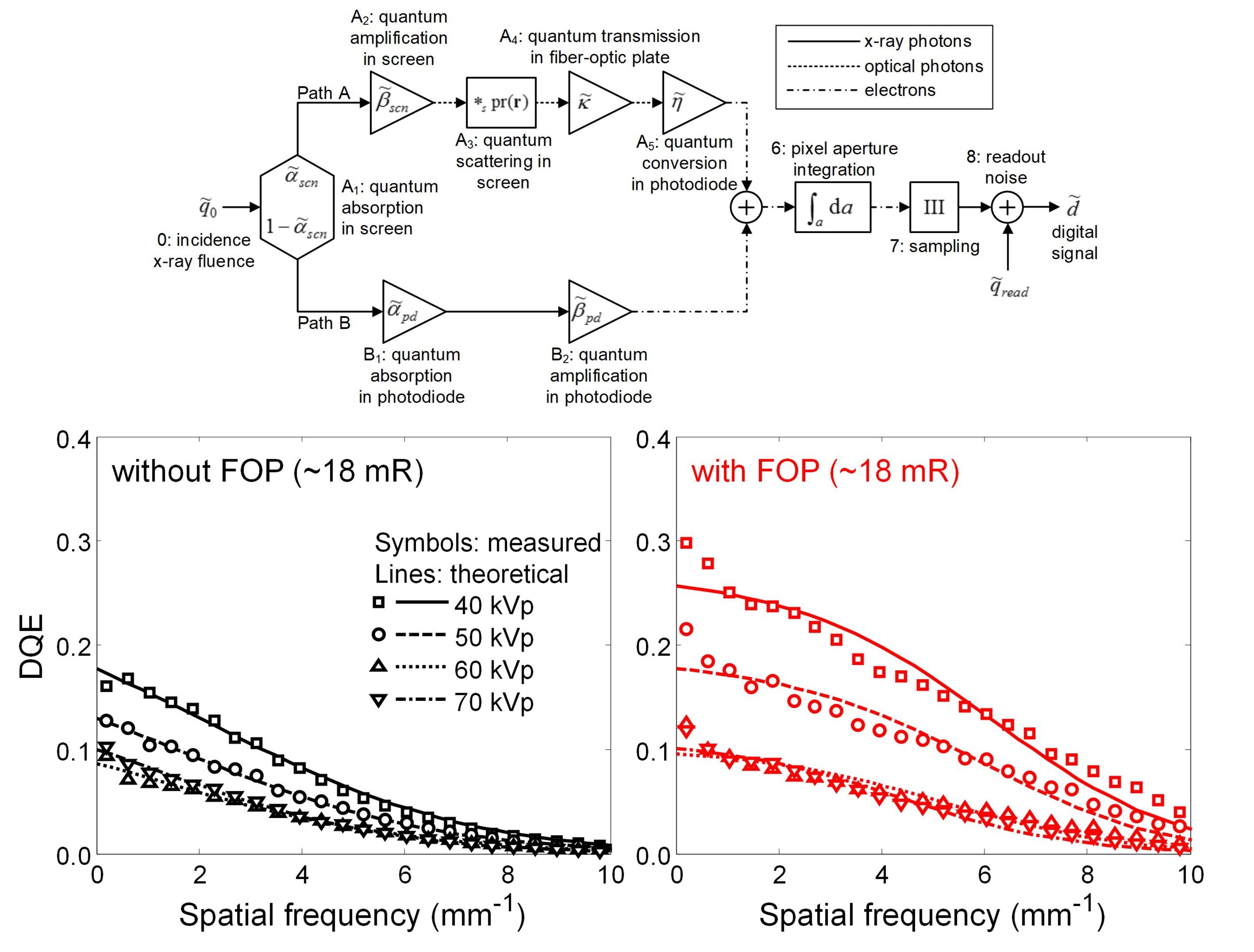
[1] D. W. Kim, J. C. Han, S. Yun, and H. K. Kim, “Aging of imaging properties of a CMOS flat-panel detector for dental cone-beam computed tomography,” J. Instrum. 12, p. P01005, 2017.
This work was supported by the National Research Foundation of Korea (NRF) grant funded by the Korea government (MSIP) (No. 2021R1A2C1010161).
Corresponding author: hokyung@pusan.ac.kr
Quality assurance of many electronic parts, such as lithium-ion batteries, semiconductor packages, and multilayered printed circuit boards (PCBs), requires an exhaustive defect inspection procedure. Computed tomography may be the best non-invasive technique for identifying tiny defects inside products. Considering the geometries of the products to be investigated, the data (projections) acquisitions over 180$^{\circ}$ are sometimes unsuitable. The conventional filtered backprojection (FBP) works under the Fourier slice theorem, and the complete data-filled Fourier space guarantees the FBP-based image reconstruction. However, the limited data or angle tomography generates the null space in the Fourier domain, which causes artifacts in the reconstructed images [1]. In addition, since the FBP algorithm is based on a continuous function, which does not match the acquired projections that are discrete data, the FBP is vulnerable to noise and prone to produce artifacts.
Iterative reconstruction (IR) starts from the discretized model ($A\mathbf{x}=\mathbf{b}$) that incorporates the data ($\mathbf{b}$) that is available. Therefore, the reconstructed image ($\mathbf{x}$) is relatively robust to noise and artifacts. Moreover, IR can be applied to any scanning trajectories by properly designing $A$, which describes rays from the x-ray source through the object to the detector pixels. The recent availability of large computational capacities and their progressive improvements push the replacement of FBP by IR.
In this study, we apply various IR algorithms to the limited angle tomography of PCBs and investigate their feasibility in comparison with FBP. The investigating IR algorithms include the algebraic reconstruction technique (ART), ART with total-variation regularization, statistical reconstruction with the maximum likelihood expectation maximization (ML-EM) algorithm, and least-squares reconstruction with conjugate gradient algorithm (CGLS). Example results are shown in the figure attached to this abstract. We describe the algorithmic differences in detail and discuss their similarities and differences quantitatively.
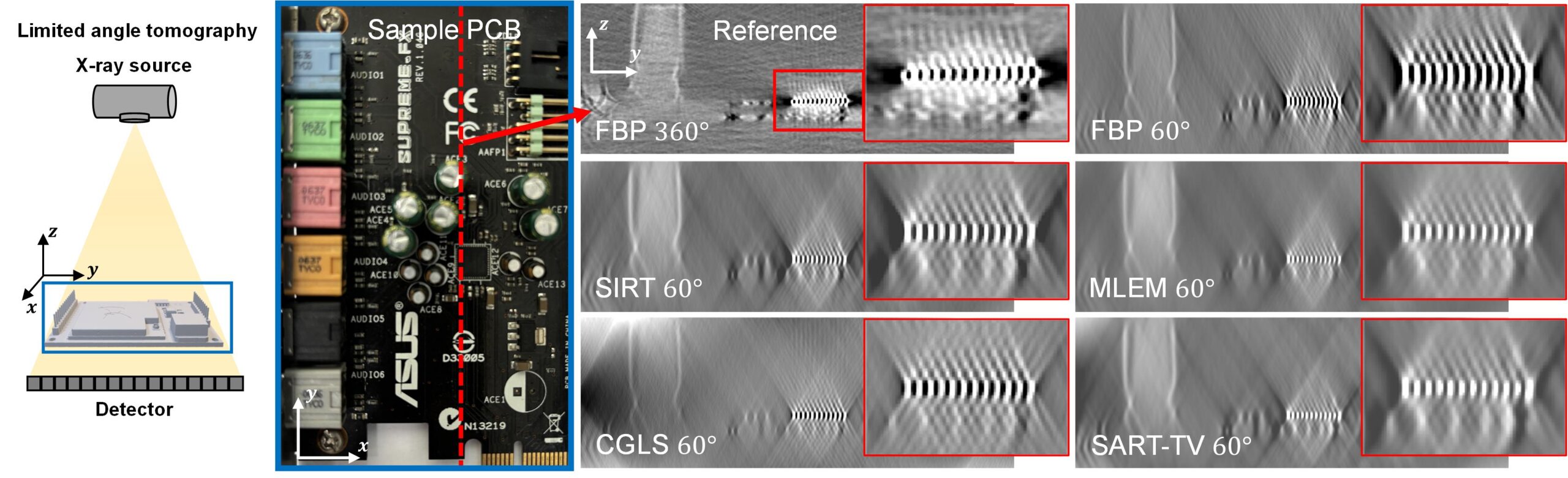
[1] H. H. Barrett, “Limited-angle tomography for the nineties,” J. Nucl. Med. 31(10), pp. 1688–1692, 1990
This work was supported by the National Research Foundation of Korea (NRF) grant funded by the Korea government (MSIP) (No.2021R1A2C1010161).
Corresponding author: hokyung@pusan.ac.kr
The High-Intensity Heavy-ion Accelerator Facility (HIAF) is a leading platform for heavy ion scientific research in China with advanced beam current indicators. Several physics experiments such as the Electron-ion collider in China (EicC), the China Hyper-Nuclear Spectrometer (CHNS), the High energy FRagment Separator (HFRS) are being under construction at HIAF. To measure the position, energy deposition, and arrival time of particle hit in these experiments, Low-Gain Avalanche Detectors (LGAD) have become the detector of choice due to an excellent performance. The readout circuit of LGAD requires time-to-digital converters (TDC) to convert the time measurement results into digital signals. Thus, the performance of TDC is crucial for the readout circuit. Since smaller pixel area is conducive to improving positional resolution and spatial resolution, a TDC using a calibration module instead of DLLs is proposed to achieve lower power consumption and area.
The proposed TDC is a 3-stage architecture, the first stage uses a high-speed counter TDC, achieving a large dynamic range; the second stage is a delay-line TDC, which balances between the dynamic range and resolution; the last stage is a vernier delay-line TDC, achieving a high resolution. The 3-stage architecture achieves both large dynamic range and high resolution. In addition, a calibration module is used to measure the relationship between two adjacent stages of resolution, thus, the resolution of the TDC could be confirmed under the influence of PVT variation. Compared with the TDCs using DLLs, the proposed TDC reduces the power consumption and area.
The resolution of TDC is about 5.13 ps, and the dynamic range is 25.2 ns. The INL and DNL are both less than 0.3 LSB. Including two TDCs which measure the TOA and TOT respectively, the layout area is 931*447 μm2.
In general, the principle of the X-ray transmission imaging system used for container inspection involves irradiating an object with high-energy X-rays and measuring the extent to which the rays penetrate through the object.
However, due to their high penetration capability, high-energy X-rays encounter difficulties in detecting low-density substances such as narcotics (powder) and explosives. In this study, we propose developing an X-ray backscatter imaging system to inspect low-density hazardous materials within containers.
The development system utilizes X-rays with an energy of 225 keV and rotates a wheel collimator to scan the container's three sides (top, left, right) with a point beam.
The image detector, which consists of 12 scintillation detectors, uses the synchronization signal from the rotating wheel collimator to simultaneously collect backscattered X-rays produced by the Compton effect, thereby generating line images.
Finally, each generated line image is displayed as a composite image.
We constructed a gantry-type inspection system with X-ray backscatter imaging technology applied within a testbed and performed scans of actual vehicles to generate backscatter images.
This work presents a comprehensive study on the development of a sophisticated gamma radiation detection system tailored for aerial mapping and radiation surveillance, which is to be used to generate an environmental radioactivity map within the United Arab Emirates (UAE). To optimize detection sensitivity, the project incorporates careful assembly and calibration techniques that make use of four high-resolution crystals (two Cebr3 and two LBC crystals). The use of crystals with elevated intrinsic background radiation levels (LBC) is to evaluate their suitability for the detection task. At the same time, we study how well a VETO system works to improve signal-to-noise ratio and lower background noise. Modern front-end and back-end electronics are used in the detector system to digitize the signal at the outset of signal processing. In order to facilitate thorough and effective surveys, the detector will be installed on a drone. The system will also incorporate AI-driven algorithms and real-time communication capabilities for effective data processing.
Taking these factors into account, our research and development (R&D) project seeks to improve the capabilities of airborne radiation monitoring systems by optimizing a drone-mounted gamma scintillation detector designed for mapping, surveillance, and search operations
The Heavy Ion Research Facility in Lanzhou (HIRFL) and the High Intensity heavy-ion Accelerator Facility (HIAF) are essential platforms for heavy-ion scientific research in Asia. Some experimental facilities are currently under construction at HIRFL and HIAF, such as the CSR External-target Experiment (CEE), the High energy FRagment Separator (HFRS), the China Hyper-Nuclei Spectrometer (CHNS), and the Electron-ion collider in China (EICC). These projects aim to enhance advanced experimental conditions for research in heavy ion physics and related interdisciplinary fields. In the context of large-scale scientific experimental facilities, as the collision energy increases rapidly, detector resolution improves, and trigger-less readout is implemented, higher demands have been proposed on the radiation resistance and transmission speed of the signal transmission links.
The advent of high-speed serial data transmission technology has significantly enhanced the transmission speed of links. A clock and data recovery (CDR) circuit can extract the clock information from high-speed serial data, and recover the clock to sample optimally at the center of a unit interval (UI), improving the quality of data transmission in physical experiments. Thus, a quarter-rate radiation-resistant CDR has been designed for large-scale physical experiments. The proposed CDR is based on a phase interpolation structure, consisting of a phase interpolator, eight high-speed samplers, two 4:120 Deserializers, a Bang-Bang phase detector, and a digital loop filter. The two-level structure phase-interpolator effectively enhances the precision of the interpolation clock. The customized three-level structure in the Deserializer guarantees the timing margin between the data and the clock. The pipeline-structure digital loop filter increases the data throughput rate of digital circuits. Furthermore, various strategies are considered to reduce the impact of radiation on the chip, such as triple-mode redundancy technology, modular design method, and reasonably modifying the layout of critical nodes.
The proposed CDR is designed in a 55 nm process and the input data rate is 20 Gbps. Ultimately, the bit error rate (BER) of the CDR is lower than 10e-12 and the power is less than 180 mW with a supply voltage of 1.2V.
In the field of clinical Computer Tomograpy(CT), the application of photon-counting detectors(PCDs) is expected to have large potential to bring the next breakthrough for the industry. In recent years, a small number of companies has developed Photon Counting CT(PCCT) prototype scanners equipped with direct-conversion PCDs based on room-temperature semiconductors, such as Silicon, CdTe and CdZnTe (CZT). These room-temperature semiconductors are considered as the most promising materials for PCDs in PCCT. However, specific drawbacks of these direct-conversion detectors are in evidence, such as the occurrence of charge sharing and charge trapping, leading to increasing of the image noise and unstable detector operation state. In addition, high purity semiconductor wafers with a very low defect concentration are required in fabrication process of PCDs, which may negatively affect the cost-effectiveness of production. In this work, we introduced a scintillator-based detector coupled with the CMOS-based photosensor, as an alternative detector technology roadmap for the PCCT medical imaging applications.
To study the feasibility of the scintillator-based PCD, we develop a Monte Carlo simulation framework for the detector evaluation. The framework includes the simulation of detector and ASIC. In the detector simulation, we took into account of the X-ray interactions with detector bulk material, as well as the optical process. In the signal processing simulation of the ASIC, there have a charge sensitive amplifier, a high pass filter and photon counting modules. We subsequently use the framework to compute the expected energy spectrum of a CeBr3-based PCD prototype with sub-mm pixel sizes. According to the experimental result, CeBr3 crystal have a density of 5.1g/cm3, a high light yield of 60000/MeV and a fast scintillation decay time of 20ns. According to the reconstructed spectrum, the scintillation-based detector shows lower energy resolution than the semiconductor-based detector with a same pixel size, but also less the K-edge escaping photon contributions from the adjacent pixels in the spectrum. An analysis of the variance Cramer-Rao Lower Bound(CRLB) in basis material decomposition of single detector pixel is finished with the simulation result. According to our primary estimation, the scintillator-based detectors is proved to have comparative performance of CRLB to Si and CZT detector under a X-ray flux of 50Mcps/mm2.
According to this study, scintillator materials with better energy resolution and faster decay time can significantly improve the CRLB performance of the detector system. In our next plan, more in-depth research will be performed to validate the practical utilization of this technical method, including the material uniformity, hygroscopic property, scintillation property, detector dicing and encapsulation. This work provides evidence that it may be feasible to develop scintillator-based detectors for PCCT that can compete with CdTe and CZT detectors under lower X-ray flux.
Recently, the measurement of gamma-rays polarization has increasingly become important for applications in various fields such as astrophysics measurements and medical imaging. One common method of gamma-rays polarization measurement is utilizing the formula of differential cross section in Compton scattering, $dσ⁄dφ=A+Bcos(2φ)$, where $φ$ represents the scattering azimuth angle from polarization direction of gamma-rays, and others are constant values. In this study, we fabricated the gamma-rays polarization detector using $\mathrm{Gd_3(Ga,Al)_5O_{12}(Ce)}$ scintillator, in short GAGG, and measured the gamma-rays polarization in MeV range based on this method, assessing modulation and accuracy of this detector. The detector mainly consists of scatterer and absorber, each of which use GAGG array. This GAGG array is pixelated 8×8 with a single pixel size of 2.5 mm × 2.5 mm and a pitch of 0.7 mm. We used 1 piece of GAGG array with 4 mm thickness for scatterer, and 8 pieces with 9 mm thickness for absorber, and attached Multi-Pixel Photon Counter (MPPC) array on each GAGG array. In order to detect scattering azimuth angle, these 8 set of GAGG-MPPC arrays in absorber were placed 5 cm away from the scatterer in a circular pattern parallel to it. For polarized gamma-rays irradiation to scatterer, we used B1LU beamline in Ultraviolet Synchrotron Orbital Radiation Facility (UVSOR) with 6.6 MeV energy, which can control gamma-rays polarization. We irradiated 0°, 45°, 90°, and circular polarization gamma-rays to the center of the scatterer and acquired data on energy and location from MPPC via our FPGA and electric circuit system. Then we calculated the scattering azimuthal distribution and fitted with cosine function. As a result, the modulations, defined as $(N_{max}-N_{min})/(N_{max}+N_{min})$, for 0°, 45°, 90° polarization were respectively 2.85%, 2.48%, 2.84%, which were close to the simulated result in Geant4, 1.71%, 1.59%, 1.94%. Also, we got relatively low phase errors from theoretical values as 4.11°, 4.19°, 13.2°. In summary, developed detector successfully detects the gamma-rays polarization and shows potential for the application especially in MeV range.
A new single photon-counting ASIC called UFERI (Ultra-Fast Energy Resolved Imager [1]) is under development by the ASIC design group of AGH University and the detector group of the SOLEIL synchrotron. The detector is dedicated to pseudo-Laue diffraction applications in intense, pink beams at synchrotrons. The prototype consists of 42×42 pixels with a pitch of 75 µm, each containing a charge-sensitive amplifier with gain control, three discriminators, and corresponding counters. With its three thresholds, UFERI can discriminate multiple energy levels, and its short dead time ensures a high count rate capability of up to 23 Mcps/pixel (30% dead time loss). In addition, UFERI has a zero-dead time readout mode, and three independent gates for the three discriminators which, combined with a short gating time, allow for ultra-fast pump-probe-probe experiments. In low-noise operation mode, a capacitor discharge technique [2] implemented on-chip allows to alleviate the trade-off between noise and count rate performance, enabling operation with an ENC much below 100 e- rms, while accepting a moderate photon flux above 1 Mcps/pixel.
This proposed poster will describe the architecture of the ASIC (see Fig. 1) and present the main results of the characterization. We will show the energy calibrations, threshold dispersions, and gain spread, as well as the count rate and timing performance of the UFERI (see Fig. 2).
[1] F. Orsini, A. Dawiec, B. Kanoute, P. Grybos, R. Kleczek, P. Kmon and P. Otfinowski, “Ultra-Fast Energy Resolved Imager for `Pseudo' Laue diffraction experiments at synchrotron facilities”, Journal of Instrumentation, vol. 19, no. 02, p. C02055, 2 2024.
[2] R. Kleczek, P. Kmon, P. Maj, R. Szczygiel, M. Zoladz and P. Grybos, “Single Photon Counting Readout IC with 44 e-rms ENC and 5.5 e-rms Offset Spread with Charge Sensitive Amplifier Active Feedback Discharge”, IEEE Transactions on Circuits and Systems I: Regular Papers, vol. 70, no. 5, pp. 1882-1892, 5 2023.
In our presentation, we delve into the investigation of the inter-pad (IP) region within double trench isolated LGADs (2Tr TI-LGADs), focusing on double-trenched PINs from both the RD50 and AIDAInnova production runs. Our previous research revealed that exceptionally large signals, with prolonged duration, manifest in the IP region alongside the standard IP signals recorded in conventional LGADs with 2JETs and 2 p-stops. We have identified a correlation between strong signals and ghost signals persisting in the IP region even when the laser is deactivated. Recently, we replicated a study using double-trenched PINs (without gain layer in pads) and observed no ghost signals. However, under specific laser power and bias threshold conditions, we recorded remarkably high signals with prolonged duration, akin to observations in double-trenched LGADs where ghost signals were present. This prompted us to conduct a systematic study to explore the relationship between laser threshold and bias, aiming to establish the threshold for charge accumulation between trenches that trigger the ghosts. We discovered that the laser power needed to replicate a strong signal akin to one observed in LGADs (with ghosts in the IP region) was significantly higher in the PIN sample from AIDAInnova than in the PIN sample from the RD50 Common project production; this difference was significantly higher at higher bias Additionally, we conducted an identical study on double-trenched LGADs from AIDAInnova, where the gain layer is carbon-enriched, and the guard ring is differently designed compared to double-trenched LGADs from the RD50 common run. The measured bias threshold at which ghost signals are triggered in the IP region of the device from AIDAInnova was significantly lower than in the sample from the RD50 Common project. These peculiarities motivated us to undertake comprehensive studies to elucidate the observed differences among sensors. In this presentation, we will provide a concise overview of the main finding and offer an interpretation.
Locating radioactive hot spots presents a challenge for the nuclear industry and security applications, such as waste management, decommissioning, radiation protection, and the management of nuclear accidents. Detection of fast-neutron emission offers an alternative technique to gamma imaging for verifying the location of radioactive materials. In this study, we present a prototype of gamma-neutron imager utilizing a 12 × 12 plastic scintillator (PS) pixel matrix, with each pixel measuring 3.6 mm × 3.6 mm × 3.6 mm and coupled to a silicon photomultiplier (SiPM). The light response of each pixel is separated by 0.6 mm of PTFE wall. The electronic readout includes the ArrayC-30035-144P SiPM from SensL, Cork, Ireland, connected to the diode-coupled charge division readout from AiT. We utilized a rank 7 MURA coded aperture, comprising two layers: 1 mm of lead and 1 cm thick polyethylene, with a surface area of 11.4 cm × 11.4 cm. This aperture is positioned 5 cm away from the detector and with this setup, the prototype has a field of view (FoV) of 68°. Additionally, all components were assembled within a polyethylene camera housing measuring 17 cm × 14 cm × 9 cm.
We performed Geant4 simulations to determine the optical parameters of the scintillator, explore quenching mechanics, and examine neutron interactions within our scintillator. The simulation framework was validated using experimental results. Additionally, we conducted tests on the prototype using a proton beam at the Cyrcé facility at IPHC, employing a CMOS MAPS sensor to evaluate the beam profile. In this talk, we will discuss the simulation results, comparing them with the experimentals outcomes. Moreover, we will illustrate the spatial resolution capability of the prototype and present our calibration study on its energy response, using both simulation and test results.
Keywords: Neutron imaging, Pixelated plastic scintillator
(PS), silicon photomultiplier (SiPM), Geant4, Cyrcé facility
The semi-insulating (SI) bulk GaAs has been studied as a material for semiconductor detectors operating at room temperature for decades, exhibiting good gamma and X-ray detection efficiency and stability during its operation. Moreover, its high carrier mobilities up to 8000 and 400 cm2V–1s–1 for electrons and holes, respectively at room temperature ensure high counting rate of SI GaAs detectors. Furthermore, their confirmed high radiation hardness predetermines their use in harsh environment or for long-term operation in space applications. However, in comparison to traditional semiconductor detectors based on silicon, the bulk SI GaAs detectors suffer from worse spectrometric properties like charge collection efficiency (CCE) or energy resolution. These parameters are affected by the base material quality and the intensity of electric collecting field in the detector volume, which is controlled by the applied bias and detector electrodes. It has been shown, that the CCE increases with the applied bias, but it saturates to the certain value depending on the GaAs detector thickness. A thicker detector achieves a lower maximum CCE and vice versa, for both, the alpha and gamma spectrometry [1]. In the case of bulk undoped SI GaAs detectors, we have achieved the highest CCE of about 80% for 230 µm thick Schottky barrier type detectors.
Reducing the substrate thickness while preserving the area of detector will improve the spectrometric properties. However, the GaAs substrate preparation technology prevents the production of SI GaAs wafer thinner than 200 µm, mainly due to its fragility.
At the Institute of Electrical Engineering, SAS in Bratislava, the technology of preparing SI GaAs detectors with a thickness in the range from 60 um up to 200 um was developed, using the wet chemical etching method. The prepared detectors have circle Schottky electrode of 0.5 mm in diameter on the top side based on Ti/Pt/Au metallization and the full area Ni/AuGe/Au ohmic electrode on the etched bottom substrate. First, the current-voltage characteristics of prepared detectors were measured, showing saturation current in the range of a few nA. Then, the prepared detectors were tested with triple 239Pu238Pu244Cm alpha particle source in vacuum to determine their CCE and energy resolution. The spectrometric chain based of Cremat charge sensitive preamplifier and a Caen Hexagon digital pulse shape amplifier was utilized. The best achieved energy resolution was about 80 keV @ 5.5 MeV alpha particles obtained with the thinnest (60 um) SI GaAs detector, which reached also the best CCE of 91% saturating at bias higher than 45 V. The detectors with such improved CCE enabled to experimentally determine the lifetime of electrons in SI GaAs and thus characterize its quality.
[1] A. Sagatova et al. EPJ Web of Conferences 288, 10013 (2023)
Acknowledgement: This work was partially supported by grants of the Slovak Research and Development Agency Nos. SK-CZ-RD-21-0116 (CZ no. LU-ASK22147), APVV-22-0382, APVV-18-0273.
The interaction of an electron with the dipole field of a neutral atom or molecule can lead to radiative photon emission by analogy with the familiar case of Nuclear Bremsstrahlung. This process is referred to as Neutral Bremsstrahlung and is possible even in noble atoms due to their induced dipole moment. Neutral bremsstrahlung in noble gases has been neglected in favor of excimer-based Vacuum-Ultraviolet emission, being only recently studied in argon and xenon. In this study, we present preliminary results of the neutral bremsstrahlung emission spectrum obtained experimentally in pure argon at 1.2 bar, covering the 150–550 nm wavelength range, and under reduced electric fields within the 0–2 kV/cm/bar range.
EMPIX2 is a novel hybrid pixel detector readout ASIC for electron microscopy with a maximum frame rate of 100 kfps and a very large dynamic range[1]. It features 128 x 128 square pixels at a pitch of 150 um. The ASIC was bump bonded to 500 m thick silicon pixel sensor and tested.
Based on the EMPIX2 detector testing system, we designed and assembled a prototype camera for electron microscope. it is mounted on a TECNAI F20 electron microscope (see Fig.1) and we did lots of experiments to evaluate the performance of the camera. Currently, limited by the data acquisition system, this camera can operate stably at half the highest frame rate, that is 50 kfps. In TEM mode, a flat field beam is used to vertically illuminate the camera, and the gain and offset of the detector are corrected pixel by pixel through scanning the exposure time to compensate the inconsistency of each pixel.
After completing the calibration of the gain, we test the detector response to low-dose electrons, and the results showed that it has good single electron resolution. Through edge imaging, we obtain the MTF and DQE of the detector. Fig.2 shows flat-filed images of a pin, the edge of the pin is clear. We are conducting more experiments and expect to display more electron microscopy images of some typical materials or samples.
HiZ-GUNDAM is a future satellite mission for gamma-ray burst observations, designed to detect X-ray transients with the wide-field X-ray monitor, and to perform automatic follow-up observations with the near-infrared telescope. The wide-field X-ray monitor consists of an X-ray optical system, Lobster Eye Optics (LEO) and pnCCD imaging sensor to monitor a wide field of view (FoV) of ~0.5 steradian at 0.4-4.0 keV.
LEO is soft X-ray focusing mirror, which is an innovative X-ray optical system that provides both a wide field of view and high sensitivity. It has a spherically curved SiO2 plate with millions of micropores, and inside of pores are coated with heavy metals. It reflects and focus soft X-rays and making the cross image on focal plane. Compared to the current mainstream coded mask method used in astronomical satellites, mirror optics like LEO can efficiently focus and reduce the effect of cosmic X-ray background. That makes possible to achieve an improvement in sensitivity of more than one order of magnitude. The LEO segments can be expanded its FoV by arraying and aligning multiple LEO segments on a spherical shell.
We developed an optical frame as a breadboard model (BBM) to set 9 LEO segments manufactured by Photonis Co. Ltd. on the spherical shell. Each segment measures 4 cm × 4 cm, and the cross image size at the focal plane is 2 cm × 2 cm, with a distance of 30 cm from LEO. The detector system combining the optical frame with a CMOS image sensor was constructed, and its X-ray performance has been tested. The tests focused on key parameters such as angular resolution, effective area, and angular response of the LEOs. In addition, vibration tests simulating launch of locket were conducted on the BBM frame with LEO to assess the structural characteristics of the system. We investigated the characteristic frequencies of the BBM frame and the response for random vibration. In addition, we performed further vibration tests for the BBM housing combined with the BBM frame, and investigated the structural properties of the entire detector system of the wide-field X-ray monitor.
We will report detailed X-ray performance and structural properties of the wide-field X-ray monitor with Lobster Eye Optics.
Electroluminescence (EL) describes the scintillation emission by a material upon electron impact under an external electric field. Gas Proportional Scintillation Counters (GPSC) relay on EL produced in noble gases to amplify the ionization signal coming from the radiation interaction with the gas medium. Various detector geometries have been proposed for this type of detector, the most common using two parallel meshes to define the EL region with an uniform electric field. However, the dependency of the solid angle subtended by the photosensor relative to the EL emission position, thus on the primary electrons position and, consequently, on the radiation interaction position limits the GPSC window size when compared to the photosensor active area. This study proposes an annular EL region with an azimuthal geometry in respect to the photosensor to maintain constant the referred solid angle, facilitating the use of large radiation windows. Other advantages of this design are the simplicity of the GPSC construction, in respect to other solutions: only an annular anode, having its axis aligned with the photosensor axis, will be needed to bias the GPSC. Experimental results demonstrate good energy resolution for 5.9, 22.1 and 56.4 keV, and the capability of having a six times greater radiation window area compared to the 2 $cm^{2}$ sensitive area with an LAAPD as the photosensor. Simulation studies, using dedicated software for the primary charge generation, drift and diffusion, photon emission due to the increasing electric field and light propagation and collection in the photosensor, are also presented. These results corroborate experimental findings, highlighting the detector's viability for x-ray astronomy applications as a portable, room-temperature device with a large detection area and volume, rivaling solid-state detectors.
Keywords: Electroluminescence ● Gas detectors ● Scintillation counters ● X-ray
Detectors ● GPSC ●
The TUPI (Timepix-based Ultra-fast Photon Imaging) direct conversion hybrid detector, currently under design at the SIRIUS light source, is a modular photon-counting detector based on the Timepix4 ASIC (Application Specific Integrated Circuit). It targets multiple SIRIUS bioimaging beamlines for ORION, Brazil’s first Biosafety Level 4 (BSL4) laboratory under design. Each TUPI base module will be composed of a set of 3x1 ASICs that can be bump-bonded to different sensor materials depending on the beam energies, providing an active area of approximately 75 x 28 mm² (1344 x 512 square pixels of 55 μm pitch). Its modular design approach ensures scalability for larger active areas. With accompanying mechanics, cooling, power supply, digital control, and multigigabit transceivers, each module can stream thousands of frames per second through 48x10.24 Gbps optical links directly connected to a DAQ server. The ASIC’s control and configuration are managed by a control board featuring an Ethernet interface for external communication and an FPGA for deterministic tasks. The TUPI’s detector head design is extremely compact and specified to be vacuum-compatible. This work will discuss conceptual front-end electronics design, highlighting challenges and future development.
Timepix2 [1] is a hybrid pixel detector developed by the Medipix2 collaboration as the successor to Timepix [2]. Its release introduced significant enhancements, including simultaneous measurement of Time-over-Threshold (ToT) and Time-of-Arrival (ToA), along with additional features such as adaptive gain mode and pixel disabling to reduce chip power consumption. These latter features, coupled with an occupancy trigger and compact size, enable the use of Timepix2 for space dosimetry applications, where high-energy heavy ions (such as Galactic Cosmic Rays) can deliver substantial radiation doses to humans and electronics, potentially causing upsets. The improved pixel-level energy measurements also facilitate dE/dX spectroscopy in space using Timepix2.
In this contribution, we present the study of the response of a Timepix2 (v1) detector (256 × 256 pixels, pixel pitch 55 μm) with a 500 μm thick silicon sensor in charged particle beams of relativistic ion fragments at the Super-Proton-Synchrotron at CERN. This mixed field was created by a 385 GeV/c primary lead beam interaction in a beryllium target The detector was configured in adaptive gain mode, providing a larger per-pixel energy range, and irradiated at different angles.
Prior to the testbeam campaign the Timepix2 detector was calibrated using previously developed methodology [3] using protons with energies in the range from 400 keV to 2 MeV and α -particles of 5.5 MeV from 241Am source. Measuring at different bias voltages allows for varying the energy deposition in single pixels. In contrast to the findings of the previous work, where Timepix2 saturated at ~2.6 MeV [3], it was found that the Timepix2 chip (v1) studied in the present work shows a linear response at least up to 3 MeV deposited per pixel energy in adaptive gain mode. To further understand this issue, the temperature dependence of the Timepix2’s energy response will be investigated and discussed.
We present and discuss energy deposition spectra for relativistic particles of different stopping power. The main goal of the deposited energy spectra analysis is investigation the capabilities of the Timepix2 detector for decomposing the mixed beam. Using spectrum stripping technique by iterative Landau curve fitting charge discrimination could be done up to Z = 13 (see figure 1) for impact angle of 70 degrees with respect to the sensor normal. Timepix3 results, for example, indicated sensitivity up to Z=7 [4]. Using the acquired test beam data, we will further refine the per-pixel energy response determined with above described methodology and compare it to the electronics design simulations from [1].
References:
[1] W.S. Wong et al., 2020 Radiat. Meas. 131 106230.
[2] X. Llopart et al., NIM A 581 (2007) 485–494.
[3] B. Bergmann et al., 2022 JINST 17 C01025.
[4] Smolyanskiy et al., 2021 JINST 16 P01022.
Acknowledgements:
B.B. and P.S. acknowledge funding from the Czech Science Foundation (GACR) under Grant No. GM23-04869M.
Data compression is becoming a critical necessity for high throughput synchrotron radiation experiments like Computed Tomography (μ-CT), where the bit depth, data rate, and detector size continue to increase, contributing to the so-called “data deluge” [1]. Previous studies of data compression frameworks for μ-CT based on JPEG-XR [2] highlighted that lossy methodologies can be a suitable alternative [3,4] to lossless ones. However, the limitation of certain codecs to operate only on integer data may pose a challenge for detector systems, particularly those integrating edge-computing capabilities (e.g. averaging/combining exposures, de-noising, calibration, HDR frames).
This work focuses on the perceptual evaluation [5,6,7] of lossy data compression techniques designed specifically for X-ray tomography; following the steps of medical imaging [5,6], we investigate data compression for μ-CT using modern perception-based quality metrics such as 4-MS-G-SSIM [5] and HDR-VDP3 [7] (applied end-to-end) which have been proved to be “good surrogates of a radiologist” [5]. By comparing these metrics with a loss function based on Fourier Ring Correlation (FRC) [8], a quantitative measure commonly used to estimate resolution in computational imaging, we aim to bridge the gap between visual quality metrics and quantitative measures like FRC. Additionally, we extend previous studies by evaluating the efficacy of compression techniques on floating-point 32-bit data, to accommodate for future detector requirements and advanced pre-processing.
Fig 1. Comparison of 4-MS-SSIM (green curve) and FRCLoss (red curve) computed on the reconstruction of a kettocarbonate μ-CT dataset (open data available at [9]) (panel a) as a function of the quantisation factor Q, which is an integer parameter [0-255] of the jpeg-xr encoder [10]. The Q parameter, controls the balance between image quality and file size (0: no compression, 255: maximum compression). Notably, both metrics exhibit the same trend, particularly evident at the knee point where they both reach 0.9 (point A) for Q = 150 (nearest computed value). Comparing the corresponding file sizes (point B, intercept with the compressed file size curve – blue), the compression is of a factor of 14. The other panels show (for the same Q value) respectively: the decompressed sinogram (b), the rawdata – compressed difference (c), the reconstructed slice (d) and its difference with the ground truth (e) [9].
REFERENCES:
[1] R. Rao, “Synchrotrons face a data deluge,” Physics Today, vol. 2020, no. 2. AIP Publishing, p. 0925a, Sep. 25, 2020, http://dx.doi.org/10.1063/PT.6.2.20200925a
[2] L. Mancini et al., “About a method for compressing x-ray computed microtomography data,” Measurement Science and Technology, vol. 29, no. 4. IOP Publishing, p. 044002, Mar. 08, 2018. doi: 10.1088/1361-6501/aaa0fa. Available: http://dx.doi.org/10.1088/1361-6501/aaa0fa
[3] F. Marone et al., “Impact of lossy compression of X-ray projections onto reconstructed tomographic slices,” Journal of Synchrotron Radiation, vol. 27, no. 5. International Union of Crystallography (IUCr), pp. 1326–1338, Jul. 28, 2020, http://dx.doi.org/10.1107/S1600577520007353
[4] F. Alted et al., Blosc2, Grok and JPEG2000, online https://github.com/Blosc/leaps-examples
[5] G. P. Renieblas et al., “Structural similarity index family for image quality assessment in radiological images,” Journal of Medical Imaging, vol. 4, no. 3. SPIE-Intl Soc Optical Eng, p. 035501, Jul. 26, 2017, http://dx.doi.org/10.1117/1.JMI.4.3.035501
[6] K. J. Kim et al., “A Comparison of Three Image Fidelity Metrics of Different Computational Principles for JPEG2000 Compressed Abdomen CT Images,” IEEE Transactions on Medical Imaging, vol. 29, no. 8. Institute of Electrical and Electronics Engineers (IEEE), pp. 1496–1503, Aug. 2010, http://dx.doi.org/10.1109/TMI.2010.2049655
[7] R. K. Mantiuk et al., “HDR-VDP-3: A multi-metric for predicting image differences, quality and contrast distortions in high dynamic range and regular content.” arXiv, 2023, https://arxiv.org/abs/2304.13625
[8] N. Banterle et al., “Fourier ring correlation as a resolution criterion for super-resolution microscopy,” Journal of Structural Biology, vol. 183, no. 3. Elsevier BV, pp. 363–367, Sep. 2013, http://dx.doi.org/10.1016/j.jsb.2013.05.004
[9] A. Singh et al., “On Representative Elementary Volumes of Grayscale Micro‐CT Images of Porous Media,” Geophysical Research Letters, vol. 47, no. 15. American Geophysical Union (AGU), Aug. 07, 2020, http://dx.doi.org/10.1029/2020GL088594
[10] JPEG-XR reference code, online https://jpeg.org/downloads/jpegxr/jpegxr-ref.zip
The HEXITEC 2×6 Instrument has been developed for the National X-ray CT (NXCT) Centre’s Colour X-ray bay at the University of Manchester. A single HEXITEC ASIC is typically bonded to a 2×2cm CdZnTe, CdTe or other High-Z material and readout by the HEXITEC GigE system. However, with an increasing demand for large area high energy detectors we have employed the use of tiled arrays of 2×6 ASICs. The HEXITEC 2×6 is made of twelve 2mm thick High Flux CdZnTe sensors supplied by Redlen Technologies Inc. mounted in a 2×6 array resulting in 76.8k fully spectroscopic pixels, operating from 3-180keV with 1keV FWHM energy resolution and a 48cm2 active area. Each individual sensor consists of 80×80 pixels on a 250um pixel pitch.
The HEXITEC 2×6 has been designed as a compact system allowing it to be used flexibly for a large range of experimental setups in the dark or bright field, with the entire system measuring 1750×2400×950 mm. HEXITEC runs at 9kHz with readout performed row by row in four parallel blocks of 20×80 pixels per ASIC. Modular readout boards digitise ASIC outputs into 16-bit values which are received by an FPGA board. Incoming data streams are converted into 160×480 pixel frames and 10G ethernet packets. 2 × 10G SFP interfaced data lanes send odd and even frames to the control PC with a total raw data rate of 15Gbps. The control and data receiving and processing is conducted using ODIN, which can be integrated with the EPICS software used at many large science facilities.
In this paper we will present the technical design and operation of the camera followed by a characterisation of the overall performance under X-rays. Additionally, we will discuss results from the CdZnTe with a focus on spectral performance and spatial uniformity.
Designed to function as the primary tracking detector for the future CBM experiment at FAIR, the Silicon Tracking System (STS) is tailored to measure charged particles generated during heavy-ion collisions at unprecedented interaction rates of up to 10 MHz, using a triggerless free-streaming readout approach. The detector modules developed for STS integrate large-area double-sided silicon sensors, lightweight high-density interconnecting microcables, and a custom-designed self-triggered readout ASIC. This configuration results in modules with low material budget capable of providing 2D position information alongside timing and amplitude data.
Central to the STS project is the series production of detector modules and ladders, which also involves assembly and quality control measures for each component. A comprehensive functional and thermal stress testing of the finalized modules ensures their reliability before their integration onto carbon-fiber ladders. Beyond that, the operational capabilities of STS modules are evaluated in various application scenarios. High-intensity nucleus-nucleus collisions at GSI facilities and the E16 experiment at J-PARC serve as platforms for evaluating their performance.
This report provides a detailed overview of the production processes involved in STS module fabrication, along with results from functional module testing, and insights gained from their operational deployments across distinct experimental setups.
The Large Hadron Collider (LHC) is going to enter a High Luminosity – LHC(HL-LHC) phase with a 6-time higher instantaneously luminosity. The increased number of interactions per bunch crossing (pile-up) is one of the experimental challenges in the front-end readout design because a much faster recovery time to the baseline (< 25ns) is required. Depleted Monolithic Active Pixel Sensors (DMAPS) draw a lot of interests to be used as a sensor for timing in High Energy Physics experiments for its advantage of integrating the sensor and the electronics on the same substrate that saves effort on labor-costly wire-bonding process.
Under this background, the design of following amplify circuit faces more constrains: First the input signal cannot be considered as a Dirac-delta pulse due to a sensor collection time of few nanoseconds, in fact it is seen as a triangular pulse in this case. Second the fall time of the output signal is not much larger than the rise time. The first one leads to no analytical solution when the convolution of the system output is Laplace reversed to the time domain. And the second one makes some simplies of the system not possible.
Thus, in this contribution, a new methodology for the front-end design is presented and the validity is tested. Here, we first simplify the pre-amplifier into a small signal model with the freedom of some parameters such as the open loop gain (A0), the feedback resistor(RF), the feedback capacitor(CF), the load capacitor(CL), the total input capacitor(CT) and so on. The transfer function of the system can be written from the small signal model, from which the time constant of the rise and fall time of the signal can be calculated. The calculation for the jitter and the noise of the circuit can be seen in [1] and [2] and is written as:
\begin{equation}
\sigma_j = \frac{e_nC_d}{Q_{in}}\cdot \sqrt{\frac{t_{rpreamp}^2 +
t_{rsensor}^2}{2t_{rpreamp}^2}}
\label{eq:jitter21}
\end{equation}
where en is the noise from the input transistor and is inversely proportional to the power consumption, $Q_{in}$ is the total input charge and t{r_sensor} and tr_preamp are the rise time for sensor signal and pre-amplifier signal. The minimum value shows when tr_sensor is equal to tr_preamp:
\begin{equation}
\sigma_j = \frac{e_nC_d}{Q_{in}}\cdot \sqrt{t_{rpreamp}^2}
\label{eq:jitter22}
\end{equation}
The noise of the circuit is integrated using the time constant of the rise time and the fall time because it is also shaped by the system transfer function and can be written as (only taking the thermal noise of the input transistor into account because it is the main contribution):
\begin{equation}
<v_{out}^2> = v_n^2 R_f^2 C_T^2 \int_0^{+\infty} \mid{\frac{s}{(1+s\tau_r)(1+s\tau_f)}\mid^2 df}
\label{eq:noise_in_circuit}
\end{equation}
from where we can see that the time constant of the rise time and the fall time need to be chosen very carefully because the noise is decided by them directly but it is not straight forward with a large phase space for the parameters. So, an optimization process has been run to find the optimal parameters with some given constrains (such as jitter, output amplitude, power consumption and etc) and in this way we fetch the suitable parameters for the requirements.
The ideal model is compared with a more realistic model in which the core amplifier is implemented with transistors and ideal biasing circuits. Simulations showed only a discrepancy of few ps between the two models (41 ps from the ideal model and 50 ps from the more realistic model). It is also possible to include the noise from the biasing circuits considering the gm of the biasing transistors. We did not include here for simplifying the calculation.
In conclusion, although this simplified model does not include the noise contributions that arise from the biasing circuit, which will impact on the final jitter, it provides a very good starting point as well as the ability to run a global optimization of the desired parameters to get the most favorable possible parameters before heading to the transistor level design.
References
[1] Morenas M, Atlas-Hgtd Collaboration. Performance of ALTIROC2 readout ASIC with LGADs for ATLAS HGTD picosecond MIP timing detector. Journal of Instrumentation. 2023 Jan 31;18(01):C01070.
[2] Rivetti A. CMOS: front-end electronics for radiation sensors. CRC press; 2018 Sep 3.
Single-photon counting (SPC) hybrid pixel detectors (HPDs) have brought a new quality to the detection of low- and medium- intensity X-ray radiation. Due to the rapid development of CMOS technology, it is now possible to include much more functionality in each pixel without increasing its dimensions. This opened up new possibilities for SPC readout integrated circuits (ROICs). Counting photons whose energy exceeded one or several thresholds is accompanied by or replaced by energy measurement and/or precise timestamping. The main interest of the project described in this abstract is in-pixel time measurement, which allows either timestamping by means of time-of-arrival (ToA) measurement or extracting information about the energy of the photon from time-over-threshold (ToT) measurement. Chips capable of doing this have been used in a wide range of experiments, including fields such as 3D and 4D tracking and reconstruction, antimatter research, electron microscopy and others [1-3]. Current state-of-the-art ROICs include Timepix4 [2, 4] and Timespot1 [3, 5]. Timepix4 has been used in the tracker consisting of 4 detector planes to reconstruct high-energy hadrons, achieving track resolution equal to $(350 \pm 5)\,\mathrm{ps}$ [2]. Timespot1 has been used to build a demonstrator of a system for 4D particle tracking with a resolution of approximately $200\,\mathrm{ps}$ [3].
This abstract is a continuation of work carried out in the Department of Measurement and Electronics at AGH University of Krakow, which focuses on the development of fast, low-noise SPC ROICs and the extension of their capabilities beyond SPC [6-8].
Recently we presented a prototype chip in 28 nm CMOS technology (Fig. 1), consisting of a $8 \times 4$ pixel matrix. Each pixel consists of an analog front-end (AFE) and time-to-digital converters (TDCs) with ring oscillators, and its schematic and layout are shown in Fig. 2 and Fig. 3, respectively. Preliminary results of AFE characterization, oscillator frequency correction and ToT measurement are presented and discussed in [7, 8]. The frequency mismatch between the in-pixel ring oscillators can be corrected with satisfactory effect (Fig. 4). The ToT measurement capability has also been demonstrated (Fig. 5). Current work is focused on finishing the characterization of more samples and modes of operation, (ToT, ToA, SPC) with emphasis on improving time measurement resolution, investigating factors that limit the performance, and finding solutions to mitigate them.
[1] R. Ballabriga et al. “ASIC developments for radiation imaging applications: The Medipix and Timepix family”. In: Nucl. Instruments Methods A 878 (2018), pp. 10–23.
[2] K. Akiba et al. “Reconstruction of charged tracks with Timepix4 ASICs”. In: J. Instrum. 18.02 (Feb. 2023), P02011.
[3] A. Loi et al. “A prototype 4D-tracking demonstrator based on the TimeSPOT developments”. In: J. Instrum. 19.02 (Feb. 2024), p. C02069.
[4] R. Ballabriga et al. “The Timepix4 analog front-end design: Lessons learnt on fundamental limits to noise and time resolution in highly segmented hybrid pixel detectors”. In: Nucl. Instruments Methods A 1045 (2023), p. 167489.
[5] S. Cadeddu et al. “Timespot1: a 28 nm CMOS Pixel Read-Out ASIC for 4D Tracking at High Rates”. In: J. Instrum. 18.03 (Mar. 2023), P03034.
[6] R. Kleczek et al. “Single Photon-Counting Pixel Readout Chip Operating Up to 1.2 Gcps/mm2 for Digital X-Ray Imaging Systems”. In: IEEE J. Solid-State Circuits 53.9 (Sept. 2018), pp. 2651–2662.
[7] L. Kadlubowski and P. Kmon. “Recording channel design for time-based measurements in 28 nm CMOS”. In: J. Instrum. 18.10 (Oct. 2023), P10028.
[8] L. Kadlubowski and P. Kmon. “Multichannel integrated circuit for timebased measurements in 28 nm CMOS”. In: J. Instrum. 19.02 (Feb. 2024), p. C02004.
This work was supported by the National Science Centre under contract no. UMO-2017/27/B/ST7/01217.
The Brazilian Synchrotron Light Laboratory (LNLS), in Campinas, Brazil, part of the Brazilian Center for Research in Energy and Materials (CNPEM), operates the 4th-generation synchrotron light source SIRIUS. CNPEM is currently running the ORION Project, Latin America's first Biosafety Level 4 (BSL-4) laboratory that will be coupled to SIRIUS by three new beamlines, each of them specialized in different bioimaging techniques, such as soft X-rays single-cell imaging, insects and small tissues using tender X-rays and in vivo small animals hard X-rays biological imaging.
To reach ORION tender and hard X-rays beamlines specifications, a hybrid pixel photon-counting detectors family named TUPI (Timepix-based Ultra-fast Photon Imaging) is proposed. TUPI detectors will be based on an elementary module of 3x1 Timepix4 ASICs (Application Specific Integrated Circuit) that can be tiled to assemble larger active areas. Each module has 1344 x 512 pixels (55 μm pixel size), reaching more than 688 kpixels on approximately 75 mm x 28 mm area. It can achieve imaging acquisition rates up to 11 kHz in the called “Data Driven” mode, or 44 kHz in continuous readout photon counting mode with 16-bit dynamic count range. The detector will be able to discriminate high photon flux up to 5 x 10⁹ ph/s/mm2 or 3 x 10⁶ ph/s/mm2 if reading the deposited energy information in the pixels.
The detector hardware concept is composed of two main parts:
The detection head with ASICs that can be bump-bonded to selected materials depending on X-ray beam energies of each ORION beamline (expected range of approximately 10 keV to 100 keV), a customized hardware for ASICs settings and control, optical transmission channels for readout imaging data. The TUPI hardware must meet the demands of the BSL-4 ORION laboratory environment, including 10-3 mBar in-vacuum applications and decontamination protocols. The modular mechanics will allow precise assembly and alignment. The cooling system for the detector's head and electronic boards will be needed to achieve high thermal stability, especially in long data acquisitions.
The DAQ system makes use of FPGA boards on a local server for collecting, organizing packages, images formatting and sending for data processing in the SIRIUS HPC (High Performance Computing) infrastructure where the samples data are processed.
Gas Proportional Scintillation Counters (GPSC) are gas-filled detectors wherein the charge signal arising from radiation interaction undergoes amplification via secondary scintillation induced by electron impact (electroluminescence) within the gas medium. Primary electrons produced by the interacting radiation migrate towards a scintillation region, where the applied electric field is high enough to excite but not ionize the noble gas atoms, consequently generating a scintillation pulse through atom de-excitation. This pulse is directly proportional to the number of primary electrons, thereby correlating with the incident x-ray energy. Moreover, the primary scintillation light serves as the event trigger in several modern-day experiments. The selection of gas for a specific experiment is based on crucial determinants such as electroluminescence yield and primary scintillation yield for each candidate. Pure noble gases emerge as an evident choice for such experiments. Krypton, denser than argon and more cost-effective than xenon, presents the highest absorption cross-section for x-rays in the 14–34 keV energy range, rendering it advantageous for applications needing of large detection volumes and high pressure. We have performed experimental studies on primary scintillation yield for krypton. Preliminary results were obtained for 5.9-, 14.3-, 21.6-, 22.1- and 25-keV x-rays. Wsc-values between 75.3 eV and 82.9 eV were obtained for the different x-ray energies.
With the increasing global emphasis on nuclear security and non-proliferation, the detection and identification of nuclear and radioactive materials at the radiological crime scene are of paramount importance. To address this need, in the past free software has been developed identifying the photopeaks of the spectrum [1], [2], [3], [4] and commercial detectors identify the nuclides [5] presented on the area under investigation. In the present work an algorithm has been developed to analyze γ-ray spectrums collected by specialized detectors, such as portable High Purity Germanium (HPGe) detectors and to attempt beyond the peak identification, identifying the nuclides that emit the photopeaks.
Initially the algorithm reads a spectrum file and extracts relevant information such as live time and photon counts for each energy channel. After that it performs a baseline correction on the spectrum, followed by peak detection. Peaks are identified with the local maximum method exploiting the 1st or 2nd order derivative [6] or with a minimum peak prominence criterion or with a minimum peak height criterion. The minimum peak height criterion identifies the local maxima in the spectrum that surpasses a specified minimum height and sorts the peaks by height. The minimum peak prominence criterion identifies the local maxima and returns only those peaks that have a relative importance bigger than a specified minimum prominence. The minimum peak prominence criterion performs better than the minimum peak height criterion.
A conventional energy calibration is performed on the spectrum data to convert channels to energy values, based on radioactive sources which emit γ-rays of known energy. Additional calibration is performed to adjust the height of the photopeaks, considering the efficiency curve of the detector.
The algorithm identifies possible nuclides associated with each peak by searching for nuclides within a specified range of energy interval, minimum half-life, and minimum fraction yield of the photopeak (i.e. intensity). The matching process involves comparing photopeaks of the spectrum under investigation with a complete dataset of energies of γ-rays and their emitters.
To exclude false positive identifications of nuclides, the first criterion considers a certain number (e.g. the first six) of the most intense γ-ray energies that each possible nuclide emits and investigates whether these energies are correlated with the photopeaks. In addition, a second criterion checks the height of the photopeaks based on their yield by their emitters. For example, if a nuclide identified on the spectrum by two photopeaks emits them with intensity 70% and 30%, respectively, but the first is shorter than the second one then the nuclide is labeled as false positive. The comparison of using both criteria than just the first one turns in favor of using both criteria, thus the number of false positive identifications decreases.
References
[1] C.A. Kalfas, M. Axiotis, C. Tsabaris, SPECTRW: A software package for nuclear and atomic spectroscopy, Nuclear Instruments and Methods in Physics Research Section A: Accelerators, Spectrometers, Detectors and Associated Equipment, Volume 830, 2016, Pages 265-274, ISSN 0168-9002, https://doi.org/10.1016/j.nima.2016.05.098.
[2] Davood Alizadeh, Saleh Ashrafi, New hybrid metaheuristic algorithm for scintillator gamma ray spectrum analysis, Nuclear Instruments and Methods in Physics Research Section A: Accelerators, Spectrometers, Detectors and Associated Equipment, Volume 915, 2019, Pages 1-9, ISSN 0168-9002, https://doi.org/10.1016/j.nima.2018.10.178.
[3] Matjaž Korun, Branko Vodenik, Benjamin Zorko, Calculation of the decision thresholds for radionuclides identified in gamma-ray spectra by post-processing peak analysis results, Nuclear Instruments and Methods in Physics Research Section A: Accelerators, Spectrometers, Detectors and Associated Equipment, Volume 813, 2016, Pages 102-110, ISSN 0168-9002, https://doi.org/10.1016/j.nima.2016.01.020.
[4] Lahcen El Amri, Abdelouahed Chetaine, Hamid Amsil, Brahim El Mokhtari, Hamid Bounouira, Abdessamad Didi, Abdelfettah Benchrif, Khalid Laraki, Hamid Marah, New open-source software for gamma-ray spectra analysis, Applied Radiation and Isotopes, Volume 185, 2022, 110227, ISSN 0969-8043, https://doi.org/10.1016/j.apradiso.2022.110227.
[5] National Urban Security and Technology Laboratory, 2015. Handheld Radionuclide Identification Devices (RIDs) Market Survey Report. U.S. Department of Homeland Security Science and Technology Directorate.
[6] https://www.originlab.com/doc/Origin-Help/PA-Algorithm
The CMS detector will be upgraded for the HL-LHC to include a MIP Timing Detector (MTD). The MTD will consist of barrel and endcap timing layers, BTL and ETL respectively, providing precision timing of charged particles. The BTL sensors are based on LYSO:Ce scintillation crystals coupled to SiPMs with TOFHIR2 ASICs for the front-end readout. A resolution of 30-60 ps for MIP signals at a rate of 2.5 Mhit/s per channel is expected along the HL-LHC lifetime. We present an overview of the TOFHIR2 requirements and design, simulation results and measurements with TOFHIR2 ASICs. The measurements of TOFHIR2 associated to sensor modules were performed in different test setups using internal test pulses or blue and UV laser pulses emulating the signals expected in the experiment. The measurements show a time resolution of 24 ps initially during Beginning of Operation (BoO) and 58 ps at End of Operation (EoO) conditions, matching well the BTL requirements. We also showed that the time resolution is stable up to the highest expected MIP rate. Extensive radiation tests were performed, both with x-rays and heavy ions, showing that TOFHIR2 is not affected by the radiation environment during the experiment lifetime.
easyPET.3D is a micro-Positron Emission Tomography (micro-PET) scanner, patented and developed by Aveiro University, that can map the β+ emitter radiotracer biodistribution within a living organism. This scanner employs an innovative acquisition method characterized by a synchronous rotation of two sets of detectors with high granularity, using fewer detectors compared to other micro-PETs.
Incorporating Computed Tomography (CT) in PET scanners allows precise anatomical structure identification and the creation of attenuation coefficient maps, crucial for enhancing PET image quality through attenuation correction. The main goal of this work is to incorporate the CT modality in the easyPET.3D, offering a modern and cost-effective hybrid micro-PET/CT solution for the preclinical market.
Our CT approach relies on using radioactive sources, such as Americium-241 (241-Am), as the radiation source. This is an optimal solution for integrating the CT imaging modality into the easyPET.3D system, which also benefits from its unique acquisition method. In the easyPET/CT geometry, the radioactive source is positioned tangentially above and axially centered with one of the easyPET’s detector modules, while the other module is dedicated to transmission imaging.
Simulation studies conducted using GATE v9.2 will be presented . Results show the system's capability to detect objects with reduced dimensions (> 0.125 mm). Additionally, experimental tests with the system were performed showing the electronics' capability to detect characteristic peaks of 241-Am (30 keV and 60 keV), opening the door for dual-energy CT imaging applications.
Ongoing efforts include further simulation studies to assess spatial resolution and real-world testing to validate simulation findings, including the studies of the optimal electronic gain and detectors bias supply to increase the SNR from the 241Am detected signals.
Acknowledgments: This work was supported by the project i3N, UIDB/50025/2020 & UIDP/50025/2020, financed by national funds through the FCT/MEC; project PET/CT, PTDC/EMDEMD/2140/2020, financed by national funds through FCT; and grant to R. G. Oliveira (2022.09701.BD) through FCT, Portugal.
In dental computed tomography (CT), the image quality is usually degraded when patients have metallic objects such as metal implants or metal prosthesis, inducing several detrimental effects such as photon starvation, beam hardening, and photon scattering, all of which contribute to producing metal artifacts [1]. Although various metal artifact reduction (MAR) methods have been developed in dental CT, no MAR algorithm that can robustly remove metal artifacts has been universally accepted because the resulting image quality can vary substantially, depending on the patient, scanning system, and reconstruction method. A simple approach to MAR is to use interpolation-based methods where the trace of metallic objects on the sinogram is identified and then modified by interpolating the pixel values around the metal trace. Although interpolation-based methods are computationally efficient, new artifacts are often introduced in the corrected CT image owing to the interpolation errors. Normalized MAR (NMAR) algorithms based on sinogram normalization interpolation have been investigated to overcome this difficulty, and their outperformance compared to the existing interpolation-based methods has been demonstrated [2]. In this study, we revisited the NMAR approach with a new elaborate metal segmentation scheme based on contrast-to-noise ratio (CNR) measurement. Figure 1 shows a simplified diagram of the proposed MAR process that consists of three main steps: CNR-based metal segmentation, generation of a residual artifact-free prior, and sinogram completion followed by CT reconstruction. In the metal segmentation, CNR difference between the edge of the metal area and its neighborhoods in CT image is measured and used to identify the metal trace more precisely than the commonly used thresholding method. We conducted a simulation and experiment to verify the efficacy of the proposed MAR method. Figures 2 and 3 show our preliminary simulation and experimental results, which indicate that the proposed MAR method reduced metal artifacts considerably in dental CT and showed an image quality better than those obtained by the existing MAR methods in reducing streak artifacts without introducing any contrast anomaly. More quantitative simulation and experimental results will be presented in the paper.
Micropattern gas detectors (MPGDs) have been applied in many high-energy physics (HEP)experiments. The primary ionization signal generated by radiation in the sensitive volume is amplified through electron charge avalanches produced in the gas, under the high electric fields established across the micropattern elements. The avalanche electrons are, then, read out at the anode electrode. Imaging of the radiation interaction position is achieved by using pixelated anode electrodes, read out by a suitable electronic signal readout system. Besides HEP other specific applications include applications to medical and/or cultural heritage imaging and Homeland security.
The readout of gas scintillation produced in the electron avalanches as a mean for primary ionization signal amplification presents advantages over the charge readout. The mechanical and electrical decoupling of the signal readout system from the charge amplification region renders improved immunity to high-voltage problems and to electronic noise. In addition, the extra gain from the photosensor allows obtaining signals with higher amplitude and reduced signal-to-noise ratio. These advantages justify the increasing use of optical-TPCs to different applications.
Nevertheless, for imaging applications, the diffusion of the ionization electrons during electron drifting in the gas and the isotropic emission of the gas scintillation in the charge avalanches contribute to the degradation of the position resolution that can be obtained in optical detectors. In gaseous detectors the interaction position of the radiation interaction in the gas is usually obtained through the centre-of-gravity of the produced spatial charge or scintillation distribution at the readout plane. Nevertheless, the images are contaminated by blurring and noise. However, this degradation can be mitigated with deconvolution. For example, the Richardson-Lucy deconvolution algorithm has been routinely employed in many scientific and engineering fields to reduce image blurring.
In our experimental setup, the scintillation produced in GEM charge avalanches is read out by a commercial Hamamatsu S13361-3050 SiPM photosensor, which consists of an 8×8 array of 3x3 mm2 SiPMs. This readout unit allows large coverage areas due to its large pixel size, trading of with the position resolution. Nevertheless, since a data acquisition and imaging display unit is commercially available for this model of SiPM array, this photosensor is a strong option for scintillation readout.
In this work, we present our ongoing efforts to improve the imaging quality obtained in our setup. After subtracting noise background, imaging processing was performed using the interpolation method and, subsequently, applying a Gaussian filter. Clean images can be obtained, but the achieved position resolutions are larger than the pixel size. The image quality could be further significantly improved by applying the Richardson-Lucy deconvolution algorithm, which allows reversing the blurring induced by electron diffusion and isotropic scintillation light production in our gas chamber. With the application of the Richardson-Lucy deconvolution algorithm it was possible to achieve clean images with position resolutions well below the pixel dimensions of the readout unit.
Noble gas radiation detectors with optical readout are increasingly applied to astrophysics, particle physics and to x- and gamma ray imaging. They are based on the notable characteristic of responding to ionizing radiation interaction by producing both ionization and scintillation signals. In addition, another important asset of noble gases is the possibility to obtain the amplification of the primary ionization signals by promoting secondary scintillation in the gas, upon drifting the primary ionization electrons throughout the gas.
One of the well-known factors that strongly influences the detector performance is its purity (e.g. H2O, N2, O2, CO2 and hydrocarbons). The extremely large number of collisions that drifting electrons undergo with the gas atoms/molecules along their drift path may result in the loss of primary electrons to electronegative impurities, due to attachment, or in the loss of the electron energy through inelastic collisions with molecular impurities, due to excitation of rotational or vibrational states of the molecule, or else due to quenching of the noble gas excited atoms and/or excimers by the molecular impurities. All these effects contribute to the deterioration of the gas scintillation, imposing a stringent purity level of the gas. This purity level is more demanding for optical detectors than for detectors base on electron avalanche amplification and charge readout because the scintillation quenching and because the electric fields, thus the average drifting electron energy, in the former detectors are weaker. This is particularly significant if the secondary scintillation is achieved in the so-called proportional regime, where the electric fields are below the gas charge multiplication threshold.
In general, the detector volume is sealed, being the gas purity achieved and maintained by imposing gas circulation through hot non-evaporable getters.
Since 1989, in Coimbra, we developed a simple method for gas purification in our gas noble gas radiation detectors operated in sealed mode. We have used washer-shaped non-evaporable getters having a relatively low activation and operation temperatures. The getters fill a vertical tube inserted in the gas circulation loop, being the getter temperature maintained by heating tapes rolled up around the tube, on the outside. In this way, the gas circulation can be promoted by convection, since the gas column in the vertical arm of the loop containing the getters is heated up. We have applied this gas purification technique to gas chambers of few tenths of liters to few liters in volume. The effectiveness of the gas purification has been confirmed by the state-of-art energy resolutions achieved in our detectors and the fast recovery of the scintillation output when the gas circulation is reassumed after being stopped for some time. In addition, the experimental results obtained for the absolute EL Yield in Xe, Kr and Ar are similar to those obtained by other authors and by state-of-art simulations.
Nevertheless, through the years, our peers have questioned about the actual effectiveness of our purification method either in terms impurity content or in terms of electron attachment and scintillation quenching by impurities. A simple and easy evaluation of the impurity levels by means of mass spectrometry has been difficult since we are dealing with very low concentrations and large backgrounds at the Residual Gas Analyzer chamber.
In this work, we used waveform analysis of the primary and secondary scintillation pulses and we were able to evaluate the impact of the attachment and quenching by impurities in one of our detectors filled with pure Xe and estimate upper values for impurity content in the gas.
The CYGNO collaboration is realising a TPC operating at atmospheric pressure, in which the secondary scintillation of a triple-GEM stack is acquired by a system consisting of Active Pixel Sensors based on sCMOS technology, with more than 4 million pixels each, and fast photo-multipliers. This technology provides information such as the released energy and its spatial profile, 3D direction and 3D position that makes it possible to reconstruct and identify the ionisation produced in the gas by electronic or nuclear recoils with energies down to a few keV.
In this presentation we will describe the operation of our 50-litre prototype (LIME) in the underground laboratories of the Gran Sasso, which represents the largest prototype developed by CYGNO to date, focusing in particular on studies relating to the identification of low-energy interactions. We also discuss some of the R&D carried out to maximise CYGNO's potential, including the study of hydrogen-based mixtures and the recent achievement of atmospheric pressure negative ion drift operation with optical readout, carried out in synergy with the ERC's INITIUM project.
The Karlsruhe Tritium Neutrino (KATRIN) experiment currently measures the effective mass of the electron anti-neutrino by investigating the spectral endpoint of tritium $\beta$-decay. Recently, based on the first two high-activity tritium measurement campaigns, the collaboration published the first sub-eV limit on $m_\nu$ with a value of $m_\nu<0.8\,\rm{eV}$ (90% CL). Given the ultra-luminous tritium source, KATRIN is a unique instrument to also search for sterile neutrinos in a wide energy range. However, this exploration requires a novel detector system capable of performing a high-rate electron spectroscopy. To this end, we have developed a silicon drift detector (SDD) array with about 1500 pixels, called TRISTAN detector. Taking full advantage of the SDD technology, we achieve an excellent energy resolution of better than $300\,\rm{eV}$ (FWHM) for electrons with an energy of $20\,\rm{keV}$ at high input count rates of $10^5$ counts per second per pixel.
This contribution gives an overview of the development and characterization of the detector system. A special emphasis is put on assessing multi-pixel effects which will play an important role in the highly integrated detector system.
Some dusts including alpha-ray-emitting radio-active materials are called as "alpha-dust" and their sizes are expected to be less than 100 $\mu$m. These dust are assumed to be generated in the Fukushima Daiichi Nuclear Power Station, and their sizes, shapes and nuclear species should be determined to suppress the work list of the decommissioning. In this study, we have developed a prototype of a system aiming to observe the alpha-dust generated at the time of debris search in the Fukushima Daiichi Nuclear Power Station. Our system consists of scintillation materials, lens and CMOS camera; alpha-ray is first converted to visible light with the scintillator, and its image is obtained using a lens and an Si-semiconductor camera (CMOS camera) with a ultra-high position resolution. To obtain such high-resolution (less than 10 $\mu$m), we have developed novel scintillation materials with emission bands of 500 - 800 nm, and over 50,000 photons/MeV.Our system with the scintillation material can detect alpha-ray with a dwell time of 50 ms, and we show the alpha-ray imaging event with by event in this presentation.
NUSES is a pathfinder satellite that will be deployed in a low Earth orbit, designed with new technologies for space-based detectors. The satellite will host two payloads, Terzina and Zirè. Terzina is dedicated to space-based detection of ultra-high-energy extensive air showers, while Zirè focuses on measuring electrons, protons, and light nuclei ranging from a few to hundreds of MeV, as well as sub-GeV gamma rays. Zirè will consist of a Fiber TracKer (FTK), a Plastic Scintillator Tower (PST), a calorimeter (CALOg), an AntiCoincidence System (ACS) and a Low Energy Module (LEM).
The PST and CALOg subdetectors will be based on scintillators with Silicon Photomultiplier (SiPM) readout. The FTK is based on thin scintillating fibers readout by SiPM arrays. We assembled a prototype of Ziré (Zirettino) with a single FTK layer, a reduced number of PST layers and a CALOg with a portion of instrumented surface. A preliminary version of the Ziré custom Front-End Board (FEB), developed by Nuclear Instruments, featuring the on-the-shelf ASIC CITIROC by Omega/Weeroc, was used for the readout. We carried out a beam test campaign at the CERN PS and SPS facilities as well as the BTF at INFN-Frascati with beams of pions, nuclei and electrons respectively. The preliminary results of these tests will be presented and discussed.
Prior to the assembly of Zirettino, we also built several FTK prototypes exploring different fiber diameters and SiPM readout pitches. For the sensor readout we developed a custom flexible FEB featuring the on-the-shelf ASIC PETIROC 2A by Omega/Weeroc. These FTK prototypes were characterized with laboratory and beam test measurements, which will be illustrated in this contribution. They have also served as external tracking and trigger systems for Zirettino in the beam test campaign.
An innovative single-photon detector based on a vacuum tube containing a photocathode, a microchannel plate, and a Timepix4 CMOS ASIC as its read-out anode, is presented. This detector is designed to detect up to 1 billion photons per second over a 7 cm$^2$ active area, achieving simultaneously excellent position and timing resolution of 5-10 $\mu$m and less than $50$ ps. With around $230$ thousand pixels equipped with both analog and digital front-end electronics, the Timepix4 ASIC employs a data-driven architecture, enabling data transmission with a bandwidth reaching up to 160 Gb/s.
The Timepix4 configuration and readout are managed by FPGA-based external electronics.
Timepix4 measurements, conducted using an assembly bonded to a 100 $\mu$m thick n-on-p Si sensor illuminated by an infrared pulsed picosecond laser, demonstrated a timing resolution per single pixel hit of 110 ps, accounting for the silicon's contribution. The resolution further improves below 50 ps when pixel clusters are considered.
A preliminary characterization of the first prototypes will be presented.
The DSSC camera was developed for photon science applications in the energy range 0.25-6 keV at the European XFEL in Germany. The first 1-Megapixel DSSC camera [1] is available and is successfully used for scientific experiments at the “Spectroscopy and Coherent Scattering” and the “Small Quantum System” instruments of the European XFEL. The detector is currently the fastest existing 2D camera for soft X-rays. The camera is based on Si-sensors and is composed of 1024×1024 pixels. 256 ASICs provide full parallel readout, comprising analog filtering, digitization and data storage. In order to cope with the demanding X-ray pulse time structure of the European XFEL, the DSSC provides a peak frame rate of 4.5MHz. The first megapixel camera is equipped with Miniaturized Silicon Drift Detector (MiniSDD) pixels. The intrinsic response of the pixels and the linear readout limit the dynamic range but allow one to achieve noise values of ~60 electrons r.m.s. at 4.5MHz frame rate. 40 electrons rms have been obtained at 2.2 MHz.
The challenge of providing high-dynamic range (~10^4 photons/pixel/pulse) and single photon detection simultaneously requires a non-linear system, which is obtained with the DEPFET active pixels foreseen for the advanced version of the camera. This technology provides lower noise and a non-linear response at the sensor level. The readout ASICs and the camera-head electronics are compatible with both type of sensors.
We will present the architecture of the whole detector system with its key features. We will summarize the main experimental results obtained with the MiniSDD-based camera. Several types of user experiments have been performed, including time-resolved holography and X-ray absorption spectroscopy, X-ray Photon correlation spectroscopy and Single Particle Diffraction imaging. We will give an overview of performed experiments, critically demonstrating the versatility of the camera under various experimental constraints. One of the highlights is the first ever single-shot acquisition of a single-particle diffraction pattern of a giant photoactive protein system exhibiting ps/fs bio-functional dynamics. The experiment has been performed with a photon energy of 1.2 keV and a peak frame rate of 2.2 MHz. Additionally, system calibration and data correction specific to the DSSC system are briefly addressed.
We will present the experimental results with complete single module of the DEPFET camera which is in the final stages of assembly. Measurements obtained with full size sensors and the complete readout electronics at the beamline under real experimental conditions have shown an unprecedented mean noise of about 8 el. rms with MHz frame rate and a dynamic range more than one order of magnitude higher with respect to the MiniSDD camera. Finally, we explore the potential adaptation of key features of the DSSC camera to develop a new generation of X-ray cameras for the European XFEL. Challenges include preserving existing functionalities and performance while reducing pixel area by a factor of approximately four. The DEPFET technology offers advantages over MiniSDDs and simple diodes, providing superior noise performance and the potential for pixel clustering at the sensor level to optimize and share readout electronics resources.
[1] M. Porro et al., IEEE TNS , vol. 68, no. 6, pp. 1334-1350, June 2021, doi: 10.1109/TNS.2021.3076602
[2] Maffessanti, S., et al., Sci Rep 13, 11799 (2023). https://doi.org/10.1038/s41598-023-38508-9
Silicon Photomultipliers (SiPMs) are single-photon sensitive detectors that continue to attract increasing interest in several industrial and scientific applications that require fast detection speed, high sensitivity, compactness, insensitivity to magnetic fields and low bias voltages.
SiPMs are also replacing photomultiplier tubes (PMTs), hybrid photodiodes (HPDs), or other in high-energy physics (HEP) experiments, and for the readout of scintillators in gamma-ray detectors for space. In such applications they receive a significant dose of particles (e.g. protons and neutrons) and X and gamma rays.
While the effects of radiation in silicon detectors are well-studied [6], the literature is not as much concerning Avalanche Photodiodes (APDs) and photon-counting detector, working in Geiger-mode (like SPADs and SiPMs). Indeed, there has been recently an increasing interest in assessing such effects on both SPAD-arrays and SiPMs for HEP and space-experiments.
During the last years, at FBK (Trento, Italy) we have been developing many different technologies for SiPMs and SPADs, optimized for different applications. Such technologies are based on different silicon starting-materials (with different doping species), made with different internal structures and cell pitch (i.e. SPAD pitch).
Given the big interest in SiPM for harsh radiation environment application, we irradiated many different SiPM technologies with protons and with X-rays, to directly study and compare the effects of radiation damage in terms of Ionizing Energy Loss (IEL) and Non-Ionizing Energy Loss (NIEL). Based on the main findings on previous irradiation campaigns, we studied, developed and tested with irradiation, new SiPM structures with active trench bias and charge-draining, which demonstrated to be more radiation tolerant to ionizing-radiation effects. The structure of these new SiPM structures and the performance under irradiation will be described in detail in this contribution.
Silicon Carbide (SiC) detectors are recently emerging as promising alternative detectors for many applications in radiation detection, including dosimetry for radiotherapy, thanks to the observed high radiation hardness, time and energy resolution and the very good signal to noise ratio. SiC is, indeed, a semiconductor composed by 50% of silicon and 50% of carbon characterized by a wide bandgap (3.26 eV) and high e-h pair production energy (7.8 eV) leading to a reduced leakage current and extremely interesting performances in radiation detection [1].
A collaboration involving the INFN Catania Division and the local start-up ST-Lab (Catania) has been established to develop PiN junction SiC detectors of different active thicknesses (0.2- 20 um thick) and areas (1-10 mm2) optimized for the dosimetry in conventional radiotherapy as well as for the emerging alternative radiotherapic techniques as the FLASH radiotherapy.
In particular, FLASH radiotherapy is a technique still under study which makes use of ultra-high dose-rate (UHDR) particle beams (> 40 Gy/s) for irradiating tumors thanks to the observed improved sparing (FLASH effect) of the healthy tissues as respect to the conventional radiotherapy which uses beams with dose rates of a few Gy/min. Due to the completely different temporal characteristics of the FLASH radiotherapy, all the dosimeters recommended for the conventional radiotherapy, as ionization chambers, suffer of not-negligible ion recombination effects which make them unusable with UHDR beams. For such reasons, a big effort is nowadays dedicated on identifying and developing alternative detectors still able to maintain the accuracy needed for radiotherapy. The mentioned SiC detectors were optimized for this purpose and have been already successfully tested with UHDR 9 MeV pulsed electron beams using the SIT Sordina ElectronFLASH accelerator available at the Centro Pisano for Flash Radio Therapy (CPFR) in Pisa, founded by the Fondazione Pisa [2,3]. Numerous experiments allowed us to demonstrate the linearity of the realized SiC detectors response in charge up to a dose per pulse of 21 Gy/pulse and instantaneous dose rate exceeding 5 MGy/s [2,3]. Moreover, single pulse shape time measurements at high time resolution (ns) were also performed by connecting the detectors to a fast oscilloscope and comparing the signals with the current transformer (ACCT) used as established monitoring system of the machine [4]. These measurements enabled to demonstrate the capability of also monitoring the possible variation of the intra-pulse instantaneous dose rate. In the perspective of the beam monitoring, a never explored configuration of the SiC detectors was also developed where the bulk thick substrate placed below the active layer in the standard structure, is removed through an electrochemical process to increase the transparency of the sensor and minimize the beam perturbation [2]. Moreover, following such excellent results, a more complex geometrical structure consisting of a linear array of multiple small size SiC detectors will be also developed within the framework of the INFN-CNTT financed R4I project “DREAM” recently started at INFN-CT, with the aim of measuring the spatial dose distribution of UHDR electron beams with high spatial resolution and with a reduced accumulated total dose. The results of the numerous experimental runs performed in the recent years will be reported in detail.
These developments have been performed within the framework of the INFN call “FRIDA” financed by the CSN5 and within the contest of the National Plan for NRRP
Complementary Investments (PNC0000003) project AdvaNced Technologies for Human centrEd Medicine (ANTHEM).
References
[1] De Napoli, M. SiC detectors: A review on the use of silicon carbide as radiation detection material. Front. Phys. 2022, 10, 898833.
[2] F. Romano et al., First Characterization of Novel Silicon Carbide Detectors with Ultra-High Dose Rate Electron Beams for FLASH Radiotherapy, Applied Sciences, 13(5), 2986.
[3] G. Milluzzo et al., Comprehensive dosimetric characterization 1 of novel Silicon Carbide detectors with UHDR electron beams for FLASH radiotherapy, in press in Medical Physics, DOI: 10.1002/mp.17172
[4] C. Okpuwe et al, Silicon carbide detectors for dosimetry and monitoring of ultra-high dose rate beams 2024 JINST 19 C03064
Members of the Timepix family of detectors [1], [2] have been successfully used
as single-layer particle identification devices in space dosimetry. The advantage
of this approach over standard absorbed dose measurements is that it enables a
more accurate estimate of biological dose because in addition to absorbed dose,
the composition of the radiation field can be analyzed simultaneously. This is
made possible by the analysis of signal characteristics, i.e. the shape of socalled
clusters of multiple hit pixels that are formed under ion irradiation and
the charge measured in each pixel of the cluster.
A similar situation arises in hadrontherapy with heavy ions and the particle
identification and energy-deposition measurement capabilities of Timepix detectors
are of interest for hadrontherapy dosimetry and treatment monitoring.
The biological effects of radiation on tissues are closely linked to the linear energy
transfer (LET) value of the radiation. In hadrontherapy, the increased
biological effectiveness of protons and especially heavier ions such as He, C and
O is concentrated in the Bragg peak region. Treatment planning depends to
a large extent on accurate estimations of ions’ stopping power in the tissue to
correctly determine the local LET and consequently the local biological effect,
and also the range of the ions. In this context, the Timepix family is a promising
detector technology, since it could be used to measure LET spectra in different
depths along the Bragg curve. Furthermore, the stopping power distribution
along the beam direction,which translates to the ions’ range, could be measured
by means of ion-beam imaging right before the treatment. Here, high-energetic
ion beams that can traverse the patient at very low doses are used [3].
However, accurate measurement of the charge deposited by the heavy ions in
the Bragg peak remains a challenge, as the amount of charge deposited per pixel
often exceeds the linear response range of the pixel’s front electronics. Timepix
[1] and Timepix3 [2] in particular suffer from the so-called volcano effect, which
manifests itself in a corruption of the charge information in the center of the
pixel cluster.
A systematic investigation of the pixel response to high input charge (>>100ke)
is difficult due to the limited availability of ion pencil beams with a diameter
in the μm-range and low fluence rates. High intensity laser pulses provide a
well-controlled and scalable alternative mechanism to generate high LET charge
deposition events in the sensor. The aim of this work is to characterize the nonlinear
behavior of the Timepix3 pixel front end using high intensity laser pulses
and to derive corrections for the charge lost in the volcano. Cluster parameters
such as cluster size, total ToT and the hit of secondary pixels generated in the
Timepix3 nonlinear regime are analyzed and assessed with respect to their potential
benefit in volcano correction strategies.
References
[1] X. Llopart, R. Ballabriga, M. Campbell, L. Tlustos, and W.Wong. Timepix,
a 65k programmable pixel readout chip for arrival time, energy and/or photon
counting measurements. Nuclear Instruments and Methods in Physics
Research Section A: Accelerators, Spectrometers, Detectors and Associated
Equipment, 581(1):485–494, 2007. VCI 2007.
[2] T Poikela, J Plosila, T Westerlund, M Campbell, M De Gaspari, X Llopart,
V Gromov, R Kluit, M van Beuzekom, F Zappon, V Zivkovic, C Brezina,
K Desch, Y Fu, and A Kruth. Timepix3: a 65k channel hybrid pixel readout
chip with simultaneous toa/tot and sparse readout. Journal of Instrumentation, 9(05):C05013, may 2014.
[3] M Martišiková, T Gehrke, S Berke, G Aricò, and O Jäkel. Helium ion beam
imaging for image guided ion radiotherapy. Radiat Oncol., 13(1):109, june
2018.
C. Bălan1,2 *, C. Oancea3, G. Mytsin4, S. Shvidky4, A. Molokanov4, V. Chiș1, C. Granja3
1. Faculty of Physics, Babeș-Bolyai University, Cluj-Napoca, Romania
2. Radiotherapy Department, The Oncology Institute “Prof. Dr. Ion Chiricuta”, Cluj-Napoca, Romania
3. ADVACAM, Prague, Czech Republic
4. Joint Institute for Nuclear Research (JINR), Dzhelepov Laboratory of Nuclear Problems, Dubna
Corresponding Author: cristina.balan@ubbcluj.ro
Proton therapy is expanding its application to a greater number of patients. Therefore, the number of cases that will undergo treatment include patients with implants and other metallic objects. This should be considered in the planning system and their impact regarding the dose deposition must be precisely evaluated [1], [2]. For this reason, in this work we experimentally investigate the composition and spectral characterization of scattered particles and the secondary field produced behind the Bragg peak (BP) in tissue-equivalent phantoms with titanium (Ti) dental implants placed along the primary beam path.
Using high-spatial resolution and time-sensitive imaging detectors in a high granularity pixelated array provided by the ASIC chip Timepix3 with silicon sensor, we measure in detail the scattered radiation field with spectral and tracking analysis [3]. The mixed particle field was produced by a collimated 170 MeV proton beam. PMMA plates (140 mm H20) were inserted in the beam path to reach the BP at the region of the metallic implants. Two pixel detectors with Si sensors of different thicknesses, 500 and 300 µm respectively, were placed behind the phantom (see Fig. 1a) along the axis of the incident proton beam. The detailed registration of scattered particles measured by Timepix3 behind the phantom is shown in figure 1b. The scattered radiation is analyzed in terms of LET spectra and composition Recognition of particle type events [3] is based on extensive experimental calibrations in well-defined radiation fields as well as with AI and machine learning algorithms [4]. The resulting particle flux in both setups are resolved: high-energy transfer particles (HETP) namely protons and low-energy transfer particles (LETP) namely electrons together with X and low-energy gamma rays. Protons are the predominant particle responsible for dose deposition after the BP. Without significant variation in particle flux when the Ti implants are placed in the beam’s path, 285 particles·cm-2·s-1 without them, and 263 particles·cm-2·s-1 with metallic inserts, the contribution of particles like electrons, X rays, gamma particles to the particle fluxes is affected by the present of high Z material in the irradiation field. Comprehensive evaluation of the scattered radiation field provides a detailed understanding of the impact of Ti materials on dose deposition escalation to highlight the possible radiobiological implication in proton treatments.
References:
[1] C. Oancea, et al. Phys Med Biol 63 (2018) 215020
[2] C. Oancea, et al. Radiat Meas 110 (2018) 7–13
[3] C. Granja, et al. IEEE TNS 71 (2024) 921-931
[4] L. Marek, et al. JINST (2023)
Acknowledgments
Experiments performed in 2019 in frame of Research Project 04-2-1132-2017/2022 by JINR-RO agreement, and by Research Project 04-2-1132-2017/2022 from the Czech Committee for Cooperation with JINR Dubna of the Czech Ministry of Education.
Ion beam therapy effectively treats radiation-resistant and deeply located tumors but requires meticulous planning due to wide safety margins imposed by current technology. Proton transmission imaging, using protons instead of x-rays for image acquisition, is pivotal for precise treatment planning by directly probing the proton stopping power, reducing uncertainties, and enabling real-time monitoring. In the last 15 years, proton imaging prototypes have primarily used calorimeter detectors. An alternative method measures proton Time Of Flight (TOF) to determine velocity and, subsequently, residual kinetic energy. The performance and potential of TOF-based proton tomography have been recently evaluated by 1.
The TOFpRad project aims to create a proton radiography prototype integrating a Time Of Flight (TOF) system and plastic scintillating fibers to monitor the position, direction, and residual energy of therapeutic protons. A preliminary experimental apparatus was developed and tested at the National Center for Oncological Hadrontherapy (CNAO, Pavia), consisting of the following components (see the left panels of the figure for the scheme and the picture of the experimental set-up):
TOF measurements were performed using proton beams with energy ranging from 62 to 228 MeV. A comparison between the acquired data and the simulated data was conducted. This comparison illustrated a linear correlation between the system's response and the Monte Carlo simulation output for the energies under examination.
Additionally, other measurements were carried out by varying the size of the air gap (2-10 mm) and its position along the phantom axis. A picture of the phantom with a 5 mm air gap positioned at the center, occupying half of the phantom's volume, is shown in the figure at the top right. A preliminary analysis of the acquired data demonstrated that the developed system is able to discriminate air gaps of a few millimeters in the water-equivalent phantom, the TOF profile obtained for an air gap of 5 mm is depicted in the figure at the bottom right as an example. Moreover, a TOF dynamic response with the thickness of the air gap in the investigated range was observed, provided that a calibration of the system has been performed. This contribution will present an overview of the project and the outcome of a more thorough data analysis, as well as future perspectives for the data takings.
References:
1 N. Krah et al.: Relative stopping power precision in time-of-flight proton CT //doi.org/10.48550/arxiv.2112.11575
2 M. Morrocchi et al.: Performance evaluation of the TOF-Wall detector of the FOOT experiment //doi.org/10.1109/TNS.2020.3041433
X-and γ-rays are a unique window into the most extreme environments in the Universe such as accretion discs around neutron stars or black holes. The measurement of the polarization of the detected photons adds parameter space further allowing for advancing our current understanding of astrophysical γ-ray sources and environmental conditions by probing physical anisotropies, for example magnetic fields, aspheric matter distributions or black hole spin [1]. Even though providing these fundamental pieces of information, to date only a few measurements of linear polarization of cosmic X- and γ-ray sources exist, in particular in the energy range from 0.1 to 10 MeV (“MeV gap”).
Considering the already well-established use as a single-layer Compton Camera [2] and the space heritage of Timepix-type detectors [3], we evaluate Timepix3 [4] for use as a polarimeter in future space missions. Timepix3 offers a fine grid of 256 x 256 pixels with 55 um pitch and a per-pixel 1.56 ns time-stamping precision. The latter provides means for 3D reconstruction of photon interactions [5], which allows for Compton Camera imaging and simultaneous Compton Scatter Polarimetry through detection of Compton electron’s and scattered photon’s energy and 3D location within a “thick” semiconductor sensor. In mixed radiation environments, requiring least two coincident interactions and the inherent track classification provided by Timepix3 provides sufficient background suppresion.
In the present work, we evaluate the performance of a single-layer Timepix3 for polarimetry in a simple laboratory experiment and by complementary simulation. For this purpose, we performed a laboratory experiments creating polarized photons by irradiating a plastic target of 2 x 2 x 2 cm3 by X-rays from a Hamamatsu microfocus tube at a voltage of 75 kV and 90 kV. We then detect the polarization with a Timepix3 detector with 1 mm thick silicon sensor (Figure 1) at different angles with respect to the tube-to-target axis. We found a modulation µ of up to 80% (Figure 2) at scattering angle 90 degrees, which reduces at lower scattering angles. The results are complemented with simulations in Allpix2 [6] determining the modulation to a 100% polarized beam µ100 as a function of photon energy. In the best case a modulation of µ100 = 96 % could be achieved.
We will further demonstrate the Compton imaging performance using the above acquired experimental data and implementing the origin ensemble with the resolution recovery [7] method. The standard deviation of the source image was around 15 degrees due to measurement uncertainties (Figure 3).
We will outline the consequences of the presented findings for possible usage of Timepix3 or the newer Timepix4 detectors in X-ray and gamma-ray astronomy.
[1] Weisskopf, M.C. “An Overview of X-Ray Polarimetry of Astronomical Sources.“ Galaxies, 2018, 6, 33.
[2] Turecek, D. et al. “Single layer Compton camera based on Timepix3 technology.” JINST, 2020
[3] Bergmann, B. et al. " Results and Perspectives of Timepix Detectors in Space—From Radiation Monitoring in Low Earth Orbit to Astroparticle Physics." Instruments, 2024
[4] Poikela, T. et al. “Timepix3: a 65K channel hybrid pixel readout chip with simultaneous ToA/ToT and sparse readout.” JINST, 2014
[5] Bergmann, B. et al. “ 3D track reconstruction capability of a silicon hybrid active pixel detector.”, The Eur. Phys. Jour. C, 2017
[6] Spannagel, S. et al. " Allpix2: A modular simulation framework for silicon detectors." Nucl. Ist. and Meth. in Phys. Res. A, 2018
[7] Andreyev, A. et al. “Resolution recovery for Compton camera using origin ensemble algorithm.” Medical Physics, 2016
X-ray spectral imaging exploits the distinct energy dependence of the attenuation properties of different materials to produce quantitative maps of the chemical components inside a sample. In this context, the continuous development of new energy-sensitive detectors has led to a growing interest in X-ray spectral imaging, thereby enlarging the field of applications. The devices suitable for spectral imaging can be grouped into two categories: photon-counting and hyperspectral detectors. The first family of detectors analyzes the electrical signal generated by the interaction of an impinging photon with a semiconductor sensor, compares it to one or more energy thresholds, and stores the information (number of photons) in counters. Such detectors usually feature energy resolutions of > 1.5 keV (full width at half maximum at photo-peak) [1, 2]. Photon-counting detectors are suitable for a wide range of applications such as K-edge imaging [3, 4]; however, their broad energy resolution and limited number of adjustable energy thresholds limit their ability to discriminate materials with similar attenuation properties. As an alternative to photon-counting detectors, hyperspectral detectors may feature an energy resolution below 1 keV and allow for an undefined number of thresholds [4]. Such detectors are charge-integrating devices that implement very high frame rates so that each photon can be detected in an isolated cluster of pixels. Therefore, the recorded signals can be directly related to the energy of the detected photons. The acquired frames can be processed to obtain spectral images, where the impinging photons are binned into hundreds of energy bins at the single-pixel level. Owing to their high energy resolution and the possibility of post-processing the data to divide a polychromatic spectrum into a desired number of energy bandwidths, such detectors may represent invaluable tools for challenging tasks, such as the discrimination of elements with K-edge absorption close in energy or discrimination of elements with similar attenuation properties, such as water and plastic materials.
In this conference, the CITIUS detector, developed by RIKEN (Japan) [5,6] and its first spectral imaging application on radiographic images, is presented. CITIUS is a direct detection X-ray detector crafted by coupling a 650 µm-thick Si sensor to a CMOS readout ASIC. The chip features integrating-type pixels with 72.6 µm pitch. The detection system can operate in various modes. The imaging and spectral modes are relevant to the applications with continuous X-rays. In the standard imaging mode, the frame rate can be set to 17.4 kfps (kilo frames per second) at maximum, allowing the detection of a flux up to 30 Mcps (mega counts per second)/pixel at 12 keV. The count rate can be extended to 600 Mcps/pixel at 12 keV in an extended mode. In the spectral mode, the detector operates at a higher frame rate of 26.1 kfps, while keeping the detection capability of single photons in the acquired frames. In this study, the detector is configured to acquire 5000 frames with 36 µs integration time for each acquisition trigger. After data collection, post-processing analysis of the frames yields spectral images with user-defined energy binning. A dedicated library for CPU written in C++ and parallelized with OpenMP is used for this study. A faster version with FPGA acceleration is under development.
The spectral capabilities of CITIUS were demonstrated for the first time via the basis material decomposition of a multi-material test sample [3]. The sample comprised a stainless-steel support with three vials containing Ag solutions in water (20 mg/ml, 10 mg/ml, and 2.5 mg/ml) and one with a 20 mg/ml KBr water solution (see Figure 1a). The vials were attached to the support using polybutene-based glue. Radiographic images were acquired at the OPTIMATO laboratory [7] using a liquid metal jet source set to 35 kV and 1.7 mA with a 0.25 mm Cu filter. With a source-detector distance of 75 cm, ten trains of 5000 images were acquired, corresponding to a total exposure time of 1.8 s. Before material decomposition, spectral images with energy bins of 0.5 keV in the range of 0-35 keV were obtained from raw data. The spectral images were processed using the minimum-residual basis material decomposition algorithm presented in [3], whereby Ag, water, KBr, steel, polyethylene, and polybutene bases were considered. The first results obtained with the system are depicted in Figure 1b, and show that the CITIUS detector allows for the simultaneous decomposition of multiple materials, ensuring a sharp separation even among materials with subtle differences in the energy dependence of attenuation coefficients, such as water and polyethylene.
This work focuses on optimizing the properties of photon counting imaging detectors of Timepix family with Silicon, CdTe and GaAs sensors.
The optimization addresses two distinct goals:
a) Achieving the best energy resolution for specific target applications such as X-ray diffraction, X-ray fluorescence imaging or absorption K-edge imaging. The energy resolution of 130 eV (Gaussian fit sigma, i.e. 300 eV FWHM) for 8 keV Cu Kα XRF line was achieved with Silicon sensors (300 µm thick), and 0.45 keV (Gaussian fit sigma, i.e., 1 keV FWHM) for 23.1 keV Cd Kα XRF with CdTe sensors (1 mm thick).
b) Achieving the best detector stability measured as signal to noise ratio (SNR) for applications in X-ray radiography. The detector stability directly affects the maximal reachable contrast in the radiographic images. The noise of ideal photon counting detector follows Poissonian statistics. Its SNR should be equal to sqrt(N) where N is the number of counted photons. Therefore, the maximal SNR of such detector should theoretically reach any value for sufficiently high N. The real photon counting detectors are affected by various influences causing the SNR value to saturate (e.g. sensor polarization, threshold fluctuations, temperature influence etc.). The results of optimizations proved the SNR>2000 under normal X-ray flux conditions or SNR>1000 under very high flux of 360 Mcounts/mm2/s (achieved with GaAs sensor by AdvaFAB Oy). The corresponding contrast in images allows to recognize 5 µm thick defects in 7 mm thick Aluminum block after 1 s exposure time.
Ion-beam therapy has the great potential to improve cancer treatments compared to the standard radiotherapy based on photons. This is due to the fact that ion beams can provide dose distributions that are strongly focused on the tumor volume.
However, in clinical practice this potential is often not fully exploited, because the highly-focused dose distribution has an increased sensitive to uncertainties. Uncertainties during the treatment delivery are often related to anatomical changes (like tumor regression or cavity fillings), the procedure of patient positioning or the determination of the tissues’ composition, which is currently based on X-ray CT imaging and is essential for calculating where the ion beams will stop.
In this context, we consider ion-beam imaging a very promising novel imaging modality, since it could address all the named sources of uncertainties at the same time.
Over the last years we developed in our group a novel and very compact detection system for ion-beam radiography that is exclusively built from six thin silicon pixel detectors (thickness < 0.5 mm) using the Timepix technology for detector readout. As imaging radiation, helium ion beams with an initial energy that is high enough to traverse the object to be imaged were chosen, since they were shown to improve the radiographs’ spatial resolution while preserving the dose efficiency at an equal noise level compared to protons.
In this contribution, the latest results of our quantitative method for helium-beam radiography that was used to image complex objects that mimic the human anatomy will be presented.
In the context of the first important application, namely the verification of the determination of the tissues’ composition, deviations of the integrated stopping power along the beam direction (referred to as water-equivalent thickness, WET) were compared to the current gold standard of stopping-power determination based on X-ray dual-energy CT. The deviations were found to be below 1 %, which represents a distinctive improvement compared to X-ray single-energy CT that are expected to have uncertainties between 2.3 – 2.6 %. These results of the comparison between helium-beam radiography and a projection of dual-energy CT as gold standard are shown in figure 1.
In context of a second application, the feasibility of patient positioning using small (36 mm x 36 mm), low-dose (down to 23 µGy) helium-beam radiographs was investigated. The results show the helium-beam radiographs of suitable anatomical regions including bones enable patient positioning with respect to 5 degrees of freedom (2 translations & 3 rotations) with submillimeter/subdegree accuracy.
Given these promising results, next steps towards an envisaged clinical application are outlined.
Resonant Inelastic X-ray Scattering (RIXS) is a powerful spectroscopic technique that can probe complex electronic-structural information. Due to the wealth of possible science cases (ranging from quantum-correlated materials to photochemistry and catalysis), RIXS spectrometers have become integral parts of the scientific landscape at most synchrotron facilities and X-ray Free Electron Lasers (XFELs). The capabilities of photon detectors employed in these spectrometers strongly influence the efficiency and resolution RIXS experiments can achieve. To enhance spectrometer performance, detector technologies that improve frame rate and active area are highly sought after.
The recent development of inverse Low-Gain Avalanche Diode (iLGAD) sensors optimized for soft X-rays has opened the possibility of employing hybrid pixel detectors for RIXS. These detectors offer substantial advantages in the areas where current systems are limited, i.e., frame rates more than three orders of magnitude higher than commercial CCD cameras and a customizable detector size.
We have developed a prototype detector for soft X-ray RIXS based on the JUNGFRAU readout electronics combined with iLGAD sensor technology. The total size of the device is $4\times4\,\text{cm}^2$, comprising four JUNGFRAU 1.0 readout chips bonded to a single iLGAD sensor. The sensor was fabricated by Fondazione Bruno Kessler (FBK, Trento Italy) and features a rectangular pixel design with $25\times225\,\text{µm}^2$ pixels and staggered bump bonds matching the ASIC array of 75 µm square pixels. This design enables high spatial resolution with interpolation in the energy dispersive direction of the RIXS spectrometer by utilizing the charge sharing between neighbouring pixels. First tests of this new JUNGFRAU system have been carried out at the Heisenberg-RIXS (hRIXS) spectrometer of the Spectroscopy and Coherent Scattering (SCS) instrument at European XFEL, and at SwissFEL Furka with soft X-ray photons from the Cu L-edge (~ 930 eV) and down to the O K-edge (~ 525 eV). These experiments demonstrate the capabilities of the JUNGFRAU-iLGAD system and serve to pinpoint routes for improvement, particularly, increasing the efficiency at grazing incidence angles.
Spectral and phase contrast X-ray imaging techniques have recently emerged as fundamental tools for the improvement of image quality. X-ray spectral imaging (XSI) involves the acquisition of X-ray images at multiple energies, exploiting the energy-dependent nature of X-ray attenuation to provide material composition information. This technique offers an optimal solution for visualizing and quantifying high-Z materials, including contrast elements, due to their peculiar absorption properties at K-edges. Meanwhile, X-ray phase-contrast imaging (XPCI) is an ideal tool to detect subtle density variations within samples. By recording the phase shifts that occur in X-rays as they pass through samples, this technique allows the distinction of features, such as soft tissues, that exhibit low contrast in conventional absorption-based methods. XSI and XPCI are complementary, and their integration has been proven to substantially improve the signal-to-noise ratio and material decomposition of images [1].
The INFN’s project Sphere-X has developed a one-of-its-kind setup, implemented at the Syrmep beamline of the synchrotron facility Elettra Sincrotrone Trieste (Italy), to perform simultaneously XSI, utilizing a bent-Laue crystal [2], and XPCI, through the beam-tracking technique [3]. XSI involves acquiring X-ray images across a continuous and spatially dispersed energy spectrum containing the K-edge energy of the materials of interest. This is achieved using a cylindrically bent Laue (i.e. transmission-type) crystal, which energetically disperses the polychromatic synchrotron beam in the diffraction plane. The multiple diffracted energies are vertically mapped on the detector at different pixel rows, allowing simultaneous imaging of multiple K-edges. Quantitative material-specific maps are then obtained using a material decomposition algorithm. In the XPCI beam tracking technique, an absorbing mask shapes the beam into an array of narrow beamlets, each featuring a width in the order of tens of micrometers. The width of the beamlets corresponds to the spatial resolution of the final images. To access phase effects, this technique requires a high-resolution detector having a pixel size below 10μm to accurately track the small shifts of the beamlets, that are induced by the sample. Intensity variations, spatial shifts, and beamlet widths are then extracted to generate absorption, refraction (i.e. differential phase) and scattering images (Fig.2).
The integration of a high-resolution detector in the setup is therefore fundamental for both XSI energy resolution and XPCI signal retrieval. A crucial parameter for assessing the system’s sensitivity is the mask modulation, which is defined as the relative difference between the maximum and minimum recorded intensities (Fig.1) in the mask image.
To identify the most suitable detector for the setup, an experimental modulation study was conducted using three distinct scintillator-coupled scientific CMOS imagers. These imagers, named Detector 1, 2, and 3 in this presentation, featured different pixel sizes (7.5μm, 6.5μm and 3.76μm) and different gadolinium-based scintillator thicknesses (10μm, 20μm, 10μm, respectively). The impact of mask modulation on image quality was assessed through a wave optics simulation developed and tested on experimental data. The simulation can predict the outcome for any mask geometry, in terms of period and aperture, and any detector point spread function.
Finally, multiple samples containing silver as contrast element were scanned, both in planar and in tomographic modes utilizing a 300μm thick crystal bent to a radius of 0.5m, together with a 19μm aperture, 116μm period absorbing mask and using Detector 3 (Fig. 2). A 19μm aperture mask was chosen because the 10μm aperture mask used in the modulation study had insufficient modulation.
In this contribution, we describe the experimental setup highlighting the essential requirements of a detector for delivering high-quality images in a combined spectral beam-tracking approach. Moreover, we study the effect of the detector-dependent mask modulation on the retrieval of absorption, refraction and scattering images and showcase the initial results obtained during our first experiments. These results both showcase the feasibility of this technique and pave the way for further optimization towards applications on biological samples.
(attached) Fig 1. Images of 10μm aperture and 61μm pitch mask taken with three different detectors along with their profile plots and modulation parameter.
(attached) Fig 2. Transmission (a), phase (b) and scattering (c) images of the acquired sample. The sample is composed of various flowers, an insect, two silver solutions (10 and 5 mg/ml) and 48𝜇𝑚-diameter PMMA spheres. In (d), the material decomposition image of silver is shown. The images are acquired using Detector 3.
Acknowledgements:
This work was supported by the Italian National Institute for Nuclear Physics (INFN) National Scientific Commission 5
References:
[1] Brombal, Luca, et al. "Edge-illumination spectral phase-contrast tomography." Physics in Medicine & Biology 69.7 (2024): 075027.
[2] Zhu, Ying, et al. "Spectral K-edge subtraction imaging." Physics in Medicine & Biology 59.10 (2014): 2485.
[3] Vittoria, Fabio A., et al. "X–ray absorption, phase and dark–field tomography through a beam tracking approach." Scientific reports 5.1 (2015): 16318.
