Choose timezone
Your profile timezone:
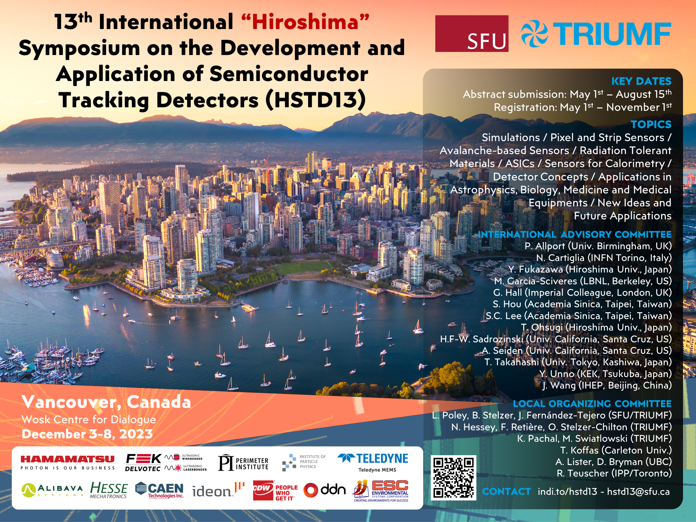
The next "Hiroshima" Symposium (HSTD13) will be held at Simon Fraser University (SFU), Vancouver, Canada, in December, 2023.

True to tradition, the primary goal of the "Hiroshima" Symposium is to bring experts in design, processing, and applications of semiconductor tracking detectors together for discussions of experiences, lessons learned, and new ideas which are still in the early stage of development.
KEY DATES:
May 1st — August 15th 31st: Submission of Abstracts
May 1st — September 30th: Early Registration (475 CAD / Student 450 CAD)
October 1st — November 1st 8th 17th: Regular Registration (550 CAD / Student 500 CAD)
Evening of December 3rd: Welcome reception
December 4th — December 8th: Symposium
February 1st 15th 2024: Deadline submission proceedings
In this study, the suppression effects of Fe on irradiation of silicon (Si) diodes were investigated. Diodes fabricated on unimplanted and Fe-implanted p-Si diodes were irradiated with 4 MeV protons to a fluence of 1x10¹⁶ p/cm-2 and then characterized prior to and after irradiation using current-voltage (I-V) techniques. A decrease in current due to irradiation is more apparent in unimplanted p-Si diode than the Fe-implanted p-Si diode, indicating that the effect of irradiation has been suppressed on the Fe-implanted p-Si diode due to Fe-doping. The diode conduction mechanism for unimplanted p-Si diode changed, while that of Fe-implanted p-Si diode remained constant after proton-irradiation. The diode parameters were also evaluated on the fabricated diodes prior to and after irradiation. The obtained results suggest that Fe-induced defects in Si have improved the radiation-hardness of Si material. Hence, Fe, just like Au and Pt, is a suitable candidate in a bid to improve the radiation-hardness of Si material.
A double arm beam telescope based on the recently developed Timepix4 ASIC was built in order to perform tests of synchronous multiple-detector readout and track reconstruction with fast timing capability. The Timepix4 is a hybrid pixel detector readout ASIC designed to record time-of-arrival (TOA) and time-over-threshold (TOT) simultaneously in each pixel. It has a 448x512 pixel matrix with square pixels at a 55μm pitch. The TOA is digitised with a 195 ps TDC bin size and the TOT is proportional to the charge collected by the silicon sensor. The telescope is composed of eight planes with n-on-p silicon sensors. Two of these planes are instrumented with 300𝜇𝑚 thick sensors tilted with respect to the beam, to provide high quality spatial measurements, while the remaining two have100 𝜇𝑚 thick sensors to achieve a better time response. Each detector assembly (sensor + Timepix4 ASIC) is cooled by a 3D printed titanium block directly attached to the test PCB, through which a cooling fluid is circulated. Both the cooling block and PCB have a circular cut-out to minimise the amount of material traversed by incident particles. The assemblies are readout by SPIDR4 systems. In addition to the Timepix4-based detectors, scintillators and a Cherenkov-MCP were placed in the beam acceptance in order to give reference timing measurements. The reference timing signals are digitised using the PicoTDC chip, that provides a fine timestamp of 3ps in its fastest configuration. First tracks were reconstructed using information from all four planes, which allows the assessment of temporal resolution using high energy particles. In this presentation, the initial results of the timing and spatial resolution of this telescope and plans for future R&D tests involving state-of-the-art sensors will be discussed.
FASER is a new experiment designed to search for new light weakly-interacting long-lived particles (LLPs) and study high-energy neutrino interactions in the very forward region of the LHC collisions at CERN. The experimental apparatus is situated 480 m downstream of the ATLAS interaction-point aligned with the beam collision axis. The FASER detector includes four identical tracker stations constructed from silicon microstrip detectors. Three of the tracker stations form a tracking spectrometer, and enable FASER to detect the decay products of LLPs decaying inside the apparatus, whereas the fourth station is used for the neutrino analysis. All tracker stations have been installed in the LHC complex in 2021. After the commissioning, FASER has been taking physics data since the start of LHC Run 3 in July 2022. In the first year of run3, we have already collected data delivered from 40 fb^{-1} (inverse femtobarns) of proton-proton collisions with a center-of-mass energy of 13.6 TeV, which allows us to achieve the first neutrino observation with a collider and constraints unexplored parameter space of dark photons. This talk describes the design, construction and performance with early data of the silicon tracker stations
The LHCb experiment has been upgraded during the second long shutdown of the Large Hadron Collider at CERN, and the new detector is currently operating at the LHC. The Vertex Locator (VELO) surrounds the interaction region of the LHCb experiment, responsible of reconstructing the proton-proton collision (primary vertices) as well as the decay vertices of long-lived particles (secondary vertices). The VELO consists of 52 modules with hybrid pixel detector technology. Compared to the previous VELO detector, the upgrade VELO encompass an enhanced track reconstruction speed and precision, even at the expected higher occupancy conditions of the upgrade, due to its pixel geometry as well as a closest distance of approach to the LHC beams, with the first sensitive pixel being at just 5.1 mm from the beam line.
Cooling is provided by evaporative CO$_2$ circulating in 500 $\mu$m thick silicon microchannel substrates. The sensors consist of 200 $\mu$m thick n-on-p planar silicon sensors, read out via 3 front-end ASICs. The detector contains 41 million 55 $\mu$m x 55 $\mu$m pixels, read out by a custom developed front-end ASIC (VeloPix). The VELO operates in an extreme environment, which poses significant challenges to its operation. During the lifetime of the detector, the sensors are foreseen to accumulate an integrated fluence of up to 8x10$^{15}$ 1MeV n$_{\rm eq}$ cm$^{-2}$, roughly equivalent to a dose of 400 MRad. Moreover, due to the geometry of the detector, the sensors will face a highly non-uniform irradiation, with fluences in the hottest regions expected to vary by a factor 400 within the same sensor. The highest occupancy ASICs foresee a maximum pixel hit rate of 900 Mhit/s and an output data rate exceeding 15 Gbit/s. The design, operation and early results evaluating the radiation damage and detector performance throughout the first year of operation will be presented.
The CMS silicon tracking system consists of an inner part with hybrid pixel modules and an outer part with silicon micro-strips. The silicon trackers have been successfully taking data during LHC Run 1 and 2. During Long shutdown 2, the pixel detector underwent an extensive refurbishment program to address the problems encountered during Run 2. The DCDC converters which exhibited failures during power cycles have been replaced. A new innermost barrel layer with improved versions of the ASICs (PROC600 and TBM) has been installed. After the re-installation of the pixel detector in June 2021 a thorough period of commissioning followed for both detectors, including the acquisition of 3.5M cosmic muon track for alignment. This contribution will summarize the refurbishment of the pixel detector during LS2 and the performance of both silicon detectors during early Run 3. The change of detector performance with increasing irradiation will be discussed including an outlook towards the end of Run 3.
The tracking performance of the ATLAS detector relies critically on its 4-layer Pixel Detector. As the closest detector component to the interaction point, this detector is subjected to a significant amount of radiation over its lifetime. At present (in 2023 LHC proton-proton collision RUN3) ATLAS Pixel Detector on innermost layers, consisting of planar and 3D pixel sensors, operate after integrating fluence of O($10^{15}$) 1 MeV n-eq cm$^{-2}$.
The ATLAS collaboration is continually evaluating the impact of radiation on the Pixel Detector. In this talk the key status and performance metrics of the ATLAS Pixel Detector are summarised, putting focus on performance and operating conditions with special emphasis to radiation damage: charge collection in data and modelling with radiation damage simulation; 3D sensors performance and comparison with planar sensors vs fluence; operational issues at high rate and mitigation techniques adopted for LHC Run3.
In June 2022 the data-taking of the Belle II experiment was stopped for the Long Shutdown 1, primarily required to install the new two-layer DEPFET detector (PXD) and upgrade components of the accelerator. In May 2023 the whole silicon tracker (VXD) was extracted from Belle II and the new VXD commissioning phase began to be ready to take data by the end of 2023. We describe the challenges and status of this upgrade. We report on the performance of the SVD in terms of the high hit efficiency and the large signal-to-noise ratio. A novel procedure to group SVD hits event-by-event, based on their time, during reconstruction allows to significantly reduce the fake rate while preserving the tracking efficiency. In the layer closest to the I.P., the SVD average occupancy has been less 0.5%, well below the estimated limit for acceptable tracking performance. Higher machine backgrounds are expected at increased luminosity and the excellent SVD hit-time information can be exploited for background rejection. We have developed a method that uses the SVD hit-time to estimate the collision time (event-T0) with similar precision to the estimate based on the drift chamber with an execution time three orders of magnitude faster. Furthermore, the front-end chip (APV25) is operated in “multi-peak” mode, reading six samples. To reduce background occupancy, trigger dead-time and data size, a 3/6-mixed acquisition mode, based on the timing precision of the trigger, has been successfully tested in physics runs.Concerning the radiation damage, the SVD dose is estimated by the correlation of the SVD occupancy with the dose measured by the diamonds of the beam-abort system. Although the moderate increase shown by sensor current and the strip noise due to radiation, we expect that the detector performance will not be seriously degraded during the lifespan of the detector.
In the HL-LHC era, the radiation is expected to reach unprecedented values, with non-ionizing fluence of 1e16 neq/cm2 and ionizing dose of 5 MGy. To cope with the resulting increase in occupancy, bandwidth, and radiation damage, the current ATLAS Inner Detector is replaced by an all-silicon system. The Pixel Detector will consist of five-barrel layers and a number of rings, resulting in about 13 m2 of instrumented area. The ITk pixel system has been very carefully designed including three different flavours of silicon hybrid detectors equipped with novel ASICS and data transmission chains. A new serial powering scheme has also been developed to minimize the amount of material in the detector. Along the lifetime of this project from design, prototyping and pre-production (current) stages many challenges have been encountered and unforeseen problems have to be solved.
At the end of this contribution the audience will get a good understanding of the status of the ATLAS-ITk pixel project and what have been the biggest challenges faced up to the day of this presentation and what are the major ones that still has to overcome.
The High Luminosity Large Hadron Collider (HL-LHC) at CERN is expected to collide protons at a centre-of-mass energy of 14 TeV and to reach the unprecedented peak instantaneous luminosity of $5-7.5x10^{34} cm^{-2}s^{-1}$ with an average number of pileup events of 140-200. This will allow the ATLAS and CMS experiments to collect integrated luminosities up to 3000-4000 fb$^{-1}$ during the project lifetime. To cope with this extreme scenario the CMS detector will be substantially upgraded before starting the HL-LHC, a plan known as CMS Phase-2 upgrade. The entire CMS silicon pixel detector will be replaced and the new detector will feature increased radiation hardness, higher granularity and capability to handle higher data rate and longer trigger latency. In this talk the Phase-2 upgrade of the CMS silicon pixel detector will be reviewed, focusing on the features of the detector layout and technological choices and summarising the R&D activities.
The High Luminosity LHC (HL-LHC) is expected to deliver an integrated luminosity of $3000-4000\;$fb$^{-1}$ by the end of 2039 with peak instantaneous luminosity reaching to about $5-7.5\times10^{34}$cm$^{-2}$s$^{-1}$. During the Long Shutdown 3 period, several components of the CMS detector will undergo major changes, called Phase-2 upgrades, to be able to operate in the challenging environment of the HL-LHC. The current silicon outer tracker has to be replaced with a new one for operating in the HL-LHC period. The Phase-2 Outer Tracker (OT) will have high radiation tolerance, higher granularity and capability to handle higher data rates. Another key feature of the OT will be to provide tracking information to the Level-1 trigger, allowing trigger rates to be kept at a sustainable level without sacrificing physics potential. For this, the OT will be made out of modules which have two closely spaced sensors read-out by a common front-end ASIC, which can correlate hits in the two sensors creating short track segments called "stubs". The stubs will be used for tracking in the L1 trigger stage. In this contribution, the design of the CMS Phase-2 OT, the technological choices and first results with pre-production devices will be reported.
Author: ATLAS-ITK Collaboration
(the speaker to be selected by the ITk Speakers Committee after the contribution acceptance)
ATLAS is currently preparing for the HL-LHC upgrade, with an all-silicon Inner Tracker (ITk) that will replace the current Inner Detector. The ITk will feature a pixel detector surrounded by a strip detector, with the strip system consisting of 4 barrel layers and 6 endcap disks. After completion of final design reviews in key areas, such as Sensors, Modules, Front-End electronics and ASICs, a large scale prototyping program has been completed in all areas successfully. We present an overview of the Strip System, and highlight the final design choices of sensors, module designs and ASICs. We will summarize results achieved during prototyping and the current status of production and pre-production on various detector components, with an emphasis on QA and QC procedures.
Many of our sensors were installed in the previous LHC, and they contributed to the discovery of the Higgs boson. This HL-LHC upgrade required significant improvements from the previous product specification, such as one-digit-higher radiation hardness, suppression of increased dark current, and a substantial increase in the number of channels . To overcome these challenges, stealth dicing technology and a high-speed inspection system were introduced during the sensor production process. As a result, we succeeded in developing a new Si photodiode array (Si strip detector, Si pixel detector) for the HL-LHC. Production and delivery started in 2020.
In addition, the following two new technologies have been established. One is the introduction of the 8-inch process line, which succeeded in increasing the size of the sensor. It has already achieved the same characteristics as the proven 6-inch line, and production started in February 2023. The other is bidding on the flip chip bonding assembly market with our pixel sensor and customer-supplied ASIC. This talk will discuss in detail our efforts in developing a new sensor for the HL-LHC upgrade.
One of the important challenges in the current radiation detector applications, as we advance in the further integration of the systems, is the cooling of the detectors. The larger heat densities, combined with the complexity of hybrid detector assemblies, complicate the full integration of the sensors, electronics, and services in the whole system. In order to overcome these difficulties micro-channel cooling has been proposed to increase the cooling efficiency, reducing the heat transfer path to the detector volume and therefore increasing the heat removal performance, while improving the integration of the cooling with the detector and front-end electronics hybrid system.
In this work, we present the development and fabrication of silicon interposers with buried micro-channels, which also incorporate a metal re-distribution layer (RDL) to contribute further in the integration of the system. These interposers are proposed for their application both in future high energy physics experiments and for advanced systems in photon science where the thermal, material, and integration requirements are very demanding, therefore they can benefit from these developments.
The microchannels and the metal tracks are created in several fabrication steps which will be described. Two methods have been followed to produce these interposers, called "pre-processing" and "post-processing", depending on whether the micro-channels are created before or after the metal lines. The advantages and disadvantages of the two approaches will be presented based on the multiple analysis techniques used to evaluate the different fabrication methods and to assess the final quality of the interposers. Additional considerations will be made on the potential of alternative technologies available to create interposers for further applications. With the advent of the Through Silicon Vias (TSV) technology, the proposed solution would provide further alternatives for the electrical interconnection of the detector/electronics hybrid with the external world, facilitating the signal and power input/output.
In high-energy physics, upgrades for particle detectors and studies on future particle detectors are largely based on silicon sensors as tracking devices. Consequently, there is a need to investigate silicon sensor concepts that offer large-area coverage and cost-efficiency.
Sensors based on the CMOS imaging technology present such an alternative silicon sensor concept for tracking detectors. As this technology is a standardised industry process it can provide a lowered sensor cost, as well as access to fast and large-scale production from a variety of vendors.
The CMOS Strips project is investigating passive CMOS strip sensors fabricated by LFoundry in a 150 nm technology. By employing the technique of stitching two different strip formats of the sensor have been realised. Besides, the strip design varies in doping concentration and width of the strip implant to study various depletion concepts and electric field configurations.
Unirradiated and irradiated samples have been characterised by probe station measurements and test beam campaigns for the different sensor designs. In addition, the detector response was simulated based on Monte Carlo methods and electric fields provided by TCAD Device simulations.
This contribution provides an overview of sensor characterisation measurements and studies on the hit detection efficiency, spatial resolution and noise of the strip sensors. The simulated detector response is presented and compared to test beam data. Furthermore, an outlook on the next sensor submission of the CMOS Strips project is given.
The Inner Detector of the ATLAS Experiment will be upgraded to a full-silicon Inner Tracker (ITk) to cope with the extreme conditions of the High-Luminosity phase of the Large Hadron Collider, currently foreseen to start with Run 4 towards 2029. In order to address the challenge of pileup in the forward region of ITk, a High Granularity Timing Detector (HGTD) will provide time track measurements with a precision of 30ps for tracks with pseudo-rapidity larger than 2.4. Due to the high radiation dose in proximity of the interaction point, the two innermost pixel layers of the ITk are designed to be replaced after 2000 $fb^{-1}$. This represents a unique opportunity to bring in technological innovation and fully exploit the potential of HL-LHC by including fast-timing through 4-dimensional (4D) tracking in the ATLAS barrel region, enabling full hermitic coverage when combined with the HGTD. In this contribution, we will demonstrate how the availability of a timestamp for the tracks in the central ATLAS region allows to significantly enhance the physics potential and discovery reach beyond what can be achieved with the HGTD alone. In order to study the impact of 4D tracking on future collider experiments, the studies are extended to a generic detector layout via the ACTS library.
In this contribution, I will describe the evolution of silicon sensors following the introduction of controlled avalanche.
We investigated the signal propagation in AC-LGAD (aka RSD), which are LGAD with a common N+ layer and AC-coupled readout contacts, by measuring the interstrip/interpad capacitances and resistances and by IR laser injection on a large selection of AC-LGAD with either strips or pads. The interest for this topic derives from the realization that while large charge sharing between strips/pads is essential for good position resolution, large sharing beyond the next two neighboring contacts generates background signals which in general are detrimental to the sensor goal of low occupancy. The observed signal is composed of the sum of the induced signal from the moving collected charge on neighboring contacts and the pick-up of the signal conducted on the N+ layer common to all contacts.
To characterize the signal propagation, we determined the interstrip/interpad capacitance and resistance using CV measurements between the contacts separated by distances of up to more than 10x the pitch values. In addition, scans of IR laser signals were added to confirm the results with charge collection.
The sensors from a variety of manufacturer had variations of the following parameters:
readout dimensions: strip/pad metal contact size (length, width), pitch,
sensor production details: N+ layer resistivity, dielectric specs (thickness, value of permittivity), bulk thickness, doping of the gain layer.
The initial data suggest that the length of the strip plays a dominant role in determining the distance the pick-up extends. On the other hand, the N+ layer resistivity influences the strength of the picked-up signal. Our study compares the effect of all parameters listed above, including comparison of different manufacturers.
Of special interest is the difference in long-distance pick-up between strip sensors and pad sensors.
The Low Gain Avalanche Detector (LGAD) is becoming increasingly a promising and important technology for soft X-ray imaging at the next generation light sources as well as for particle tracking applications in the demanding future high energy physics experiments. Different versions of LGAD have been under investigation to address specific needs for different applications. Particularly, in order to exploit the unique scientific imaging opportunities at the new XFELs, finely segmented detectors that can detect soft X-rays with energies as low as 250 eV are needed. The sensors must be able to provide an internal gain of ~10 to amplify the generated small signal to be above the noise floor of the readout electronics and must have an extremely shallow entrance window to allow the absorption of soft X-rays in the active volume of the sensor. In addition, due to the fine segmentation, the charge multiplication structure must be accommodated not on the segmented side of the sensor but on the opposite side, which would otherwise lead to extremely low fill-factors. We demonstrate a new inverse LGAD structure implemented in a sensor with n-on-n configuration as a strong candidate to fulfil these requirements. We will present the design, simulation and fabrication of the sensors as well as the preliminary characterization, including I-V and gain measurements.
Low Gain Avalanche Diodes (LGADs) represent the state-of-the-art in timing measurements and will instrument the future Timing Detectors of ATLAS and CMS for the High-Luminosity LHC. While initially conceived as a sensor for charged particles, the intrinsic gain of LGADs makes it possible to detect low-energy X-rays with good energy resolution and excellent timing (tens of picoseconds). Using the Stanford Synchrotron Radiation Lightsource (SSRL) at SLAC, several LGADs designs were characterized with energies from 5 to 70 keV. The SSRL provides 10 ps pulsed X-ray bunches separated by 2 ns intervals with an energy dispersion (ΔE/E) of 10−4. LGADs from Hamamatsu Photonics (HPK) and Brookhaven National Laboratory (BNL) with different thicknesses ranging from 20 μm to 50 μm and different gain layer designs were read out using fast amplification boards and digitized with a high bandwidth and high sampling rate oscilloscope. PiN devices from HPK and AC-LGADs from BNL were characterized as well. The feasibility of reliable Compton scattering detection with LGADs was probed. The end goal is to utilize LGADs as a pass-through beam monitoring device for high-energy X-ray beams using Compton interaction. The charge collection and multiplication mechanism were simulated using Geant4 and TCAD Sentaurus, providing an important handle for interpreting the data. In this contribution, the results of the data analysis and simulation will be shown.
The increase of the particle flux (pile-up) at the HL-LHC with instantaneous luminosities up to L ≃ 7.5 × 1034 cm−2s−1 will have a severe impact on the ATLAS detector reconstruction and trigger performance. The end-cap and forward region where the liquid Argon calorimeter has coarser granularity and the inner tracker has poorer momentum resolution will be particularly affected. A High Granularity Timing Detector (HGTD) will be installed in front of the LAr end-cap calorimeters for pile-up mitigation and luminosity measurement. The HGTD is a novel detector introduced to augment the new all-silicon Inner Tracker in the pseudo-rapidity range from 2.4 to 4.0, adding the capability to measure charged-particle trajectories in time as well as space. Two silicon-sensor double-sided layers will provide precision timing information for minimum-ionising particles with a resolution as good as 30 ps per track in order to assign each particle to the correct vertex. Readout cells have a size of 1.3 mm × 1.3 mm, leading to a highly granular detector with 3.7 million channels. Low Gain Avalanche Detectors (LGAD) technology has been chosen as it provides enough gain to reach the large signal over noise ratio needed. The requirements and overall specifications of the HGTD will be presented as well as the technical design and the project status. The R&D effort carried out to study the sensors, the readout ASIC, and the other components, supported by laboratory and test beam results, will also be presented.
Low Gain Avalanche Detectors (LGADs) are a novel silicon sensor technology being developed to design full 4D trackers able to measure precisely both spatial and temporal coordinates. The first deployment of this technology will be in the ATLAS and CMS timing layers at the High Luminosity LHC where, by adding fast timing information to each crossing track, they will allow to better separate overlapping events.
Further developments of this technology will be pursued in anticipation of their use at future collider experiments where 4D tracking detector systems will be needed to cope with an unprecedented number of pile-up and beam background events through the addition of precise timing information to each point along the track. In this context, the University of Birmingham, University of Oxford, Rutherford Appleton Laboratory and Open University are working with the UK foundry Teledyne e2v to establish their processing line for LGAD production. The addition of Te2v to the currently established LGAD manufacturers will significantly increase LGAD production volume capabilities.
This talk will present a detailed study of the performance of the first batch of LGADs produced at Te2V, before and after irradiation with 27 MeV protons. A sample of wafers with varying gain layer implant energy/dose have been tested for IV and CV characteristics, gain and timing measurements. The study is performed at different levels of fluence up to roughly 1e15 1 MeV neq/cm-2, with the goal of assessing the timing performance of these devices as a function of gain after irradiation.
The next generation of high-energy and high-intensity hadron colliders for particle physics will require tracking detectors able to efficiently record charged particles in harsh radiation environments, where expected fluences exceed 10$^{17}$ particles/cm$^2$.
Recently, thin Low-Gain Avalanche Diodes (LGADs), with an active thickness of $\sim$ 50 $\mu m$, have proven their ability to combine precise timing with precise tracking measurements, making them suited candidates for 4D tracking in future experiments. At present, the gain mechanism of LGAD sensors under irradiation is maintained up to a fluence of $\sim$ 5$\cdot$10$^{15}$ particles/cm$^2$.
To enable the usage of LGADs in the extreme fluence regime, an innovative design of the LGAD gain layer, the p$^+$ implant responsible for the local and controlled signal multiplication, has been implemented to enhance their radiation tolerance by more than one order of magnitude: the compensated LGAD.
In the standard LGAD design, the gain layer is obtained by implanting 5$\cdot$10$^{16}$ atoms/cm$^3$ of an acceptor dopant in the region below the n$^{++}$ electrode. In the compensated design, the gain layer results from the overlap of a p$^+$ and an n$^+$ implant: the difference between acceptor and donor doping will bring an effective concentration similar to standard LGADs. The new design will be more resilient to radiation, as both acceptor and donor atoms will undergo removal with irradiation, but if properly engineered, their difference will maintain constant. Therefore, the compensated LGADs will empower the 4D tracking ability to a fluence of 10$^{17}$ particles/cm$^2$ and above.
The first production of compensated LGAD sensors has been released by the FBK foundry at the end of 2022. Electrical characterisation and signal analysis from compensated LGAD sensors before and after irradiation with neutrons will be presented and discussed. Future evolution of the design of compensated LGADs will be envisaged.
Following up and finalizing the developments of former RnD projects and studies (INFN-funded TimeSPOT, Falaphel, Scaltech28 projects), The IGNITE project plans to implement an integrated system module, comprising sensor, electronics, and fast readout, specifically aimed at 4D-tracking. System pixels are required to have pitch around 50 µm and time resolution below 30 ps. In this paper we present recent advancements on the development of a prototype ASIC, designed in CMOS 28-nm technology, which explores several circuital solutions on the front-end side. The Ignite_0 development is preparatory to the design of the first IGNITE full-ASIC, featuring a 64x64 pixel matrix, being completed in the future months.
The Ignite_0 has been submitted as a mini-ASIC containing new versions of a former 4D pixel design (the Timespot1 ASIC), consisting of an Analog Front End (AFE) and a high-resolution Time-to-Digital-Converter.
The TimeSPOT-type AFE is a Charge Sensitive Amplifier with Krummenacher feedback and discrete-time Offset Compensation. Some imperfections, present in the TimeSPOT 32x32 matrix version, are here corrected. New ideas on the AFE input stage and feedback circuit, aimed at obtaining a faster response and optimizing system performance in terms of time resolution and power, are here explored as well.
The TimeSPOT TDC, based on a Vernier-type architecture, has several improvements in terms of operational and SEU robustness. Furthermore, the front-end pixel size has been changed to make it compatible with the read-out of pixels from 55 µm (TimeSPOT) to 45 µm, by modifying only a redistribution layer (upper metal) according to the specific pitch adopeted.
The Ignite_0 ASIC integrates additional important service circuits, and in particular DACs and PLLS, to test them on silicon before their integration on the 64x64 pixel matrix, which is presently ongoing.
The explored solutions will be critically illustrated during the talk, highlighting their pro and cons.
The MONOLITH H2020 ERC Advanced project aims at producing a monolithic silicon pixel ASIC with 50µm pixel pitch and picosecond-level time stamping. The two main ingredients of the project are fast and low-noise SiGe BiCMOS electronics and a novel sensor concept, the Picosecond Avalanche Detector (PicoAD). The PicoAD uses a patented multi-PN junction to engineer the electric field and produce a continuous gain layer deep in the sensor volume. The result is an ultra-fast current signal with low intrinsic jitter in a full fill factor and highly granular monolithic detector.
Testbeam measurements of the proof-of-concept PicoAD prototype, based on a 2019 ASIC design, shows full efficiency and time resolutions of 13ps at the center of the pixel and 25ps at the pixel edge, for an average of 17ps over the pixel surface.
A new monolithic prototype with improved SiGe BiCMOS electronics was produced in 2022 on a 350Ωcm substrate. Although this ASIC does not have an internal gain layer, it provided 20ps time resolution in a testbeam with pions. This prototype was irradiated with 70MeV protons with the electronics on. Laboratory measurements with a 90Sr source for a detector irradiated with 10^16 n_eq/cm^2 show a time resolution of 46ps at a sensor bias voltage of 200V, and 40 ps at 325 V.
These results give confidence that SiGe BiCMOS processes can be a candidate for the production of very high time resolution pixelated detectors for future colliders and other disciplines that involve very high radiation environments.
Future HEP experiments will consider measuring concurrently the position and the time of a particle hit with very good accuracy, i.e., 4D-trackers will be the basic option for future detection systems. Within this framework DC-coupled Resistive Silicon Detectors (DC-RSD) low-gain avalanche diodes (LGAD), an evolution of the AC-coupled design, are considered a very promising option. They combine two different design innovations, LGAD and resistive readout (RSD), to achieve a spatial resolution of a few micrometres using large pixels (150-200 micrometres), providing an excellent time resolution (~20-30 ps). The concept of DC-RSD has been finalized using an innovative mixed-mode approach to simulation: SPICE-based fast modelling to demonstrate the operating principle, followed by full 3D TCAD simulations to optimize the sensor design parameters. TCAD simulations are an excellent tool for designing this innovative class of detectors, enabling the evaluation of different technology options (e.g., the resistivity of the n+ layer, contact materials) and geometrical layouts (shape and distance of the read-out pads). In particular, a full 3D simulation domain guarantees a very accurate evaluation of the electrical behavior while providing very precise timing information, gaining access to the response of the detector device in terms of conduction and displacement currents.
This contribution reports the latest outcome of simulations, which have been instrumental in defining the design technical implementation. This contribution also describes the characteristics of the first DC-RSD production at FBK, to be submitted this summer, to explore multiple technological options and electrode layouts. Interesting information on the expected DC-RSD performance will be presented, extracted from recent experimental results obtained on AC- coupled resistive read-out sensors and on DC-RSD test structures.
Novel collider experiments demand an increased performance of the silicon detectors used, such as withstanding 1×10$^{17}$ n$_{eq}$/cm$^2$ in unprecedented pile-up conditions, and providing time resolution around 10ps. Currently, Low Gain Avalanche Diodes (LGADs) are the standard, achieving resolutions below 30ps. However, their limited radiation hardness is an area of ongoing research. As an alternative to LGADs, 3D sensors are interesting due to their proven radiation hardness. In 3D sensors, where the columns are etched into the sensor from the top (junction columns) and the back (ohmic columns), the drift distances can be very short, the depletion voltage is low and the electric field can be high, resulting in fast and short signals.
In this study, the time resolution of different 3D pixel and strip sensors was investigated with signals generated by electrons or an IR laser. Results show that 3D pixel sensors can achieve time resolutions of less than 30ps. TCT Timing measurements allow studying the position dependence of the time resolution, which is interesting for 3D sensors due to their complex electric field structure. We will show examples of position-timing maps, proving the direct correlation between time resolution and electric field. We also will demonstrate the time resolution of 3D sensors before and after irradiation, and show that 3D sensors can reach the time resolution of standard LGADs. In addition, our results demonstrate that the radiation-induced performance degradation in 3Ds can be less severe than in LGADs.
At last, we will present initial results from a production run of dedicated fast 3D sensors which have recently been produced at CNM as a common RD50 project. We will also discuss the general options for using fast 3D sensors as timing detectors in future collider experiments.
PIONEER is a next-generation experiment proposed at the Paul Scherrer Institute to perform high precision measurements of rare pion decays. By improving the precision by an order of magnitude on the charged-pion branching ratio to electrons vs. muons and the pion beta decay, PIONEER will provide a pristine test of Lepton Flavour Universality and the Cabbibo angle anomaly. At the centre of the experiment, a high-granularity active target (ATAR) will stop the pion and characterise its decay. The ATAR is being designed to provide detailed 5D tracking information, allowing the separation of the energy deposits of the pion decay products in both position and time. The chosen technology is Low Gain Avalanche Detectors (LGAD). These are thin silicon detectors with moderate internal signal amplification. Several types of LGADs still under development are being evaluated to achieve a ~100% active region, such as AC-coupled LGADs (AC-LGADs) and Trench Insulated LGADs (TI-LGADs). Since a range of deposited charge from Minimum Ionizing Particle (MIP, few 10s of KeV) from positrons to several MeV from the stopping pions/muons is expected, the detection and separation of close-by hits in such a wide dynamic range will be the main challenge. Using the CENPA Tandem accelerator at the University of Washington,we studied the LGADs response of MeV-range deposits from a proton beam. This contribution will introduce the PIONEER experiment conceptual design and its physics case. The results of the test-beam study will also be presented.
The High Luminosity upgrade of Large Hadron Collider (HL-LHC) will increase the LHC Luminosity and with it the density of particles on the detector by an order of magnitude. For protecting the inner silicon detectors of the ATLAS experiment and for monitoring the delivered luminosity, a radiation hard beam monitor has been developed. We developed a set of detectors based on polycrystalline Chemical Vapor Deposition (pCVD) diamonds and a new dedicated rad-hard front-end ASIC. Due to the large range of particle flux through the detector, flexibility is very important. To satisfy the requirements imposed by the HL-LHC, our solution is based on segmenting diamond sensors into devices of varying size and reading them out with new multichannel readout ASICs divided into two independent parts - each of them serving one of the tasks of the system. In this talk we describe the system design including detectors, electronics, mechanics and services and present preliminary results from the most recent detectors fabricated using our prototype ASIC with data from beam tests at CERN.
Irradiating a semiconductor with energetic particles gives rise to structural damage and defect formation via nonionizing energy loss processes. The build-up of stable radiation damage often proceeds via complex dynamic annealing processes, involving point-defect migration and interaction. This also occurs during the ion-implantation for electronic device fabrication and resulting defect structures depend on the density of collision cascades and the ion-beam flux. On the other hand, radiation-induced light-emitting defects, such as carbon-based defect complex of the G-center in silicon, have been regarded as promising quantum light sources for applications e.g. in quantum networking. However, the formation dynamics of these G-centers and the correlation between their optical linewidth broadening and atomic radiation disorder have rarely been studied. Here, we report on our study of the formation dynamics of G-centers in silicon for a series of proton beam flux conditions [1]. We compare the G-center optical properties characterized by time-resolved photoluminescence and observe a dose-rate effect on G center formation efficiency and optical line width. Furthermore, we perform ab initio electronic structure calculations, which provide insight into the atomic disorder induced inhomogeneous broadening by introducing vacancies, Si interstitials, and oriented strain fields in the vicinity of a G center. Our results can guide directions for the efficient formation of G centers for quantum applications. Moreover, our results indicate that the optical signal from G-centers enables atomic scale sensing and characterization of radiation damage resulting from ultradilute low-fluence irradiation, e.g., expanding capabilities for dark-matter searches.
References:
[1] W. Liu, et al., “Quantum Emitter Formation Dynamics and Probing of Radiation-Induced Atomic Disorder in Silicon”, Phys. Rev. Appl. 20, 014058 (2023)
Acknowledgment
This work at Berkeley Lab was supported by the Office of Science, Office of Fusion Energy Sciences, and Office of High Energy Physics, of the U.S. Department of Energy, under Contract No. DE-AC02-05CH11231.
The proven radiation hardness of silicon 3D devices up to fluences of $1 \times 10^{17}\,n_{eq}/cm^{2}$ makes them an excellent choice for next generation trackers, providing $<10\,\mu m$ position resolution at a high multiplicity environment. The anticipated pile-up increase at HL-LHC conditions and beyond, requires the addition of < 50 ps per hit timing information to successfully resolve displaced and primary vertices. In this study, the timing performance, uniformity, and efficiency of neutron and proton irradiated single pixel 3D devices is investigated. Three different geometrical implementations are evaluated for fluences up to $1\times10^{17}\,n_{eq}/cm^{2}$ at 120 GeV SPS pion beams. The question of electronic bandwidth is also addressed, with respect to achievable time resolution, efficiency and collected charge. In such a tri-dimensional phase-space, an appropriate operating point is selected depending on the application requirements. A MIMOSA26 type telescope is used to provide detailed tracking information with a ~$ 5\,\mu m$ position resolution. Productions with single- and double-sided processes, yielding active thickness of 130 and 230 $\mu m$ respectively, are studied, with pixel sizes that vary from $55 \times 55\,\mu m^{2}$ to $25 \times 100\,\mu m^{2}$. A comparison of field uniformity with respect to electrode geometry is presented, as well as a time resolution study for incidence angles up to 12$^{\circ}$.
With the upgrade of the LHC to the High-Luminosity LHC (HL-LHC), the Inner Detector will be replaced with the new all-silicon ATLAS Inner Tracker (ITk) to maintain tracking performance in a high-occupancy environment and to cope with the increase in the integrated radiation dose.
Comprising an active area of 165m2, the outer four layers in the barrel and six disks in the endcap region will host strip modules, built with single-sided micro-strip sensors and glued-on hybrids carrying the front-end electronics necessary for readout. Before being shipped out for module building, the ATLAS18 main sensors were tested at different institutes in the collaboration for mechanical and electrical compliance with technical specifications, the quality control (QC), while fabrication parameters were verified on test structures from the same wafers, the quality assurance (QA).
As part of ongoing studies in parallel to ITk Sensor Production QC and QA, diodes fabricated as part of the test structures were measured using Deep-Level Transient Spectroscopy (DLTS). This was done to achieve precise sensor simulations motivated by findings of anomalous leakage current behaviour, as well as to compile a more complete model of radiation damage in ITk Strip Sensors. Utilising DLTS spectra with varying test parameters, trap energy levels and cross-sections associated with defects in the devices were obtained. Furthermore, employing related measurements techniques, such as Thermal Admittance Spectroscopy (TAS), results were supplemented and expanded, or additional points of interest, such as the deep level profile and the capture kinematics of the trap levels, were investigated with double-pulse DLTS (DDLTS).
In this talk, results of the defect characterisation will be given. Spectra for unirradiated and irradiated diode samples from both prototyping and production period will be presented, and their details collected from Arrhenius analyses will be shown.
The production of strip sensors for the ATLAS Inner Tracker (ITk) started in 2021. During this time, a Quality Assurance (QA) program is being carried out continuously, by using specific test structures, in parallel to the Quality Control (QC) inspection of the sensors. The QA program consists of monitoring sensor-specific characteristics and the technological wafer process variability, as produced and after the irradiation with gammas, neutrons, and protons. After two years, half of the full production volume has been delivered and we present statistical and time-evolution information of the parameters measured as part of the QA performance.
The main devices used for QA purposes are miniature strip sensors, monitor diodes and the ATLAS test chip, which contains several test structures (e.g., bias resistors, interdigitated structures or field oxide capacitors). Such devices are tested by several sites across the collaboration depending on the type of samples (non-irradiated components or irradiated with protons, neutrons, or gammas).
All the parameters extracted from the tests are uploaded to a database, from which they are selected in the analysis process by the use of newly developed python scripts which interrogate the database, filter the data, and perform analysis, statistics and representation. These parameters are summarized in the form of histograms, time-evolution plots and correlation plots to get parameter distributions, trends, and meaningful parameter-to-parameter correlations. The purpose is to identify possible deviations in the fabrication, the sensor quality, or alternatively, changes in the behaviour of the test equipment or possible variability in the irradiation processes.
The results from these two years of production of the strip sensors of the ITk are presented. They have allowed the optimization of the measurements, setting soft limits, and analysis, and a better understanding of the device properties and fabrication trends. Those abnormal results are fed back to the vendor promptly.
The new all-silicon Inner Tracker (ITk) is being constructed by the ATLAS collaboration to track charged particles produced at the High-Luminosity LHC. The outer portion of the ITk detector will include nearly 18,000 highly segmented and radiation hard silicon strip sensors (ATLAS18 design). Throughout the production of 22,000 sensors, anticipating expected losses, the strip sensors are subjected to a comprehensive suite of mechanical and electrical tests as part of the Quality Control (QC) program. In a large fraction of the batches delivered to date, high surface electrostatic charge of 80 to several 100s of volts was measured. High static charge was also measured on the plastic sheets which sheathe the sensors for shipping and handling rigidity. Aggregate data from across QC sites indicate a correlation between observed electrical failures and the sensor/plastic sheet charge build up. To mitigate these issues, the QC testing sites introduced recovery techniques involving irradiation of the sensor surface with UV light or application of intensive flows of ionizing gas to remove accumulated static charge. In addition, significant modifications to sensor handling procedures were made to prevent subsequent build up of static charge. This presentation details a precise description of the issue, trend analyses of sensors initially failing electrical tests (I-V, strip scan, etc.) and their performance over time after the recovery treatment. We also discuss results after mitigation attempts by the vendor, and interesting cases where little static charge was observed.
The new ATLAS Inner Tracker (ITk) will replace the current tracking detector of the ATLAS detector to cope with the challenging conditions for the Phase-II upgrade of the Large Hadron Collider experiment (LHC), the so-called High Luminosity LHC (HL-LHC). The new tracking detector is an all-silicon detector consisting of a pixel inner tracker and a silicon microstrips outer tracker, differentiated again in a central barrel section around the interaction point and two end-cap sections covering the forward regions for the collisions.
This contribution focuses on the currently developed full system tests for the ITk strips detector, being the testbed for testing and evaluating the performance of several close-to-final detector components before production. These will also serve in the future for training and testing purposes of the detector during operation.
The barrel system test is conducted in SR1 at CERN and will consist of 8 staves - mechanical core structures loaded with rectangular short (~ 2.5 cm) and long (~5 cm) strip sensor modules. In a similar fashion, the system test for the end-caps is developed at DESY in Hamburg/Germany loaded with up to 12 petals - again a core structure loaded with trapezoidal shaped sensors of various lengths and strip pitches including the readout and power electronics. The staves and petals are mechanically held in place within a support structure and connected to the electrical, optical and cooling services as realistic as possible as in the latter detector integration. As such it is possible to validate the detector design, verify the detector DAQ and perform tests with the services, e.g. concerning the dual-phase CO${}_2$ cooling.
This contribution gives an overview of the developed system tests for the ITk strip detector, summarizes the current status of the two sites, and shows a selection of performance measurements conducted in the last months.
In preparation for the forthcoming High-Luminosity phase of the Large Hadron Collider, the ATLAS experiment is working on major upgrades to its detector systems to effectively accommodate the increase in radiation levels and track density. The foremost among these upgrades entails the replacement of the current inner tracking detector with an advanced all-silicon Inner Tracker (ITk). In the outer region of the ITk apparatus is the Strip Detector.
Central to the new strip tracking system are the ITk Strip modules, comprising silicon sensors and hybrid Printed Circuit Boards housing the integral read-out Application-Specific Integrated Circuits (ASICs) as well as power distribution services. Thorough characterization of the electrical characteristics of the silicon strip modules at various stages of the assembly procedure holds paramount significance in evaluating module performance. This rigorous evaluation ensures timely identification of any anomalies, thereby enabling proactive remedial measures. Notably, during the course of these electrical assessments, certain modules manifested breakdown phenomena occurring below the prescribed threshold of 500 V, as mandated by the ITk Quality Control protocols.
Based on these observations, controlled exposure to low levels of radiation was suspected to elevate the breakdown voltage in susceptible sensors. This contribution presents results from two irradiation campaigns to investigate potentially beneficial effects of irradiation. One study investigates the effects of gamma irradiation on complete modules showing an early breakdown due to glue spreading over the sensor guard ring. For this study, modules were exposed to an ionizing dose of 11 krad (corresponding to the dose accumulated after several days of operation in the HL-LHC) utilizing a 60Co source. The second campaign focuses on silicon sensor test structures with low breakdown voltage due to intentionally caused mechanical defects and their development after exposure to reactor neutrons. In both cases, preliminary findings suggest a discernible improvement in the breakdown voltage.
The ATLAS experiment at CERN will replace its tracker with an all-silicon tracker during the Phase II upgrade for the High Luminosity LHC. The tracker is comprised of a pixel-based detector at lower radius and a strip-based detector at higher radius. The application specific integrated circuits (ASICs) for the strip tracker are nearing the end of their production. The analog front-end ASIC for the strip detector is the ABCStar. The ABCStar consists of the analog front-end, the first level trigger latency buffer and event buffer and digital readout circuitry. The production process will be discussed as well as a significant issue that was discovered during production and the mitigations applied.
The Belle II experiment at the SuperKEKB collider in Tsukuba, Japan, has collected $e^{+}e^{-}$ collision data between 2019 and 2022. After reaching a record-breaking instantaneous luminosity of $4.7 \times10^{34} ~\text{cm}^{-2}\text{s}^{-1}$ and recording a dataset corresponding to $424 ~\text{fb}^{-1}$, it is currently in its first planned long shutdown phase (LS1) until December 2023. Aside from upgrades of the collider and detector maintenance, the shutdown is used for the installation of the two-layer Pixel Vertex Detector (PXD) which forms the Belle II Vertex Detector (VXD) together with four layers of double-sided silicon strips (SVD). The VXD is essential for precisely reconstructing primary and decay vertices. As the innermost sub-detector, multiple scattering effects need to be reduced. PXD utilizes the depleted P-channel Field Effect Transistor (DEPFET) technology, allowing for a $75 ~\text{$\mu$m}$-thin sensitive detector area and a low material budget of $0.21~\%$ $X_{0}$ per layer. Each of the tracker's 40 modules consists of an array of $256 \times 768$ pixels with a pitch ranging from $(50 \times 55) ~\mu \text{m}^{2}$ for the inner to $(85 \times 55) ~\mu \text{m}^{2}$ for the outer layer yielding high gain and high signal-to-noise ratio while retaining about $99 ~\%$ hit efficiency. This talk will discuss the experience of the 4-year operation
of the previous single-layer PXD in harsh background conditions as well as commissioning and testing of the fully-populated PXD2 during LS1.
Test Beam characterisation is the gold standard test to prove novel detector concepts based on precisely reconstructed and time-tagged particle trajectories. This is done by beam-telescopes that are expected to have high spatial and good temporal resolution. Telescopes data needs to be synchronised with various readout types: Triggered readout architectures, data-driven approaches and devices with fixed shutter intervals. This flexibility is realised with a trigger logic unit (TLU) providing a common clock, trigger and trigger IDs. Steering of the TLU and beam telescopes can be provided in the EUDAQ2 DAQ framework. Upgrades of the telescope are currently being developed based on the successful existing systems, to cope with increasing rate and precision requirements. An additional region of interest triggers with a time resolution of a few nanoseconds and LGADS as high precision timing layers with a resolution below 100ps are being commissioned.
To reconstruct the data recorded at test beams, the Corryvreckan framework has been developed and is provided to users. It is an open source project, allowing for flexible event building supporting all kinds of readout modes of new prototypes. It can natively read in data recorded with EUDAQ2 and hence telescope and TLU data from the DESY II test beams. Additionally Corryvreckan features modules for clustering in space and time, basic correlations, track reconstruction, detector alignment and device under test efficiency study.
The contributions aims to introduce the current status and upgrade projects of the DESY infrastructure to motivate the need for flexible reconstruction frameworks. Afterwards the Corryvreckan framework will be presented with an emphasis on the event building, track reconstruction and alignment capabilities. Finally selected characterisation results of timing layer upgrades for the telescopes are presented to showcase the capabilities of Corryvreckan and an outlook towards future improvements of the facilities and software framework will be given.
Monolithic Active Pixel sensors (MAPS) have been undergoing significant advances over the last decade in terms of integration densities, radiation hardness and speed. They became the technology of choice for precise vertex detectors at high energy physics experiments with moderate radiation loads, notably STAR at RHIC, ALICE at LHC, and are being considered for future FCC-ee detectors.
Being based on commercial CMOS imaging processes, MAPS naturally benefit from the fast progress in the field of commercial imaging. In particular, smaller feature sizes and larger wafers are becoming available now; 65 nm on 300 mm wafers are the state of the art today. Typical sensitive layer thickness are 30 μm or even less, depending on the technology, allowing overall thickness of only 50 μm. At those thicknesses, the sensors become flexible enough to be bent into truly cylindrical shapes down to radii below 2cm. Together with a processing option called stitching, it is possible to produce sensors of wafer scale, making it possible to build real detector half-cylinders out of single sensors, which brings down the material budget to a minimum.
This contribution will showcase the state of the art of wafer-scale, bent MAPS, detail the design challenges, report on first results from prototype circuits, and outline the next steps to make technology available for the first applications. In particular, a number of recent results from a first prototype run with two different 26 cm long MAPS will be given.
The new Inner Tracking System (ITS2) of the ALICE experiment at the LHC, upgraded during the LHC Long Shutdown 2 (2019-2021) with CMOS monolithic active pixel sensors (ALPIDE), is currently taking data and demonstrating excellent performance in the LHC Run 3. A replacement of the three innermost layers of the ITS2, called ITS3, is foreseen during the LHC Long Shutdown 3 (2026-2028) in order to further improve tracking precision and efficiency, particularly at very low transverse momentum (pT > 0.1 GeV/c).
The ALICE ITS3 is a cylindrically bent silicon vertex detector based on stitched wafer-scale monolithic active pixel sensors with a 65 nm CMOS technology. The large stitched sensors are 28 cm in length and can be thinned down to below 50 µm, where the sensors are flexible to be bent to form truly cylindrical half-barrels. Air-cooling is feasible thanks to the reduced sensor power consumption of < 20 mW/cm2. An extremely low material budget of 0.05% X/X0 can be achieved in combination with lightweight carbon foam spacers as support structures.
This new technology for ITS3 was qualified with a set of test structures from the first submission (called MLR1: Multi-Layer Reticle 1). A successor prototype with dimensions of 14 x 259 mm, called MOnolithic Stitched Sensor (MOSS), has been designed to demonstrate the feasibility of the stitching process. Comprehensive laboratory characterizations and beam tests are underway to study the performance of MOSS.
In this contribution, the ALICE ITS3 detector concept, sensor bending mechanics and technology qualification achieved through MLR1 prototypes will be concisely reviewed. The MOSS design and its test system will be introduced, and the first results of the MOSS characterization in terms of manufacturing yield, power distribution and efficiency, data rates, noise, charge threshold, detection efficiency and spatial resolution will be discussed in detail.
Recently, more than 300 satellites are launched globally every year, significantly lowering the hurdle to space exploration. Particularly, small satellites weighing less than several tens of kilograms are widely used in industry and telecommunications, but they are also crucial as a pathfinder for cutting-edge space science. Tokyo Tech successfully launched the 50 kg university satellite HIBARI in 2021, and plans to launch a second satellite, PETREL, in the second half of FY 2023. Both satellites attempt to control the attitude by variable geometry in orbit, and to observe ultraviolet radiation in the very early phase of the gravitational wave objects like kilonova (neutron star–neutron star merger). In this talk, I will first review these university satellite projects and then report on the world's first MeV gamma ray small observation satellite (tentative name: INSPIRE), which is scheduled to be launched in FY2026. The satellite carries a Compton-camera box (CC-BOX), which can visualize 30–3000 keV X-/gamma-rays, along with high-sensitivity UV camera. CC-BOX consists of large area Si-PM (MPPC) array optically coupled with 3D position-sensitive Ce:GAGG scintillator to achieve an angular resolution of 7° (FWHM) by simultaneous imaging of 30–200 keV in pinhole mode and 200–3000 keV in Compton mode. The field of view is ~1 str in every pointing. The prototype model of CC-BOX has already been installed and tested for diagnostic imaging in nuclear medicine and observation of atmospheric phenomena, such as in the world's first successful gamma ray imaging of thunderclouds (Kuriyama et al. 2022, GRL). In this talk, I will describe in detail the imaging experiments using the prototype model to date, along with various environmental tests for the launch in FY2026. I will also discuss expected performance and observation plans in orbit to achieve various scientific goals.
The monolithic X-ray SOI-CMOS detector "XRPIX" integrates a sensor layer and a CMOS layer by sandwiching an insulating layer made of SiO2 using SOI technology. This detector is planned to be installed in future X-ray satellites. SOI technology allows us to implement complex CMOS readout circuits. The detection efficiency is high even for X-rays above 10 keV due to the thick depletion layer of several hundred μm. Therefore, by implementing the self-trigger function in pixel circuits, the time resolution of XRPIX is less than 10 μs, which is excellent for observing time-varying celestial objects. In order to achieve a large imaging area in the limited space of the satellite, it is essential that the ADC (analog-to-digital converter) be mounted on the detector (on-chip).
We developed XRPIX9 with on-chip ADC and evaluated the performance of the ADC. The XRPIX9 is equipped with 16 units of 14-bit cyclic ADCs to read out 8 columns. And their convert speed is 5.96 μs. Cyclic ADC performs binary search by repeatedly using a common amplifier and comparator for the number of bits, thus enabling high-precision AD conversion in a small footprint. To evaluate the cyclic ADC, at first, external signals were input to the ADCs by connecting with the function generator. We evaluated the integral nonlinearity, differential nonlinearity, and input noise of the ADC, which were found to be 0.06%, 0.5 LSB, and 3 LSB respectively. We also irradiated XRPIX9 with 5.9 keV X-rays from 55Fe, then we successfully obtained X-ray signals via on-chip ADC. In this presentation, we will report these evaluations of the performance of on-chip ADC and their details.
Cosmic MeV gamma-ray observations are important for understanding physics in high-energy astronomical objects such as gamma-ray bursts and blazars. However, there has been no progress since COMPTEL on board the Compton Gamma Ray Observatory in the 1990s, thus a new satellite for MeV gamma-ray observations is needed. Compton scattering is the dominant interaction between MeV gamma-rays and matter. The minimal way to reconstruct the arrival direction of an incident gamma-ray is to utilize both the deposit energy and hit position measured in both the scatterer and absorber, giving an event circle. In order to improve the angular resolution, one can measure the track of the Compton-scattered electron with a pixel sensor and utilize the estimated initial momentum of the electron to reduce the circle to an arc. We have been evaluating an event-driven Silicon-on-Insulator (SOI) pixel detector XRPIX8.5 as a scatterer for future MeV gamma-ray telescopes. XRPIX is a detector that incorporates both a thick depletion layer and high-speed, low-noise CMOS pixel circuits simultaneously by utilizing SOI technology and issues trigger and coordinate information immediately after detecting signal. The pixel size of XRPIX8.5 is 36 um square and thus it is expected to measure electron tracks for gamma rays with the energy of several hundred keV since, for instance, an electron with the energy of 300 keV creates a track of ~500 um in silicon. In this contribution, we report on the evaluation of the depletion layer thickness of XRPIX8.5, which can be fully depleted at room temperature, the sensor response when irradiated with gamma-rays such as 662 keV of Cs-137 and 511 keV of Na-22, and a method for estimating the initial direction of electron track.
We have been developing the high-voltage CMOS active pixel sensor, AstroPix, mainly for the future gamma-ray space telescope, AMEGO-X. The gamma-ray detector of AMEGO-X consists of four identical stacked silicon tracker towers and requires $\sim6\times10^4~\rm{cm^2}$ silicon area. The scientific purpose of the AMEGO-X mission dictates a number of requirements on the performances of the instrument, such as the energy range (25 keV - 1 GeV) and resolution, which affects the design of the detector. AstroPix has to be $500~\rm{\mu m}$ thick and to be fully depleted by supplying bias voltage. Also the energy resolution must be $<10\%$ (FWHM) at 60 keV and the pixel pitch should be $500\times500~\rm{{\mu m}^2}$ in order to achieve the desired angular resolution of the gamma-ray detector. Furthermore, given the space-based nature of AMEGO-X, the power consumption of AstroPix needs to be limited ($<1~\rm{mW/{cm}^2}$). The first version of AstroPix was developed based on the experience of the developments of both ATLASPix and MuPix. Our development strategy is to incrementally upgrade the chip design towards fulfilling the requirements for AMEGO-X. While the development is under way, the latest version of AstroPix already reached the target pixel pitch. In this contribution, we report about the AstroPix developments and performance, such as I-V, noise, energy calibration/resolution/threshold, depletion depth, and their radiation tolerance.
Monolithic active pixel sensors (MAPS) produced in a 65 nm CMOS imaging technology are being investigated for applications in particle physics. Their main characteristic is integrating a sensing volume and readout circuit in the same silicon wafer, reducing material budget with respect to most hybrid sensors. Compared to the previously investigated 180 nm CMOS imaging technology, the 65 nm technology significantly improves the logic density of the circuitry. The investigated sensor design has a small collection electrode characterized by a low input capacitance, granting a high signal-to-noise ratio and low power consumption. These features are the main motivation for the Tangerine project, which aims to develop the next generation of silicon pixel sensors with a temporal and spatial resolution compatible with the requirements for a vertex detector at future lepton colliders. The developments are pursued in collaboration with the CERN EP R&D program on technologies for future experiments and with the ALICE ITS3 upgrade.
The project comprises all aspects of sensor development, from electronics engineering and sensor design using simulations, to laboratory and test-beam investigations of prototypes developed within Tangerine and the collaborating projects. The use of simulations when developing a MAPS is of great relevance, given the complex electric field configuration and the simultaneous need for high statistics. TCAD device simulations using generic doping profiles and Monte Carlo simulations have been used to build an understanding of the technology and predict the performance parameters of the sensor. Prototypes of a 65 nm CMOS sensor with a small collection electrode have been characterized in laboratory and test-beam facilities by studying their charge collection, spatial resolution, and efficiency. This contribution compares simulation results to test-beam data. The experimental results validate the employed simulation approach and establish this technology as a promising candidate for a vertex detector at future lepton colliders.
The proposed Circular Electron Positron Collider (CEPC) presents new challenges for the vertex detector in terms of material budget, spatial resolution, readout speed, and power consumption. To address these challenges, a Monolithic Active Pixel Sensor (MAPS) prototype called TaichuPix has been implemented, which is based on a column drain readout architecture. The TaichuPix sensor chip has been characterized at the DESY test beam facility, and the results indicate a spatial resolution better than 5 µm and a detection efficiency better than 98% under the set threshold.
The baseline vertex detector is proposed with a three-ladder architecture, which will be double-sided with TaichuPix sensors. The double-sided structure is adopted to reduce the multiple scattering of particles and improve the impact parameter. This means that the silicon pixel sensors and cables are installed on both sides of the support structure. A ladder is made of common support together with two layers of silicon detectors. For this prototype, one side of a ladder is proposed to assemble two TaichuPix sensors on a flexible printed circuit board. Two flexible boards are installed on the front and back sides of the lightweight carbon fiber support structure.
To verify the performance of the baseline vertex detector, six ladders were installed on the barrel, and the beam test was conducted at the DESY II TB21 facility. The beamline runs straight through the prototype, producing precise reconstruction points by multi-layer TaichuPix sensors. This presentation proposes to show the architecture and beam test results of the baseline vertex detector prototype.
Detectors based on Chemical Vapor Deposition (CVD) diamond have been used successfully in beam conditions monitors in the highest radiation areas of the LHC. Future experiments at CERN will accumulate an order of magnitude larger fluence. As a result, an enormous effort is underway to identify detector materials that can operate after fluences of 10^{16}/cm^2 and 10^{17}/cm^2. Diamond is one candidate due to its large displacement energy which enhances its radiation tolerance.
Over the last few years the RD42 collaboration has constructed and characterized detectors using CVD diamond material with a planar geometry and more recently with a 3D geometry to extend the materials' radiation tolerance. In this talk, we present test beam results of the latest planar and 3D diamond pixel detectors measured in the MALTA telescope at CERN using our prototype diamond detector ASIC. The 3D cells in these detectors have a size of 50µm x 50µm with columns 2.6µm in diameter and 100µm x 150µm with columns 4.0µm in diameter. A description of the production techniques used to produce these devices and beam test results for detectors will be presented and compared.
Monolithic active pixel sensors featuring depleted substrates (DMAPS) present a promising alternative for pixel tracker detectors operating in high-radiation and high-rate environments. The utilization of higly resistiv silicon substrates and high-voltage capabilities within commercial CMOS technologies holds the potential to significantly enhance radiation tolerance with respect to MAPS. TJ-Monopix2 and LF-Monopix2 chips are the most recent large-scale prototype chips in their respective development lines with a column-drain readout architecture.
Designed in 150 nm LFoundry technology, LF-Monopix2 uses a large charge collection electrode with pixel electronics embedded in it. Benefits of this design are short drift paths and a homogeneous electric field across the sensor that increase the radiation tolerance. Optimization of the pixel layout minimizes potential coupling from the digital circuitry into the sensor node while reducing the pixel size to 50 x 150 um² compared to its predecessor.
TJ-Monopix2 is designed in 180 nm Tower Semiconductor technology. Featuring a small charge collection electrode design with separate readout electronics, the pixel pitch of this sensor could be reduced to 33 x 33 um². A small detector capacitance allows for a large signal-to-noise ratio while an additional n-type layer across the pixel ensures full depletion of the sensitive volume.
In this talk, the latest test beam results of both DMAPS are presented. Timing studies and charge collection measurements of TJ-Monopix2 are highlighted. Performance of irradiated LF-Monopix2 chips after a fluence of up to 2e15 neq/cm² is shown.
The Super-KEKB collider is set to undergo a major upgrade to achieve a target luminosity of
$6*10^{35}cm^{-2}s^{-1}$. A long shutdown is foreseen around year 2027, which provides the
opportunity to revisit parts of the Belle II experiment.
A new pixelated vertex detector (VTX) is being developed to match the upgraded interaction region.
This silicon tracker aims to be more robust against the expected higher machine background and improve
precision and standalone track finding efficiency.
The proposed VTX design comprises of five layers in a barrel-shaped configuration with minimal material budget.
The innermost layers are based on an "all-silicon ladder" concept with air cooling, targeting a material budget below 0.2% X0/layer.
For the three outer layers, liquid cooling and carbon-fiber support structures based on on ALICE-ITS2 with
a material budget ranging from 0.3% X0 for later 3 up to 0.8% X0 for layer 5 will be used.
All the ladders feature the OBELIX depleted-MAPS CMOS sensor, with an active area of approximately 2 cm × 3 cm, designed in the Tower 180 nm technology.
The pixel-matrix, derived from the TJ-Monopix2 sensor developed for the ATLAS experiment, has a 33 μm pitch an integration time of less than 100 ns.
The power-dissipation is less than 200$mW/cm^2$ at an average hit-rate of 60 $MHz/cm^2$. A digital trigger logic is designed to meet Belle II requirements,
targeting a 30 kHz average trigger-rate with a 10 μs trigger delay and a maximum hit-rate of 120 $MHz/cm^2$.
The initial version of the sensor is expected to be designed and submitted for foundry production by late 2023.
The presentation will encompass various aspects of the project, including tests of the TJ-Monopix2 to validate pixel-matrix performance,
a detailed focus on the OBELIX features and design status as well as prototype fabrication and testing of the mechanical concepts.
MALTA2 is a depleted monolithic active pixel sensor developed in the Tower Semiconductor 180 nm CMOS imaging process. Monolithic CMOS sensors offer advantages over current hybrid imaging sensors both in terms of increased tracking performance due to lower material budget but also in terms of ease of integration and construction costs due to the integration of read-out and active sensor into one ASIC. Current research and development efforts are aimed towards radiation hard designs up to 100 Mrad in Total Ionizing Dose and $3\times10^{15}$ $1$ $MeV $ $n_{eq}/cm^2$ $ $ in Non-Ionizing Energy Loss . One important property of a sensor's radiation hardness is the depletion depth at which efficient charge collection is made via drift movement. Grazing angle test beam data was taken during the 2023 SPS CERN Test Beam with the MALTA telescope and Edge Transient Current Technique studies were performed at DESY in order to develop a quantitative study of the depletion depth for both un-irradiated and irradiated MALTA2 samples. These measurements together with efficiency, cluster size and timing measurements before and after neutron irradiation show that MALTA2 is an interesting tracking sensor for HL-LHC and beyond collider experiments, providing both very good tracking capabilities and radiation hardness in harsh radiation environments.
Silicon Photomultipliers (SiPMs) are state-of-the-art photon detectors used in particle
physics, medical imaging, and beyond. They are sensitive to even single photons in the
optical wavelength regime and achieve time resolutions in the order of 10 ps, which makes
them candidates for timing detectors in tracking systems. The Geiger-discharge triggered
in the sensitive elements of a SiPM, Single-Photon Avalanche Diodes (SPADs), yields
signal amplitudes independent of the energy deposited by a photon or ionizing particle.
This intrinsically digital nature of the signal motivates its digitization already on a SPAD
level.
A digital SiPM (dSiPM) developed at Deutsches Elektronen Synchrotron (DESY), and
produced in a LFoundries 150-nm CMOS technology is presented, introducing embedded
CMOS circuitry for on-chip signal processing. Key features of the DESY dSiPM are
hit position information on a pixel level, and hit time stamps per quadrant and 3 MHz
readout frame. The pixels comprise four SPADs and have a pitch of 70 μm. The four
time stamps are provided by 12 bit Time-to-Digital Converters (TDCs) with a resolution
below 100 ps.
The chip is investigated in the laboratory to determine dark count rate, breakdown
voltage, and TDC characteristics. Test-beam measurements demonstrate synchronous
integration in a detector system, spatial hit resolution on a pixel level, and are used to
study minimum-ionizing particle detection efficiency and time resolution.
The Single Photon Avalanche Diode (SPAD) technology relies on saturated gain, i.e. the complete discharge of the diode, for detecting single charge carriers, electrons or holes, usually produced by single photons. SPADs will detect the carriers produced by charged particles, however the signal may be buried in thermal noise, without the ability to identify one (thermal) carrier from multiple ionization carriers. We introduce the ASGAD concept that overcome this issue, and enable high purity detection of charge particles enabling to achieve the outstanding timing resolution of SPADs, that is expected to be 10ps or better for digital SPADs. In general we will discuss the pros and cons of using saturated gain avalanche diodes associated with integrated digital electronics for tracking. We will also look at how this technology can be used beyond single photon detection for dark matter search and keV scale electron detection.
We propose a novel APD array showing near 100% fill factor. The APDs operate in proportional mode at low or moderate gain and exhibit very high detection efficiency also in inter pixel gap regions. By applying a fully depleted reach-through structure light entrance side and electronics side are kept separated. In contrast to common APD arrays the avalanche process is sustained in the inter pixel gap regions as well. A non structured boron doped multiplication region (MR) extends over the entire array. Parasitic early breakdown at the n+ pixel edges is caused by electric field peaks near to convex doping shapes. In our approach it is suppressed by a n-doped layer, called field drop region (FDR), located directly beneath the n+ pixels. The positive space charge of this fully depleted layer causes a reduction of the electric field to a non-critical level when it reachs the n+ edges. The FDR gets depleted by the negative MR space charge preventing pixel shortage. We started a first prototyping on 450µm thick p-type float zone. Measures for excess noise reduction are implemented to optimize the sensor for photon science applications. For MR a high energy implantation was chosen. The peak concentration is in a depth of about 6µm. Due to the wider MR a lower electric field is required to achieve the same gain. Lower electric field results in a smaller k value (hole/electron ionization rate) and lower excess noise. Since MR and FDR implantations are lithographically confined to the area of the APD array a classical multi guard rings can be used for edge termination. The prototype design contains small pixel and strip arrays for eta-plot measurements. We will present a detailed description of the operating principles and plan to compare first measurements with simulations.