20th Real Time Conference

Europe/Rome
Padova, Italy

Padova, Italy

<a href="https://goo.gl/maps/vWFxL">Centro Congressi A. Luciani Via Forcellini, 170/A Padova ITALY</a>
Adriano Luchetta (Consorzio RFX), Dora Merelli (IEEE), Gianluca Moro, Martin Grossmann, Martin Lothar Purschke (Brookhaven National Laboratory (US)), Patrick Le Dû, Rejean Fontaine (Université de Sherbrooke), Sascha Schmeling (CERN), Stefan Ritt (Paul Scherrer Institute), Zhen-An Liu (IHEP,Chinese Academy of Sciences (CN))
Description

20th Real Time Conference

Welcome to Padova!

Photo of RT2016 participants at Palazzo del Bo . UNIPD - 6 June 2016 - low resolution2016


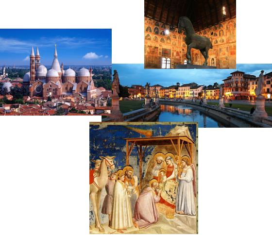
We invite you at the Centro Congressi “A. Luciani” in Padova for the 2016 Real Time Conference (RT2016). It will take place Monday 6 through Friday 10 June 2016, with optional pre-conference tutorials Sunday, June 5.

Like the previous editions, RT2016 will be a multidisciplinary conference devoted to the latest developments on realtime techniques in the fields of Plasma and Nuclear Fusion, particle physics, nuclear physics and astrophysics, space science, accelerators, medical physics, nuclear power instrumentation and other radiation instrumentation.


Padova


Important Dates:

  • June 5, 2016 - Short-Courses
  • June 6-10, 2016 -  Conference 


Sponsors


Registration
Exhibitor Form
Exhibitors accompanying
Surveys
Bus Transportation to/from Conference Venue
    • Short Course - Real-time data visualization and control using modern Web technologies Caffe Pedrocchi (Padova)

      Caffe Pedrocchi

      Padova

      • 1
        Real-time data visualization and control using modern Web technologies 1 Caffe Pedrocchi (Padova, Italy)

        Caffe Pedrocchi

        Padova, Italy

        Via VIII Febbraio, 15 35122 Padova (PD)
        Speaker: Stefan Ritt (Paul Scherrer Institute)
      • 11:00
        Coffee Break Caffe Pedrocchi (Padova)

        Caffe Pedrocchi

        Padova

      • 2
        Real-time data visualization and control using modern Web technologies 2 Cafe Pedrocchi, Padova

        Cafe Pedrocchi, Padova

    • 09:35
      Registration Caffe Pedrocchi (Padova)

      Caffe Pedrocchi

      Padova

    • Break: Lunch
    • Short Course - Real-time data acquisition and processing applications using NIRIO FPGAs-based technology and NVIDIA GPUs Caffe Pedrocchi

      Caffe Pedrocchi

      Padova, Italy

      • 3
        Real-time data acquisition and processing applications using NIRIO FPGAs-based technology and NVIDIA GPUs 1 Caffe Pedrocchi

        Caffe Pedrocchi

        Padova, Italy

        Via VIII Febbraio, 15 35122 Padova (PD)
        Speaker: Mariano Ruiz (Technical University of Madrid)
      • 15:30
        Coffee Break Caffe Pedrocchi (Padova, Italy)

        Caffe Pedrocchi

        Padova, Italy

      • 4
        Real-time data acquisition and processing applications using NIRIO FPGAs-based technology and NVIDIA GPUs 2 Caffe Pedrocchi

        Caffe Pedrocchi

        Padova, Italy

    • Bus Transfer to Conference Venue

      Bus Transfer to Conference Venue

    • Registration Centro Congressi (Padova)

      Centro Congressi

      Padova

    • Opening Session 1 Centro Congressi (Padova)

      Centro Congressi

      Padova

      Conveners: Adriano Francesco Luchetta (Consorzio RFX), Martin Lothar Purschke (Brookhaven National Laboratory (US))
      • 5
        Welcome words and conference information
        Welcome words and conference information
        Speakers: Adriano Francesco Luchetta (Consorzio RFX), Martin Lothar Purschke (Brookhaven National Laboratory (US)), Rejean Fontaine (Université de Sherbrooke), Dr Sascha Schmeling (CERN)
      • 6
        ITER DIAGNOSTICS DEVELOPMENT
        ITER is the largest and most technically advanced magnetic fusion device ever and is under construction in France. It is also a nuclear installation. As a result, monitoring and controlling this device using diagnostics is crucial for successful operation. Design, construction and planning for operation of these diagnostics are now well underway with some buildings complete and several more under construction. A sufficient diagnostic set is needed to cover the reliable routine operation, advanced operation and physics exploitation. This involves many boundary penetrations and in general interfaces with many of the ITER major components. These diagnostics also have to be fully operational in many diverse scenarios with managed redundancy as needed in critical areas. Demonstration of the success of ITER will come through the diagnostics. To facilitate this, a set of 50 diagnostics will be deployed, each one with its own set of specific requirements. These diagnostics are divided up in to categories including magnetics, neutrons, bolometer, optical, microwave and operational systems. The latter including pressure gauges, infrared systems and a range of observation systems for tritium and dust. Incorporation of all these systems provides a very large matrix of interfaces across virtually the whole of the device from inside to outside. These interfaces also include the control system. Managing these interfaces is a complex task. It is further complicated by the fact that many teams (more than 60 teams) are working on the systems and these are stationed around the world in the partner and supplier laboratories as well as at the construction site. From the control and operations perspective, the systems will need to be tightly managed to ensure that the whole system is built up in a coherent way. This will ensure that all the hard and soft interfaces are integrated. The environment has also to deal with neutrons, activation, maintenance and ultra-high vacuum. All these together provide a complex design path with components and hence the diagnostics being designed to be secure, cost effective and reliable. This talk will focus on the approaches and the challenges of implementing a full suite of diagnostics on ITER.
        Speaker: Dr Michael Walsh (ITER)
      • 7
        Real Time Control Of Suspended Test Masses In Advanced Virgo Laser Interferometer

        Virgo seismic isolation system is composed by 10 complex mechanical structures named “Superattenuators”, or simply “Suspensions”, that isolate optical elements of Virgo interferometer from seismic noise at frequency larger than a few Hz. Each structure can be described by a model with 80 vibrational modes and is controlled by 24 coil-magnet pairs actuators. The suspension status is observed using 20 local sensors plus 3 global sensors available when the VIRGO interferometer is locked, that is when all optical lengths are controlled.

        Since early beginning we made extensive use of digital control techniques implemented on custom Digital Signal Processor boards and software tools designed and developed within our group. With Advanced Virgo we are now at the third generation of Suspension Control Systems and our data conditioning, conversion and processing boards, developed in accordance with a custom variation of MicroTCA.4.

        Results of our design and development efforts will be presented focusing mainly on real time issues and key performances of the overall system

        Speaker: Dr Alberto Gennai (INFN)
    • Break: Coffee
    • Opening Session 2 Centro Congressi (Padova)

      Centro Congressi

      Padova

      Conveners: David Abbott (Jefferson Lab), Stefan Ritt (Paul Scherrer Institut (CH))
      • 8
        Tide control on Venice Lagoon

        The lagoon of Venice is the largest of the Mediterranean Sea, facing the North Adriatic Sea. It is about 55km2 wide and 1,5 m average deep. The astronomic tide maximum excursion is about ± 50 cm over the mean sea level. Tides force a water flush in the lagoon, carrying inside oxygenated and expelling de-oxygenated water, two times per day. This “breath” is essential to biological life and to connected ecosystem services. However, in some meteorological conditions, the level of the sea can be substantially higher (max registered + 2 m over the mean value in 1966). In these occasions, the historical city of Venice, located in the centre of the lagoon, is flooded. Climate changes and local anthropic pressures caused an intensification of flooding events in the last century. They can occur more than 20 times in a year, with different severity levels. Meteorological conditions can be forecast, with a precision which rises in the few hours before the event. The municipality operates an alert system and ensures services such as walkpaths.
        However, the only way to protect Venice’s from any flooding, including the most severe ones, is to temporarily close the entrance of sea water into the lagoon, when needed and as long as necessary, i.e. until the sea level will be back to a ”safe” quote.
        For this reason, a complex system of mobile barriers at the lagoon inlets (MOSE) is being constructed, funded by the Italian State and controlled by the Ministry of Infrastructure and Transport. Work began in 2003 and is continuing in parallel at the Lido, Malamocco and Chioggia inlets. Worksites are now in the final stage. The first barrier (North Lido) has been completed with the installation of the housing caissons and of the 21 gates. In the others barriers (South Lido, Malamocco and Chioggia) works will be concluded by the 2018. In that moment, the lagoon of Venice will become the first “regulated lagoon” in the world.

        Speaker: Dr Pierpaolo Campostrini (MOSE)
    • RT simulation and RT safety and security Centro Congressi (Padova)

      Centro Congressi

      Padova

      Conveners: Martin Lothar Purschke (Brookhaven National Laboratory (US)), Satoru Yamada (KEK)
      • 9
        Design and Implementation of EAST Data Visualization in VEAST System
        The Experimental Advanced Superconductive Tokamak (EAST) Device began operation in 2006. EAST’s inner structure is very complicated and contains a lot of subsystems which have a variety of different functions. In order to facilitate the understanding of the device and experimental information and promote the development of the experiment, the virtual EAST system has established an EAST virtual reality scene in which the user can roam and access to information by interacting with the system. However, experiment-related parameter information, diagnostic information and magnetic measurement information are displayed in the form of charts, figures, tables and two dimensional graphics. In order to express the experimental results directly, three-dimensional data visualization results are created using computer graphics technology. Data visualization is the process of visualizing data based on the characteristics of the data, the selection of the appropriate data structure and the proper sequence of visual pipeline. We use the visualization toolkit(VTK) to realize the data visualization in VEAST system and give the detailed steps of data visualization of plasma column, electron cyclotron emission diagnostic and plasma magnetic field. Besides, the general format is defined for the users to organize their data so that they can visualize their data in our system.
        Speaker: Prof. Xiao Bingjia (Hefei institutes of physical science chinese academy of sciences)
      • 10
        Model based fast protection system for High Power RF tube amplifiers used at European XFEL accelerator
        The driving engine of the superconducting accelerator of the European X-ray Free-Electron Laser (XFEL) are 27 Radio Frequency (RF) stations. Each of an underground RF station consists from multi-beam horizontal klystron which can provide up to 10MW of power at 1.3GHz. Klystrons are sensitive devices with limited lifetime and high mean time between failures. In the real operation the lifetime of the tube can be thoroughly reduced by failures. To minimize the influence of service conditions to the klystrons lifetime the special fast protection system named as Klystron Lifetime Management System (KLM) has been developed. The main task of this system is to detect all events which can destroy the tube as quickly as possible and switch off driving signal. Detection of events is based on comparison of model of high power RF amplifier with real signals. All algorithms are implemented in Field Programmable Gate Array (FPGA). For the XFEL implementation of KLM is based on the standard Low Level RF (LLRF) Mi-cro TCA technology (MTCA.4 or xTCA). This article focus on the klystron model estimation for protection system and implementation of KLM in FPGA on MTCA.4 architecture.
        Speaker: Łukasz Butkowski (DESY)
    • Break: Lunch
    • Bus Transfer to Palazzo Bo

      Bus Transfer to Palazzo Bo

    • 14:05
      Welcome words
    • Upgrades 1 Palazzo Bo (Padova)

      Palazzo Bo

      Padova

      Conveners: Martin Grossmann, Dr Sascha Schmeling (CERN)
      • 11
        The ALICE C-RORC GBT card, a prototype read-out solution for the ALICE upgrade.
        ALICE (A Large Ion Collider Experiment) is the detector system at the LHC (Large Hadron Collider) optimized for the study of heavy-ion collisions at interaction rates up to 50 kHz and data rates beyond 1 TB/s. Its main aim is to study the behavior of strongly interacting matter and the quark gluon plasma. ALICE is preparing a major upgrade and starting from 2021, it will collect data with several upgraded sub-detectors (TPC, ITS, Muon Tracker and Chamber, TRD and TOF). The ALICE DAQ read-out system will be upgraded as well, with a new read-out link called GBT (GigaBit Transceiver) with a max. speed of 4.48 Gb/s and a new PCIe gen.3 x16, interface card called CRU (Common Read-out Unit). Several test beams have been scheduled for the test and characterization of the prototypes or parts of new detectors. The test beams usually last for a short period of one or two weeks and it is therefore very important to use a stable read-out system to optimize the data taking period and be able to collect as much statistics as possible. The ALICE DAQ and CRU teams proposed a data acquisition chain based on the current ALICE DAQ framework in order to provide a reliable read-out system. The new GBT link, transferring data from the front-end electronics, will be directly connected to the C-RORC, the current read-out PCIe card used in the ALICE experiment. The ALICE DATE software is a stable solution in production since more than 10 years. Moreover, most of the ALICE detector developers are already familiar with the software and its different analysis tools. This setup will allow the detector team to focus on the test of their detectors and electronics, without worrying about the stability of the data acquisition system. An additional development has been carried on with a C-RORC-based Detector Data Generator (DDG). The DDG has been designed to be a realistic data source for the GBT. It generates simulated events in a continuous mode and sends them to the DAQ system through the optical fibers, at a maximum of 4.48 Gb/s per GBT link. This hardware tool will be used to test and verify the correct behavior of the new DAQ read-out card, CRU, once it will become available to the developers. Indeed the CRU team will not have a real detector electronics to perform communication and performance tests, so it is vital during the test and commissioning phase to have a data generator able to simulate the FEE behavior. This contribution will describe the firmware and software features of the proposed read-out system and it will explain how the read-out chain will be used in the future tests and how it can help the development of the new ALICE DAQ software.
        Speaker: Filippo Costa (CERN)
      • 12
        The new Global Muon Trigger of the CMS experiment
        For the 2016 physics data runs the L1 trigger system of the CMS experiment is undergoing a major upgrade to cope with the increasing instantaneous luminosity of the CERN LHC whilst maintaining a high event selection efficiency for the CMS physics program. Most subsystem specific trigger processor boards are being exchanged with powerful general purpose processor boards, conforming to the MicroTCA standard, whose tasks are performed by firmware on an FPGA of the Xilinx Virtex 7 family. Furthermore, the muon trigger system is undergoing change from a subsystem centred approach, where each of the three muon detector systems provides muon candidates to the global muon trigger, to a region based system, where muon track finders combine information from the subsystems to generate muon candidates in three detector regions that are then sent to the upgraded global muon trigger. The upgraded global muon trigger receives up to 108 muons from the sector processors of the muon track finders in the barrel, overlap, and endcap detector regions. The muons are sorted and duplicates are identified for removal in two steps. The first step treats muons from different sector processors of a track finder in one detector region. Muons from track finders in different detector regions are compared in the second step. With energy sums from the calorimeter trigger an isolation variable is calculated and added to each muon, before the best eight are sent to the upgraded global trigger where the final trigger decision is taken. The upgraded global muon trigger algorithm is implemented on one of the general purpose processor boards that uses about 70 optical links at 10 Gb/s to receive the input data from the muon track finders and the calorimeter energy sums, and to send the selected muon candidates to the upgraded global trigger. The design of the upgraded global muon trigger in the context of the CMS L1 trigger upgrade, and experience from commissioning and data taking with the new system are presented here within.
        Speaker: Thomas Reis (CERN)
    • Break: Coffee
    • Upgrades 2 Palazzo Bo (Padova)

      Palazzo Bo

      Padova

      Upgrade 2

      Conveners: Masaharu Nomachi, Wolfgang Kuehn (Justus-Liebig-Universitaet Giessen (DE))
      • 13
        The development of the Global Feature Extractor for the LHC Run-3 upgrade of the ATLAS L1 Calorimeter trigger system
        The Global Feature Extractor (gFEX) is one of several modules in the LHC Run-3 upgrade of the Level 1 Calorimeter (L1Calo) trigger system of the ATLAS experiment. It is a single Advanced Telecommunications Computing Architecture (ATCA) module for large-area jet identification with three Xilinx UltraScale FPGAs for data processing and a system-on-chip (SoC) FPGA for control and monitoring. A pre-prototype board has been designed to verify all functionalities. The performance of this pre-prototype has been tested and evaluated. As a major achievement, the high-speed links in FPGAs are stable at 12.8 Gb/s with Bit Error Ratio (BER) < 10-15 (no error detected). The low-latency parallel GPIO (General Purpose I/O) buses for communication between FPGAs are stable at 960 Mb/s. Besides that, the peripheral components of Soc FPGA have also been verified. After laboratory tests, the link speed test with LAr (Liquid Argon Calorimeter) Digital Processing Blade (LDPB) AMC card has been carried out at CERN for determination of the link-speed to be used for the links between LAr and L1Calo systems. The links from LDPB AMC card to gFEX run properly at both 6.4 Gb/s and 11.2 Gb/s. Test results of pre-prototype board validate the gFEX technologies and architecture. Now the prototype board design with three UltraScale FPGAs is on the way, the status of development will be presented.
        Speaker: Weihao Wu (Brookhaven National Laboratory (US))
      • 14
        SWATCH: Common software for controlling and monitoring the upgraded CMS Level-1 trigger
        The Large Hadron Collider at CERN restarted in 2015 with a higher centre-of-mass energy of 13 TeV. The instantaneous luminosity is expected to increase significantly in the coming years. An upgraded Level-1 trigger system is being deployed in the CMS experiment in order to maintain the same efficiencies for searches and precision measurements as those achieved in the previous run. This system must be controlled and monitored coherently through software, with high operational efficiency. The legacy system is composed of approximately 4000 data processor boards, of several custom application-specific designs. These boards have been controlled and monitored by a medium-sized distributed system of over 40 computers and 200 processes. The legacy trigger was organised into several subsystems; each subsystem received data from different detector systems (calorimeters, barrel/endcap muon detectors), or with differing granularity. Only a small fraction of the control and monitoring software was common between the different subsystems; the configuration data was stored in a database, with a different schema for each subsystem. This large proportion of subsystem-specific software resulted in high long-term maintenance costs, and a high risk of losing critical knowledge through the turnover of software developers in the Level-1 trigger project. The upgraded system is composed of a set of general purpose boards, that follow the MicroTCA specification, and transmit data over optical links, resulting in a more homogeneous system. This system will contain the order of 100 boards connected by 3000 optical links, which must be controlled and monitored coherently. The associated software is based on generic C++ classes corresponding to the firmware blocks that are shared across different cards, regardless of the role that the card plays in the system. A common database schema will also be used to describe the hardware composition and configuration data. Whilst providing a generic description of the upgrade hardware, its monitoring data, and control interface, this software framework (SWATCH) must also have the flexibility to allow each subsystem to specify different configuration sequences and monitoring data depending on its role. By increasing the proportion of common software, the upgrade system's software will require less manpower for development and maintenance. By defining a generic hardware description of significantly finer granularity, the SWATCH framework will be able to provide a more uniform graphical interface across the different subsystems compared with the legacy system, simplifying the training of the shift crew, on-call experts, and other operation personnel. We present here, the design of the control software for the upgrade Level-1 Trigger, and experience from using this software to commission the upgraded system.
        Speaker: Tom Williams (STFC - Rutherford Appleton Lab. (GB))
      • 15
        Unified Communication Framework (UCF)
        UCF is a unified network protocol and FPGA firmware for high speed serial interfaces employed in Data Acquisition systems. It provides up to 64 different communication channels via a single serial link. One channel is reserved for timing and trigger information whereas the other channels can be used for slow control interfaces and data transmission. All channels are bidirectional and share network bandwidth according to assigned priority. The timing channel distributes messages with fixed and deterministic latency in one direction. From this point of view the protocol implementation is asymmetrical. The precision of the timing channel is defined by the jitter of the recovered clock and is typically in the order of 10-20 ps RMS. The timing channel has highest priority and a slow control interface should use the second highest priority channel in order to avoid long delays due to high traffic on other channels. The framework supports point-to-point connections and star-like 1:n topologies but only for optical networks with passive splitter. It always employs one of the connection parties as a master and the others as slaves. The star-like topology can be used for front-ends with low data rates or pure time distribution systems. In this case the master broadcasts information according to assigned priority whereas the slaves communicate in a time sharing manner to the master. Inside the OSI layer model the UCF can be classified to the layers one to three which includes the physical, the data and the network layer. The above presented framework can be used in trigger and fast data processes as well as slow data or monitoring processes. It can be applied to every kind of experiment, may it be the neutron lifetime experiment PENeLOPE in Munich, the Belle II experiment at KEK or the COMPASS experiment at CERN. In all these experiments UCF is currently beeing implemented and tested. The project is supported by the Maier-Leibnitz-Laboratorium (Garching), the Deutsche Forschungsgemeinschaft and the Excellence Cluster "Origin and Structure of the Universe".
        Speaker: Dominic Maximilian Gaisbauer (Technische Universitaet Muenchen (DE))
    • Fast data Transfer links and networks Palazzo Bo (Padova)

      Palazzo Bo

      Padova

      Conveners: Stefan Ritt (Paul Scherrer Institut (CH)), Prof. Zhen-An Liu (IHEP,Chinese Academy of Sciences (CN))
      • 16
        MicroTCA.4 based data acquisition system for KSTAR Tokamak
        The Korea Superconducting Tokamak Advanced Research (KSTAR) control system comprises various heterogeneous hardware platforms. This diversity of platforms raises a maintenance issue. In addition, limited data throughput rate and the need for higher quality data drives us to find the next generation control platform. Investigation shows that many leading experiments in the field of high energy physics are seriously pursuing the modern high performance open architecture based modular design. An extension of Micro Telecommunications Computing Architecture (MTCA) initiated by the Physics community, MTCA.4, provides modular structure of high-speed links and allows flexible reconfiguration of system functionality. For the systematic standardization of the real time control at KSTAR, we developed a new functional digital controller based on the MTCA.4 Standard. The KSTAR Multifunction Control Unit (KMCU, K-Z35) is realized using Xilinx System-On-Chip SOC architecture. The KMCU development is the result of a successful international collaboration. The KMCU features a Xilinx ZYNQ7000 SOC with ARM processor, FPGA fabric with multi-gigabit transceivers, 1GB DDR-3 memory, as well as a single VITA-57 FMC site reserved for future functional expansion. KMCU is matched with a dedicated Rear Transition Module (RTM) with sites for two FMC-like analog Data Acquisition (DAQ) modules. The RTM pinout is compatible with the DESY standard Zone-3 interface, D1.0. The first DAQ system to be implemented is the Motional Stark Effect (MSE) diagnostic. The MSE DAQ system uses two analog modules each with 16 channel simultaneous ADC sampling at 2MSPS with programmable gain. By using a single RTM with many compatible high performance analog modules, the programmable and reconfigurable KMCU takes advantage of the modular design concept. An internal EPICS IOC easily manages the selected hardware configuration. Another novel function of KMCU is simultaneous two point streaming data transmission. Some parts of the Plasma Control System (PCS) at KSTAR demand data from diagnostics for 3D reconstruction or specific data processing. KMCU duplicates input data from a rear module and simultaneously transmits it to the CPU and external host system through the MTCA backplane and front SFP+ interface. We are now developing a new functionally optimized KMCU series. The paper presents the complete data acquisition system and commissioning results of the MSE diagnostics based on the MTCA.4 Standard. We also introduce a conceptual design for real time processing node for plasma control system based on the KMCU.
        Speaker: Dr Woong-ryol Lee (National Fusion Research Institute)
      • 17
        The readout system upgrade for the LHCb experiment
        The LHCb experiment is designed to study differences between particles and anti-particles as well as very rare decays in the charm and beauty sector at the LHC. The detector will be upgraded in 2019 and a new trigger-less readout system has to be implemented in order to significantly increase its efficiency. In the new scheme, event building and event selection are carried out in software and the event filter farm receives all data from every LHC bunch-crossing. Another feature of the system is that data coming from the front-end electronics is delivered directly into the event builders memory through a specially designed PCIe card called PCIe40. The PCIe40 board handles the data acquisition flow as well as the distribution of fast and slow controls to the detector front-end electronics. It embeds one of the most powerful FPGAs currently available on the market with 1.2 million logic cells. The board has a bandwidth of up to 490 Gbits/s in both input and output over optical links and up to 100 Gbits/s over the PCI Express bus to the CPU. We will present how data flows through the board and to its associated server during event building. We will focus on specific issues regarding the design of the different firmwares being developed for the FPGA, showing how to manage flows of 100 Gbits/s, and all the techniques put in place when different firmwares are developed by distributed teams of sub-detector experts.
        Speaker: Paolo Durante (CERN)
      • 18
        Performance of the new DAQ system of the CMS experiment for run-2.
        The data acquisition system (DAQ) of the CMS experiment at the CERN Large Hadron Collider assembles events at a rate of 100 kHz, transporting event data at an aggregate throughput of 100 GByte/s to the high-level trigger (HLT) farm. The HLT farm selects and classifies interesting events for storage and offline analysis at a rate of around 1 kHz. The DAQ system has been redesigned during the accelerator shutdown in 2013/14. The motivation was twofold: Firstly, the compute nodes, networking and storage infrastructure reached the end of their lifetime. Secondly, in order to handle higher LHC luminosities and event pileup, a number of sub-detectors are upgraded, increasing the number of readout channels and replacing the off-detector readout electronics with a μTCA implementation. The new DAQ architecture takes advantage of the latest developments in the computing industry. For data concentration, 10/40 Gbit Ethernet technologies are used, as well as an implementation of a reduced TCP/IP in FPGA for a reliable transport between custom electronics and commercial computing hardware. A 56 Gbps Infiniband FDR CLOS network has been chosen for the event builder with a throughput of ~4 Tbps. The HLT processing is entirely file-based. This allows the DAQ and HLT systems to be independent, and to use the same framework for the HLT as for the offline processing. The fully built events are sent to the HLT with 1/10/40 Gbit Ethernet via network file systems. A hierarchical collection of HLT accepted events and monitoring meta-data are stored in to a global file system. The monitoring of the HLT farm is done with the Elasticsearch analytics tool. This paper presents the requirements, implementation, and performance of the system. Experience is reported on the first year of operation in the LHC pp runs as well as at the heavy ion Pb-Pb runs in 2015.
        Speaker: Jeroen Hegeman (CERN)
      • 19
        RTM RF Backplane Extensions for MicroTCA.4 Crates – Concept and Performance Measurements
        The idea of the Rear Transition Module (RTM) Backplane was originally created to simplify cable management of an MicroTCA.4 based LLRF control system for the European XFEL project. The first RTM backplane (called an RF Backplane) was designed to distribute about dozen of precise RF and clock signals to uRTM cards. It was quickly found out, that this backplane offers very powerful extension possibilities for the MTCA.4 standard and can be used also more widely than for the RF applications only. Nowadays, the RTM Backplane is compliant with the PICMG standard and an optional crate extensions. The RTM Backplane provides multiple links for high-precision clock and RF signals (DC to 6GHz) to analog µRTM cards it ) together with distribution of a low noise managed power supply and data transmission to RTM cards. In addition, the RTM backplane offers a possibility to add so called extended RTMs (eRTM) and RTM Power Modules (RTM-PM) to a 12 slot MicroTCA crate. Up to three 6 HE wide eRTMs and two RTM-PMs can be installed behind the front PM and MCH modules. An eRTM attached to the MCH via Zone 3 connector is used for analog signal management on the RTM backplane. This eRTM allows also installing a powerful CPU to extend the processing capacity of the MTCA.4 crate. Three additional eRTMs provide significant space extensions of the MTCA.4 crate that can be used e.g. for analog electronics designed to supply RF signals to the uRTMs. The RTM-PMs deliver a managed low-noise (separated from front crate PMs) analog bipolar power supply (+VV, -VV) for the µRTMs and an unipolar power supply for the eRTMs. This extends functionality of the MicroTCA.4 crate and offers unique performance improvement for analog front-end electronics. This paper covers a new concept of the RTM Backplane, a new implementation for the real-time LLRF control system and performance evaluation of designed prototype, including precise measurements of RF loss, impedance matching and crosstalk.
        Speaker: Krzysztof Czuba (Warsaw University of Technology)
    • Welcome Reception: Caffé Pedrocchi, in front of Palazzo Bo - University Caffe Pedrocchi (Padova)

      Caffe Pedrocchi

      Padova

    • Bus Transfer to Conference Venue

      Bus Transfer to Conference Venue

    • DAQ 1 / Front End Electronics Centro Congressi (Padova)

      Centro Congressi

      Padova

      Conveners: Denis Calvet (CEA/IRFU,Centre d'etude de Saclay Gif-sur-Yvette (FR)), Dr Marco Bellato (INFN - Padova)
      • 20
        Register-Like Block RAM: Implementation, Testing in FPGA and Applications for High Energy Physics Trigger Systems
        In high energy physics experiment trigger systems, block memories are utilized for various purposes, especially in indexed searching algorithms. It is often demanded to globally reset all memory locations between different events which is a feature not supported in regular block memories. Another common demand is to be able to update the contents in any memory location in a single clock cycle. These two demands can be fulfilled with registers but the cost of using registers for large memory is unaffordable. In this paper, a register-like block memory design scheme is presented, which allows updating memory locations in single clock cycle and effectively resetting entire memory within a single clock. The implementation and test results are also discussed.
        Speaker: Jinyuan Wu (Fermi National Accelerator Lab. (US))
      • 21
        A 3.9 ps RMS Resolution Time-to-Digital Convertor Using Dual-sampling Method on Kintex UltraScale FPGA
        The principle of tapped-delay line (TDL) style field programmable gate array (FPGA)-based time-to-digital converters (TDC) requires finer delay granularity for higher time resolution. Given a tapped delay line constructed with carry chains in an FPGA, it is desirable to find a solution subdividing the intrinsic delay elements further, so that the TDC can achieve a time resolution beyond its cell delay. In this paper, after exploring the available logic resource in Xilinx Kintex UltraScale FPGA, we propose a dual-sampling method to have the TDL status sampled twice. The effect of the new method is equivalent to double the number of taps in the delay line, therefore a significant improvement in time resolution should present. Two TDC channels have been implemented in a Kintex UltraScale FPGA and the effectiveness of the new method is investigated. For fixed time intervals in the range from 0 to 440 ns, the average time resolutions measured by the two TDC channels are respectively 3.9 ps with the dual-sampling method and 5.8 ps by the conventional single-sampling method. In addition, the TDC design maintains advantages of multichannel capability and high measurement throughput in our previous design. Every part of TDC, including dual-sampling, code conversion and on-line calibration could run at 500 MHz clock frequency.
        Speakers: Dr Chong Liu (University of Science and Technology of China), Prof. Yonggang Wang (University of Science and Technology of China)
      • 22
        Timing distribution and Data Flow for the ATLAS Tile Calorimeter Phase II Upgrade
        The Hadronic Tile Calorimeter (TileCal) detector is one of the several subsystems composing the ATLAS experiment at the Large Hadron Collider (LHC). The LHC upgrade program plans an increase of order five times the LHC nominal instantaneous luminosity culminating in the High Luminosity LHC (HL-LHC). In order to accommodate the detector to the new HL-LHC parameters, the TileCal read out electronics is being redesigned introducing a new read out strategy with a full-digital trigger system. In the new read out architecture, the front-end electronics allocates the MainBoards and the DaughterBoards. The MainBoard digitizes the analog signals coming from the PhotoMultiplier Tubes (PMTs), provides integrated data for minimum bias monitoring and includes electronics for PMT calibration. The DaughterBoard receives and distributes Detector Control System (DCS) commands, clock and timing commands to the rest of the elements of the front-end electronics, as well as, collects and transmits the digitized data to the back-end electronics at the LHC frequency (~25 ns). The TileCal PreProcessor (TilePPr) is the first element of the back-end electronics. It receives and stores the digitized data from the DaughterBoards in pipeline memories to cope with the latencies and rates specified in the new ATLAS DAQ architecture. The TilePPr interfaces between the data acquisition, trigger and control systems and the front-end electronics. In addition, the TilePPr distributes the clock and timing commands to the front-end electronics for synchronization with the LHC clock with fixed and deterministic latency. The complete new read out architecture is being evaluated in a Demonstrator system in several Test Beam campaigns during 2015 and 2016. At the end of this year, a complete TileCal module with the upgraded electronics will be inserted in the ATLAS detector. This contribution shows a detailed description of the timing distribution and data flow in the new read out architecture for the TileCal Phase II Upgrade and presents the status of the hardware and firmware developments of the upgraded front-end and back-end electronics and preliminary results of the TileCal demonstrator program.
        Speaker: Fernando Carrio Argos (Instituto de Fisica Corpuscular (ES))
      • 23
        The TOTEM precision clock distribution system.
        To further extend the measurement potentialities for the experiment at luminosities where the pile-up and multiple tracks in the proton detectors make it difficult to identify and disentangle real diffractive events from other event topologies, TOTEM has proposed to add a timing measurement capability to measure the time-of-flight difference between the two outgoing protons. For such a precise timing measurements, a clock distribution system that empowers time information at spatially separate points with picosecond range precision, is needed. For the clock distribution task, TOTEM will adopt an adaptation of the Universal Picosecond Timing System, developed for the FAIR (Facility for Antiproton and Ion Research) facility at GSI, actually installed as BUTIS system. In this system an optical network, using dense wavelength division multiplex (DWDM) technique, is used to transmit two reference clock signals from the counting room to a grid of receivers in the tunnel. To these clocks another signal is added that is reflected back and used to continuously measure the delays of every optical transmission line; these delay measurements will be used to correct the time information generated at the detector location. The usage of the DWDM make it possible to transmit multiple signals generated with different wavelengths, over a common single mode fibers. Moreover allows to employ standard telecommunication modules conform to international standards like the ITU (International Telecommunications Union) ones. The prototype of this system, showed that the influence of the transmition system on the jitter is negligible and that the total jitter of the clock transmission, is practically due to the inherent jitter of clock sources and the end user electronics. By the time of the Conference, the system will be commissioned in the interaction point 5 (IP5) TOTEM control room. Details on the system design, tests and characterization, will be given in this contribution.
        Speakers: Francesco Cafagna (Universita e INFN, Bari (IT)), Michele Quinto (Universita e INFN-Bari (IT))
      • 24
        A Programmable Read-out chain for Multichannel Analog front-end ASICs
        In this contribution we introduce an innovative multiplexed ASICs read-out system based on 32 analog channels sampling at 40 MHz with 12 bits resolution and 96 digital I/O with selectable voltage standard ranging from differential signaling and 1.8 or 3.3 V CMOS. The ADCs and ASICs read-out is managed by a Kintex-7 FPGA and the communication with the host computer relies on the fast USB 3 communication protocol. The main feature of this system is the new idea of FPGA firmware development based on an easy to use graphical interface, which is able to carry out all the requested functions for an ASIC read-out system (for instance state machines, triggers, counters, time delays, and so on..), without the need to write any Hardware Description code. Furthermore, we also introduce a cloud compiling service, which allows the user to avoid to install the FPGA development environment to create a measurement setup based on this read-out system.
        Speaker: Mr Francesco Caponio (Nuclear Instruments)
    • Break: Coffee
    • Upgrades 3 Centro Congressi (Padova)

      Centro Congressi

      Padova

      Conveners: Christian Bohm (Stockholm University (SE)), Lorne Levinson (Weizmann Institute of Science (IL))
      • 25
        FELIX: the new detector readout system for the ATLAS experiment
        From the ATLAS Phase-I upgrade and onward, new or upgraded detectors and trigger systems will be interfaced to the data acquisition, detector control and timing (TTC) systems by the Front-End Link eXchange (FELIX). FELIX is the core of the new ATLAS Trigger/DAQ architecture. Functioning as a router between custom serial links and a commodity network, FELIX is implemented by server PCs with commodity network interfaces and PCIe cards with large FPGAs and many high speed serial fiber transceivers. By separating data transport from data manipulation, the latter can be done by software in commodity servers attached to the network. Replacing traditional point-to-point links between Front-end components and the DAQ system by a switched network, FELIX provides scaling, flexibility uniformity and upgradability. Different Front-end data types or different data sources can be routed to different network endpoints that handle that data type or source: e.g. event data, configuration, calibration, detector control, monitoring, etc. This reduces the diversity of custom hardware solutions in favour of software. Front-end connections can be either high bandwidth serial connections from FPGAs (e.g. 10 Gb/s) or those from the radiation tolerant CERN GBTx ASIC which aggregates many slower serial links onto one 5 Gb/s high speed link. Already in the Phase 1 Upgrade there will be about 2000 fiber connections. In addition to connections to a commodity network and Front-ends, FELIX receives Timing, Trigger and Control (TTC) information and distributes it with fixed latency to the GBTx connections. As part of the FELIX implementation, the firmware and Linux software for a high efficiency PCIe DMA engine has been developed. The system architecture of FELIX will be described; the results of the demonstrator program and the first prototype, along with future plans, will be presented.
        Speaker: Julia Narevicius (Weizmann Institute of Science (IL))
      • 26
        Upgrade of the TOTEM data acqusition system for the LHC's Run Two
        The TOTEM (TOTal cross section, Elastic scattering and diffraction dissociation Measurement at the LHC) experiment at LHC, has been designed to measure the total proton-proton cross-section with a luminosity independent method, based on the optical theorem, and to study the elastic and diffractive scattering at the LHC energy. To cope with the increased intensity of the LHC run 2 phase, and the increase on statistics required by the extension of the TOTEM physics program, approved for the 2016 run campaign, the previous VME based DAQ has been substituted by a new one based on the Scalable Readout System (SRS). The system is composed of 16 SRS-FECs, and one SRS-SRU; it features a throughput of ~120MB/s, saturating the SRS-FEC 1Gb/s link, for an overall 2GB/s data transfer rate into the online PC farm. This guarantee a baseline maximum trigger rate of ~24kHz, to be compared with the 1KHz of the previous VME based system. This trigger rate will be further improved,up to 100kHz trigger rate, implementing second level trigger algorithm in the SRS-SRU. The new system design fulfills the requirements for an increased efficiency, providing higher bandwidth, and increasing the purity of the data recorded supporting both a zero suppression algorithm and a second-level trigger based on pattern recognition algorithms implemented in hardware. Moreover a full compatibility with the legacy front-end hardware has been guaranteed, as well as the interface with the CMS experiment DAQ and the LHC Timing Trigger and Control (TTC) system. A complete re-design of the firmware, leveraging the usage of industrial strength firmware technologies, has been undertook to provide a set of common interfaces and services between the standard system modules to the specific one of the user's application. This to allow an efficient development and easier insertion of different zero suppression and second-level trigger algorithms and a share of firmware blocks between different SRS components. Furthermore, to avoid packed losses and improve reliability of the UDP data transmission, a solution has been adopted that uses the Ethernet Flow control and New API (NAPI) mode driver, featuring a ticketing algorithms at the application layer. In this contribution we will describe in details the full system and performances during the commissioning phase at the LHC Interaction Point 5 (IP5).
        Speaker: Michele Quinto (Universita e INFN-Bari (IT))
      • 27
        Phase-I Trigger Readout Electronics Upgrade for the ATLAS Liquid-Argon Calorimeters
        For the Phase-I luminosity upgrade of the LHC, a higher granularity trigger readout of the ATLAS LAr Calorimeters is foreseen in order to enhance the trigger feature extraction and background rejection. The new readout system digitizes the detector signals, which are grouped into 34000 so-called Super Cells, with 12-bit precision at 40 MHz. The data is transferred via optical links to a digital processing system which extracts the Super Cell energies. A demonstrator version of the complete system has now been installed and operated on the ATLAS detector. The talk will give an overview of the Phase-I Upgrade of the ATLAS LAr Calorimeter readout and present the custom developed hardware including their role in real-time data processing and fast data transfer. This contribution will also report on the performance of the newly developed ASICs including their radiation tolerance and on the performance of the prototype boards in the demonstrator system based on various measurements with the 13 TeV collision data. Results of the high speed link test with the prototype of the LAr Digital Processing Boards will be also reported.
        Speaker: Nicolas Chevillot (Centre National de la Recherche Scientifique (FR))
      • 28
        Large-scale DAQ tests for the LHCb upgrade
        The Data Acquisition (DAQ) of the LHCb experiment will be upgraded in 2020 to a high-bandwidth triggerless readout system. In the new DAQ event fragments will be forwarded to the to the Event Builder (EB) computing farm at 40 MHz. Therefore the front-end boards will be connected directly to the EB farm through optical links and PCI Express based interface cards. The EB is requested to provide a total network capacity of 32 Tb/s, exploiting about 500 nodes. In order to get the required network capacity we are testing various technology and network protocols on large scale clusters. We developed on this purpose an Event Builder implementation designed for an InfiniBand interconnect infrastructure. We present the results of the measurements performed to evaluate throughput and scalability measurements on HPC scale facilities.
        Speaker: Antonio Falabella (Universita e INFN, Bologna (IT))
    • Conference Photo
    • Break: Lunch Centro Congressi (Padova)

      Centro Congressi

      Padova

    • Mini Oral 1 Centro Congressi (Padova)

      Centro Congressi

      Padova

      Conveners: Christian Bohm (Stockholm University (SE)), Rejean Fontaine (Université de Sherbrooke)
    • Break: Coffee
    • Poster session 1 Centro Congressi (Padova)

      Centro Congressi

      Padova

      • 65
        A Calculation Software Based on Pipe-and-Filter Architecture for the 4πβ-γ Digital Coincidence Counting Equipment
        The 4πβ − γ coincidence efficiency extrapolation method is the most popular for the absolute determination of radioactivity. In this paper, a calculation software based on pipe-and-filter architecture for the 4πβ-γ digital coincidence counting (DCC) equipment is presented. The equipment has ability to handle four 500MSPS 8bit resolution channels and four 62.5MSPS 16 bits resolution channels with ±1ns synchronization accuracy. However, digitizing pulse-trains in high speed and high resolution brings challenges of controlling and processing. In parallel, it allows DCC system digitizing and processing the pre-amplifier pulses themselves, which avoid the associated loss of information inherent in the operation of pulse shaping amplifiers. To meet these new challenges and demands, the software is designed in pipe-and-filter architecture, which support reuse and concurrent execution. Results indicate that this design is effective, easy to implement and extend for real-time acquisition controlling and off-line processing.
        Speaker: Zhiguo Ding (University of Science and Technology of China, Department of morden physics)
      • 66
        A coprocessor for the Fast Tracker Simulation
        The Fast Tracker (FTK) executes real time tracking for online event selection in the ATLAS experiment. Data processing speed is achieved by exploiting pipelining and parallel processing. Track reconstruction is executed on a 2-level pipelined architecture. The first stage, implemented on custom ASICs called Associative Memory (AM) Chips, performs Track Candidate (road) recognition in low resolution. The second stage, implemented on FPGAs (Field Programmable Gate Arrays), builds on the track candidate recognition, performing Track Fitting in full resolution. The use of such parallelized architectures for real time event selection opens up a new huge computing problem related to the analysis of the acquired samples. For each type of implemented trigger, millions of events have to be simulated to determine, within a small statistical margin of error, the efficiency and the bias of that trigger. The AM chip emulation is a particularly complicated task. This paper proposes the use of a hardware co-processor, in place of its simulation, to solve the problem. We report on the implementation and performance of all the functions complementary to the pattern matching in a modern, compact embedded system for track reconstruction. That system is the miniaturization of the complex FTK processing unit, which is also well suited for powering applications outside the realm of High Energy Physics as well.
        Speaker: Christos Gentsos (Aristotle Univ. of Thessaloniki (GR))
      • 67
        A Digital On-line Implementation of a Pulse-Shape Analysis Algorithm for Neutron-gamma Discrimination in the NEDA Detector
        Modern nuclear physics experiments involving fusion-evaporation reactions frequently require the detection of particles (alphas,protons,neutrons) which provide crucial information about the nucleus under study. Some reaction channels involving neutron detection have very low-cross section and require the use of large scintillator arrays which are also sensitive to the gamma-rays, hence, meaning that neutron-gamma discrimination (NGD) techniques must be applied. Besides, due to the high counting rates at which the experiments are carried out and the need of using digital electronics, the NGD is expected to be implemented digitally in the earlier stages in order to decrease the total data throughput which would be mostly produced by the gamma-rays. NGD has been largely used in a wide assortment of neutron detectors (Neutron Wall) using analog electronics employing pulse-shape analysis (PSA) techniques such as the zero cross-over (ZCO) and charge-comparison (CC) methods. Due to the inherent limitations of the analog electronics, an effort is put into moving these PSA methods for NGD to the digital domain using programmable devices such as FPGA, so a higher degree of flexibility and integration can be achieved without losing performance in terms of the discrimination performance. In this paper we analyze the performances, complexity and resources of two widely-used PSA algorithms (Zero-CrossOver and Charge Comparison) in order to implement them using digital electronics based on FPGA. The chosen algorithm will be set in the new-digital electronics of the NEDA (Neutron Detector Array) detector, currently in a development stage. It is expected, by employing this algorithm in an FPGA, to provide a simple mechanism to discard a large amount of gamma-rays while preserving the flexibility and robustness that digital systems offer.
        Speaker: Francisco Javier Egea Canet
      • 68
        A hardware implementation of the Levinson routine in a radio detector of cosmic rays to improve a suppression of the non-stationary RFI
        Radio detector of the ultra high-energy cosmic rays in the Pierre Auger Observatory operates in the frequency range 30-80 MHz, which is often contaminated by the human-made RFI. Several filters were used to suppress the RFI: based on the FFT, IIR notch filter and FIR filter based on the liner prediction. It refreshes the FIR coefficients calculating either in the external ARM processor, internal soft-core NIOS processor implemented inside the FPGA or hard-core embedded processors (HPS) being a silicon part of the FPGA chip. Refreshment times significantly depend on used type of calculation process. For stationary RFI the FIR coefficients can be refreshed each minute or rarer. However, an efficient suppression of non-stationary short-term contaminations requires a much faster response. FIR coefficients calculated by an external ARM take several seconds, by NIOS on the level of hundreds milliseconds. The HPS allows a reduction of refreshment time to ~20 ms (for 32-stage FIR filter). This is still not too long. A symmetry of covariance matrix allows using much faster Levinson procedure instead of typical Gauss routine solving a set of linear equations. The Levinson procedure calculated even in the HPS takes relatively a lot of time. A hardware implementation this procedure inside the FPGA fabric as specialized microprocessor requires only ~40 000 clock cycles. By the 200 MHz ADC and global FPGA clock, this corresponds to ~200 us - 2 level of magnitudes less than for the HPS. We practically tested this algorithm on the radio-detector Front-End Board and compared with the previous approaches: FFT, IIR, NIOS and HPS. As a signal source was used the Butterfly antenna with the LNA used in the Auger Engineering Radio Array. The code has been implemented into several various chips for a comparison of speed, resource occupancies, however, a target is Cyclone V E FPGA 5CEFA9F31I7 used in the Front-End Board for the Pierre Auger radio detector. The FIR filter should operate in the fly, it means with the same clock as ADCs. In order to avoid aliasing, according to Nyquist rule the sampling frequency should be at least twice higher than the higher frequency in the signal spectrum. The spectrum is formed by the band-pass filters to 30-80 MHz. Selected sampling frequency in the radio detectors is 200 MHz. The hardware Levinson procedure does not need to operate with the same ADC clock, however, it is recommended to avoids temporarily memories. The 200 MHz speed has been achieved in the StratixIII FPGAs (speed grade - 2). Cyclone V (speed grade - 7) needs some more optimizations and probably additional pipeline stages. Nevertheless, the algorithm operating with lower clock then 200 MHz can be used also in the FIR filter. 180 MHz obtained at present in Cyclone V enlarges a refreshment time on ~10% only. We plan to test the algorithm in real radio stations in Argentinean pampas.
        Speaker: Zbigniew Szadkowski (University of Lodz)
      • 69
        A High Frame Rate Test System for The HEPS-BPIX based on NI-sbRIO Board
        HEPS-BPIX is a pixel detector designed for the High Energy Photon Source (HEPS) in China. As a hybrid pixel detector, it consists of a silicon sensor and a readout chip which is bump-bonded to the sensor with Indium. The detector contains an array of 104×72 pixels while each pixel measures 150 μm×150 μm. Each pixel of the readout chip comprises a preamplifier, a discriminator and a counter. Aiming at X-ray imaging, HEPS-BPIX works in the single photon counting mode, the counting depth of every pixel is 20 bits. The test system of the detector which implements all the control, calibration, readout and real-time imaging has been developed based on the NI-sbRIO board (sbRIO-9626). The field programmable gate array (FPGA) of the NI-sbRIO board deserializes the data from the pixel array and translates the clock as well as the serial configuration data to the detector. The FPGA firmware and the simple data acquisition (DAQ) system have been designed with LabVIEW environment in order to decrease the time of the development. Through the use of the LabVIEW programmed DAQ software, the test system can control the signal generator by Ethernet to calibrate the detector automatically. Meanwhile, it can monitor the real-time image and change the configuration data to make the debugging much easier. The test system has been utilized for the X-ray test and the beam line test of the detector. A series of X-ray images have been taken and a high frame rate of 1.2kHz has been realized. This paper will give the details of the test system and present results of the performance of the HEPS-BPIX.
        Speakers: Jie Zhang (Institute of High Energy Physics, Chinese Academy of Sciences), Jingzi Gu (Institute of High Energy Physics, Chinese Academy of Sciences)
      • 70
        A Hybrid Analog-digital Integrator for EAST Device
        A hybrid analog-digital integrator has been developed to be compatible with the long pulse plasma discharges on Experimental Advanced Superconductor Tokamak (EAST), in which a pair of analog integrators are used to integrate the input signal by turns to reduce the error caused by the leakage of integration capacitors, and the outputs of two integrators can be combined to construct a continuous integration signal by a Field Programmable Gate Array (FPGA) built in the digitizer. The integration drift is almost linear and stable in controlled temperature, so a period of typically 50 s is used to determine the effective drift slope, which is used to rectify the integration signal in real time. The data integrated in the internal FPGA can be directly transferred into the reflective memory installed in the same PCI eXtensions for Instrumentation (PXI) chassis. The test results show that the processed integration drift is less than 200 uVs during 1000 s integration, which will meet the accuracy of magnetic diagnostics in EAST experimental campaigns.
        Speaker: Dr Yong Wang (Institute of Plasma Physics, Chinese Academy of Sciences)
      • 71
        A new electronic board to drive the Laser calibration system of the ATLAS hadron calorimeter
        The LASER calibration system of the ATLAS hadron calorimeter aims at monitoring the ~10000 PMTs of the TileCal. The LASER light injected in the PMTs is measured by sets of photodiodes at several stages of the optical path. The monitoring of the photodiodes is performed by a redundant internal calibration system using an LED, a radioactive source, and a charge injection system. The LASer Calibration Rod (LASCAR) electronics card is a major component of the LASER calibration scheme. Housed in a VME crate, its main components include a charge ADC, a TTCRx, a HOLA part, an interface to control the LASER, and a charge injection system. The 13 bits ADC is a 2000pc full-scale converter that processes up to 16 signals stemming from 11 photodiodes, 2 PMTs, and 3 charge injection channels. Two gains are used (x1 and x4) to increase the dynamic range and avoid a saturation of the LASER signal for high intensities. The TTCRx chip (designed by CERN) retrieves LHC signals to synchronize the LASCAR card with the collider. The HOLA mezzanine (also designed by CERN) transmits LASER data fragments (e.g. digitized signal from the photodiodes) to the DAQ of ATLAS. The interface part is used during the pp collisions when the LASER is flashed in empty bunch-crossings. A time correction may then be performed, depending on the LASER intensity requested. The charge injection part aims at monitoring the linearity of the photodiode preamplifiers by injecting a 5V max signal with a 16-bits dynamics. All these features are managed with a field-programmable gate array (FPGA Cyclone V) and a microcontroler (Microchip pic32) equipped with an ethernet interface to the Detector Control System (DCS) of ATLAS.
        Speaker: Philippe Gris (Univ. Blaise Pascal Clermont-Fe. II (FR))
      • 72
        A Time-to-Digital Converter Based on a Digitally Controlled Oscillator
        Time measurements play a crucial role in trigger and data acquisition systems (TDAQ) of High Energy Physics (HEP) experiments, where calibration, synchronization between signals and phase-measurements accuracy are often required. Although the various elements of a time measurement system are typically designed using a classical mixed-signal approach, state-of-art research is also focusing on all-digital architectures. Mixed signal approach has the advantage to reach better performances, but it requires more development time than a fully-digital design. Moreover, the porting of analog IP blocks into a new technology typically requires a significant design effort compared with digital IPs. In this work, we present a fully-digital TDC application, based on a synthesizable DCO, where the TDC measures the phase relationship between a timing signal and a 40 MHz reference clock. The DCO design is technology-independent, it is described by means of a hardware description language and it can be placed and routed with automatic tools. We present the TDC architecture, the DCO performances and the results on a preliminary implementation on a 130 nm ASIC prototype, in terms of output jitter, power consumption, frequency range, resolution, linearity and differential non-linearity. The TDC will be used in the new readout chip that is under development for the Muon detector electronic upgrade in LHCb experiment at CERN. The TDC presented in this paper has the fundamental task of measuring the phase difference between the 40 MHz LHC machine clock and a digital signal coming from the muon detector, in order to allow the phase shift of the detector signal according to the required resolution of the experiment.
        Speaker: Luigi Casu (Universita e INFN (IT))
      • 73
        Adaptive IIR-notch filter for RFI suppression in a radio detection of cosmic rays
        Radio stations can observe radio signals caused by coherent emissions due to geomagnetic radiation and charge excess processes. Auger Engineering Radio Array (AERA) observes the frequency band from 30 to 80 MHz. This range is highly contaminated by human-made RFI. In order to improve the signal to noise ratio RFI filters are used in AERA to suppress this contamination. The AERA uses the IIR notch filters operating with fixed parameters and suppressing four narrow bands. They are not sensitive on new source of RFI as walkie-talkie, mobile communicators and other human-made RFI. In order to increase an efficiency of a self-trigger the signal should be cleaned from the RFI to improve a signal to noise ratio. One of the source of RFI are narrow-band transmitters. This type of RFI can be significantly suppressed by digital filters after a signal digitization in the ADCs. IIR filters are generally potentially unstable due to feedbacks, however than are much shorter and power efficient than FIR filters. We implemented a NIOS virtual processor calculating new set of IIR filter coefficients, which are reloaded dynamically on the fly. The spectrum analysis of 30-80 MHz MHz band is supported by the Altera FFT IP Core. The NIOS adjusts the new coefficients the poles of the filter to be inside the unique complex radius (a condition of stability) as well as it tunes a width of the notch filter. Practical implementation was tested in the laboratory with signal and pattern generators as well as with the LPDA antenna with LNA - a set used in real AERA radio stations.
        Speaker: Zbigniew Szadkowski (University of Lodz)
      • 74
        An Extensible Induced Position Encoding Readout Method for Micro-pattern Gas Detectors
        The requirement of a large number of electronics channels has become an issue to the further applications of Micro-pattern Gas Detectors (MPGDs), and poses a big challenge for the integration, power consumption, cooling and cost. Induced position encoding readout technique provides an attractive way to significantly reduce the number of readout channels. In this paper, we present an extensible induced position encoding readout method for MPGDs. The method is demonstrated by the Eulerian path of graph theory. A standard encoding rule is provided, and a general formula of encoding & decoding for n channels is derived. Under the premise of such method, a one-dimensional induced position encoding readout prototyping board is designed on a 5×5 cm2 Thick Gas Electron Multiplier (THGEM), where 47 anode strips are read out by 15 encoded multiplexing channels. Verification tests are carried out on a 8 keV Cu X-ray source with 100μm slit. The test results show a robust feasibility of the method, and have a good spatial resolution and linearity in its position response. The method can dramatically reduce the number of readout channels, and has potential to build large area detectors and can be easily adapted to other detectors like MPGDs.
        Speakers: Mr Guangyuan YUAN (State Key Laboratory of Particle Detection and Electronics, University of Science and Technology of China, Hefei 230026, China;Department of Modern Physics, University of Science and Technology of China, Hefei 230026, China), Mr Siyuan MA (State Key Laboratory of Particle Detection and Electronics, University of Science and Technology of China, Hefei 230026, China;Department of Modern Physics, University of Science and Technology of China, Hefei 230026, China)
      • 75
        An I/O Controller for Real Time Distributed Tasks in Particle Accelerators
        SPES is a second generation ISOL radioactive ion beam facility in construction at the INFN National Laboratories of Legnaro (LNL). Its distributed control system embeds custom control in almost all instruments or cluster of homogeneous devices. Nevertheless, standardization is an important issue that concerns modularity and long term maintainability for a facility that has a life span of at least twenty years. In this context, the research project presented in this paper focuses on the design of a custom IOC (Input Output Controller) which acts as a local intelligent node in the distributed control network and is generic enough to perform several different tasks spanning from security and surveillance operations, beam diagnostic, data acquisition and data logging, real time processing and trigger generation. The IOC exploits the COM (Computer On Module) Express standard that is available in different form factors and processors, fulfilling the computational power requirement of varied applications. The Intel x86-64 architecture makes software development straightforward, easing the portability. The result is a custom motherboard with several application specific features and generic PC functionalities. The design is modular to a certain extent, thanks to an hardware abstraction layer and allows the development of soft and hard real time applications by means of a real time Operating System and of an on-board FPGA closely coupled to the CPU. Three PCIe slots, a FPGA Mezzanine Card (FMC) connector and several general-purpose digital/analog inputs/outputs enable functionality extensions. An optical fiber link connected to the FPGA is an high speed interface for high throughput data acquisitions or timing sensitive applications. The power distribution complies the AT standard and the whole board can be supplied via Power Over Ethernet (POE+) IEEE 802.3at standard. Networking and device-to-cloud connectivity are guaranteed via a gigabit ethernet link. The design, performance of the prototypes and intended usage will be presented.
        Speakers: Dr Davide Pedretti (Universita e INFN, Legnaro (IT)), Dr Stefano Pavinato (INFN - National Institute for Nuclear Physics)
      • 76
        An α/γ Discrimination Method for BaF2 Detector by FPGA-based Linear Neural Network
        A pulse shape discrimination (PSD) method based on linear neural network is proposed for separation of α- and γ-induced events in BaF2 crystal.
        An artificial linear neural network was designed to identify α- and γ- induced events in BaF2 crystal with the inputs of several pulse information, including pulse pedestal, amplitude, gradient, long/short amplitude integral, and the amount of the samples over threshold. The neural network output, which is a two-element vector, (Y1, Y2), indicates which type the input pulse is of three: the α-induced, the γ-induced and the noises. The linear neural network is trained in Matlab using 40000 BaF2 detector pulses, and the desired optimality is achieved. Then we implement the linear neural network in a Spartan-6 FPGA using the weight matrix of the neurons.
        We build a signal digitalization and real-time discrimination system basing on this method. A 1Gsps ADC is used for BaF2 detector signal sampling. Once trigged, a 2K sampling-point pulse sequence will be sent into a data processing module, and several pulse information will be extracted in FPGA, as the inputs of the linear neural network. Then the output vector transfers to PC, and after a graphic analysis, it’s shown that the α-induced events, γ-induced events and noises are well separated.
        To evaluate the performance of this system, a coincidence evaluation test is processed. We utilize a LaBr3 detector as another input of the digitalization system. And a collimated 22Na γ-source is placed between the BaF2 and LaBr3 crystals. Owing to the two-photon radiation of 22Na, the self-trigged events in BaF2 detector in coincidence with γ-rays in LaBr3 crystal should also be a γ-induced event except for occasional coincidence. Among 5000 two-detector-coincidence events, 28 BaF2 events are identified as α-induced by the system, the false coverage rate is below 0.5% considering the chance of occasional coincidence. The test verifies good effect and feasibility of this system.
        Speaker: Mr Chenfei Yang (1. State Key Laboratory of Particle Detection and Electronics, University of Science and Technology of China, Hefei 230026, China; 2. Department of Modern Physics, University of Science and Technology of China, Hefei 230026, China)
      • 77
        Assessment of General Purpose GPU systems in real-time control
        The recent advance of GPU technology is offering great prospects in computation. Originally developed for graphical applications, general purpose GPUs (GPGPU) have been extensively used for massively parallel computation. The penetration of the GPU technology in real-time control has been somewhat limited due to two main reasons: 1) Control algorithms for real-time applications involving highly parallel computation are not very common in practical applications, 2) The excellent performance in computation of GPUs is paid for a penalty in memory transfer. As a consequence, GPU applications for real-time controls suffer from an often unacceptable latency. There are in any case some real-time applications in fusion research that may take benefit from the usage of GPGPUs such as state space-based control for a very large number of states. The excellent performance of GPUs in term of throughput of computation is however counterbalanced by a poor performance in memory transfer, leading to an increase in latency in the typical cycle in real-time control involving data sample acquisition; elaboration; transfer of the resulting data to actuators. A precise assessment of latency vs throughput represents therefore a very useful information when designing real-time control systems for potentially parallel applications, especially when facing the option for GPUs or multi-threaded CPU applications. We designed a code (for GPU & CPU) to test latency and jitter. Operations that we used as a test load were dense matrix-vector multiplications and memory transfer in order to mimic a large state space based control algorithm. We compared obtained results to see where GPU computation excels and where it falls behind in order to give useful hints to designers facing the option of using either a multi-threaded, multicore CPU application or a GPGPU.
        Speaker: Tautvydas Jeronimas Maceina (Consorzio RFX)
      • 78
        Automated Testing of MicroTCA.4 Modules
        The Low Level Radio Frequency (LLRF) control system of the European X-Ray Free Electron Laser is designed using MicroTCA.4 standard. The real-time control system is composed of a few Advanced Mezzanine Cards (AMCs): timing, digitizer, digital controller and vector modulator modules. The DAMC-TCK7 digital controller module was developed as a high-performance low-latency data processing device. The DAMC-TCK7 card, based on Xilinx Kintex 7 FPGA device, provides all necessary resources required to implement the digital LLRF controller, i.e.: processing power, DRAM memory, flexible timing distribution and Rear Transition Module (RTM) controller. The module is equipped with various high-speed serial interfaces available on the AMC, Zone 3 connectors and front-panel that are capable of transferring data up to 12.5 Gbps each. More than 60 DAMC-TCK7 modules were fabricated for the XFEL accelerator. The manufactured modules should be carefully tested before they will be installed in the XFEL accelerator tunnel. A dedicated framework for automated testing of the DAMC-TCK7 modules was developed to simplify and accelerate the test procedure. This paper presents details of the automated test framework design and the results after tests of 60 DAMC-TCK7 modules. The framework is composed of a FPGA firmware, Linux driver and software that allows testing of all key components of the digital AMC module, like power supply, FPGA, memory, clock distribution, high-speed interfaces, IPMI controller and its sensors. The framework uses MMC (Module Management Controller) to verify the proper operation of power supply module, AMC and RTM management. The other modules are tested using the FPGA with dedicated firmware. As a result, a report in the PDF file format is generated.
        Speaker: Dr Dariusz Makowski (Lodz University of Technology, Department of Microelectronics and Computer Science)
      • 79
        Automation and Control of a plasma experiment using EPICS
        The IST-BPlasma device is a compact setup used for the execution of plasma physics experimental protocols. It creates a low temperature plasma resultant from the interaction of an electron beam with noble gases gas at low pressure and is equipped with Radio-Frequency (RF) based diagnostics, namely (i) resonant cavity and (ii) electrostatic probes. These allow to measure the plasma density and study the propagation of electrostatic waves. However, its control system did not enable to maintain stable operating parameters, such as gas pressure or accurate probe positioning throughout the experiments and the output from the diagnostics was not recorded into digital data files due to fully analog acquisition system. As a result, a set of two dsPICnode V3.0 boards, fitted with Microchip dsPIC30F microcontrollers, were selected and their firmwares and expansion cards developed according to the specific purpose. The board used for hardware control was connected to actuators and sensors installed on the setup including valves, pressure gauges via RS-485, vacuum pumps and position encoder among others. The firmware also includes a gas injection PID algorithm. On the other hand, the second board was used to acquire the output signals of the RF diagnostics crystal detectors. Both boards were connected via RS-232 to a local-host computer running EPICS I/O Controller (IOC). The interface was achieved using StreamDevice generic device support for EPICS, along with a communication protocol to send configuration commands and receive operation and diagnostics data. Finally, a Graphical User Interface (GUI) was developed using Control System Studio (CS-Studio) enabling the operator to have supervisory control and live access to operation parameters, as well as, to the diagnostics data. The client application ran on a separate computer and was connected to the the local-host IOC using EPICS ChannelAccess. This approach presented operation flexibility since it allowed both local and remote access. Operation trials conducted showed that by using the presented solution it was possible to control the fundamental parameters of the apparatus and correctly retrieve experimental data. Moreover, this configuration created the possibility of introducing additional features in future modifications. The designed control and acquisition solution improved reliability, reproducibility of experimental conditions and user experience. Given the successful implementation of this solution, it is foreseeable that it can be easily ported and implemented in other similar devices.
        Speaker: Mr Pedro Lourenço (Instituto de Plasmas e Fusão Nuclear)
      • 80
        Beam Test Performance of the Prototype Trigger-less Data Acquisition for the PANDA Experiment
        We present the first FPGA-based version of a Prototype Trigger-less Data Acquisition (PTDAQ) for the PANDA experiment. The PANDA experiment will operate in an trigger-less environment of 20 MHz interaction rate, with a peak rate up to 50 MHz, and a design luminosity of 2 x 10³² cm⁻¹ s⁻¹. The event size will be about a few KB, producing data rates of several hundreds of GB/s. A reduction of up to three orders of magnitude will be accomplished after event filtering based on a full reconstruction of the events in real-time, including tracking and particle identification. An additional complication arises from overlapping events occurring at high event rates. Thus, event assembly is a highly non-trivial process and is accomplished by combining data packets from the freely streaming subsystems using precision time stamps. The PTDAQ system consists of xTCA-based FPGA Processor (xFP) cards, equipped with a Xilinx Virtex-5 FPGA and 4 GB DDR2 RAM. The system is scalable. The xFP cards are either hosted by a microTCA shelf or by a AdvancedTCA carrier board. This hardware platform is a development of IHEP Beijing in cooperation with JLU Giessen. Featuring similar functionality as the final DAQ of PANDA, the PTDAQ receives data from freely streaming front-end electronic devices (FEE) synchronized using the Synchronization of Data Acquisition Network (SODANET). We have implemented data input and output interfaces and basic features like zero suppression and low level event-building in VHDL. For Gigabit Ethernet I/O we use FPGA implementations of the TCP and UDP protocols from collaborating institutes. A first in beam test at the MAMI facility reading out a PANDA electromagnetic calorimeter prototype as well as the Glasgow Tagged Photon Spectrometer was performed in November 2015. This is the first test of the full DAQ chain including SODANET and the PTDAQ. In this contribution we present the overall architecture of the PTDAQ system as well as results from the test.
        Speaker: Wolfgang Kühn (JLU Giessen)
      • 81
        Benchmarking message queue libraries and network technologies to transport large data volume in the ALICE O2 system
        ALICE (A Large Ion Collider Experiment) is the heavy-ion detector designed to study the physics of strongly interacting matter and the quark-gluon plasma at the CERN LHC (Large Hadron Collider). ALICE has been successfully collecting physics data of Run 2 since spring 2015. In parallel, preparations for a major upgrade, called O2 (Online-Offline) and scheduled for the Long Shutdown 2 in 2019-2020, are being made. One of the major requirements is the capacity to transport data between so-called FLPs (First Level Processors), equipped with readout cards, and the EPNs (Event Processing Node), performing data aggregation, frame building and partial reconstruction. It is foreseen to have 268 FLPs dispatching data to 1500 EPNs with an average output of 20 Gb/s each. In overall, the O2 processing system will operate at terabits per second of throughput while handling millions of concurrent connections. To meet these requirements, the software and hardware layers of the new system need to be fully evaluated. In order to achieve a high performance to cost ratio three networking technologies (Ethernet, InfiniBand and Omni-Path) were benchmarked on Intel and IBM platforms. The core of the new transport layer will be based on a message queue library that supports push-pull and request-reply communication patterns and multipart messages. ZeroMQ and nanomsg are being evaluated as candidates and were tested in detail over the selected network technologies. This paper describes the benchmark programs and setups that were used during the tests, the significance of tuned kernel parameters, the configuration of network driver and the tuning of multi-core, multi-CPU, and NUMA (Non-Uniform Memory Access) architecture. It presents, compares and comments the final results. Eventually, it indicates the most efficient network technology and message queue library pair and provides an evaluation of the needed CPU and memory resources to handle foreseen traffic.
        Speaker: Adam Tadeusz Wegrzynek (Warsaw University of Technology (PL))
      • 82
        Brain Emulation for Image Processing
        We present an innovative and high performance embedded system for real-time pattern matching. The design uses Field Programmable Gate Arrays (FPGAs) and the powerful Associative Memory chip (an ASIC) to achieve real-time performance. The system works as a contour identifier able to extract the salient features of an image. It is based on the principles of cognitive image processing, which means that it executes fast pattern matching and data reduction mimicking the operation of the human brain.
        Speaker: Pierluigi Luciano (UNICLAM and INFN)
      • 83
        Charged particle track reconstruction in CMS using fast algorithms implemented in hardware: an overview of the proposed implementations to be used for the HL-LHC and the current efforts to demonstrate their operation
        The CMS detector will be upgraded in preparation for the high luminosity operation of the Large Hadron Collider, which is due to start in 2025. The CMS collaboration plans to reconstruct the trajectories of charged particles produced in the LHC collisions, using advanced electronics processing data from its tracking detector. The resulting tracks must be available within a few microseconds, such that they can be used as input to the level-1 trigger. This talk introduces the proposed system implementations and the current efforts to demonstrate charged particle tracking in hardware.
        Speaker: Kristian Hahn (Northwestern University (US))
      • 84
        Concentrator for the Readout of the PANDA Micro Vertex Detector based on MicroTCA
        The Micro Vertex Detector (MVD) will be used as the central tracking detector in the PANDA (AntiProton Annihilation at Darmstadt) detector system which is under development for the future accelerator facility FAIR in Darmstadt, Germany. The design of the MVD is based on silicon strip detectors at the outer layer and on silicon pixel detectors at the inner layers. Data from the readout ASICs in the front end will be sent via GBT opical links to a multiplexing layer aggregating them to 10 Gbit/s optical uplinks to the Level-1 Trigger network. The multiplexing layer will be based on MTCA.4 using the HGF-AMC, a versatile MTCA.4 module developed by DESY in cooperation with KIT. In order to extend the multiplexing capabilities of the HGF-AMC, a Rear Transition Module (RTM) with 8 optical links has been designed.
        Speaker: Mr Harald Kleines (Forschungszentrum Juelich)
      • 85
        Control system optimization techniques for real-time applications in fusion plasmas: the RFX-mod experience
        Magnetic confinement of fusion relevant plasmas is the target of many devices that are nowadays working towards the achievement of electricity from controlled fusion reactions. Such plasmas constitute a particularly harsh nuclear environment in which violent instabilities can arise [1], causing confinement losses and possible damage to structural materials. Effective control of such instabilities is therefore compulsory for controlled fusion experiments, with active control playing an important role. The RFX-mod experiment is a medium size (R = 2m, a = 0.459 m) toroidal device that has been operating since 2004. It is equipped with a state-of-the-art system for active control of magneto-hydro-dynamic (MHD) instabilities. Such a system, operating with a cycle time T=200μs, is composed of 192 independently fed actuators (saddle coils) and over 600 inputs (magnetic sensors) [2]. The high degree of flexibility of the control system allows virtually switching on or off each single coil, thus different control schemes can be easily implemented [3]. In order to improve the efficiency and effectiveness of the active control system, a series of efforts have been made in optimizing the produced magnetic fields, for example by minimizing the harmonic distortion due to the toroidal geometry [4], or adapting the control scheme to real experimental conditions, such as the fault of single coils [5]. The techniques used to achieve these results, which will be illustrated in the present work, have been tested both in simulations and experiment. A dynamic simulator [6] has been developed for the purpose of testing optimization strategies. It consists of a detailed three-dimensional description of the conducting structures coupled to a two-dimensional plasma magnetohydrodynamic (MHD) model (resulting in the CarMa code [7]) and integrated by a complete representation of the real time control system. The implementation of simple, linear algebra based, real time optimization methods will be described along with proof of the sought beneficial effects. Focus of the work is set on a spurious harmonics reduction technique based on the decoupling of sensors and actuators, a description of its derivation will be given together with the implementation in the control loop. The similar procedure for the compensation of faulted actuators will also be mentioned. [1] Freidberg, J. P. Ideal magnetohydrodynamics. New York London: Plenum Press (1987). [2] P. Sonato et al, Fusion Eng. Des. 66–68, 161 (2003) [3] M. Baruzzo et al, Nucl. Fusion 52, 103001 (2012) [4] L. Pigatto et al, 41st EPS Conference on Plasma Physics, P5.080, Berlin (2014) [5] L. Pigatto, et al., Fusion Eng. Des. 96-97 (2015) 690-693 [6] G. Marchiori et al, Nucl. Fusion 52, 023020 (2012) [7] R. Albanese et al, IEEE Trans. on Mag. 44, 1654 (2008)
        Speaker: Mr Leonardo Pigatto (Consorzio RFX, Corso Stati Uniti, 4 35127, Padova, Italy)
      • 86
        Data Acquisition and Protection System for a Multi-MHz Neutron Detector
        On the "KWS2" small angle scattering instrument at the "FRM-2" neutron source at Garching, Germany a new 3He neutron detector was installed and commissioned in 2015. It is built of 18 "8-pack" modules from GE Power / Reuter-Stokes. Each of these modules has its own data acquisition and slow control processor, using only Gigabit Ethernet as connection to the outside world. We show how data acquisition, time synchronization and interaction with the slow control system are laid out, and some first results and performance data.
        Speaker: Matthias Drochner (FZJ)
      • 87
        DCT trigger in a high-resolution test platform for a detection of very inclined showers in the Pierre Auger surface detectors
        The paper is presenting the first results from the trigger based on the Discrete Cosine Transform (DCT) operating in the new Front-End Boards with Cyclone V E FPGA deployed in 7 test surface detectors in the Pierre Auger Engineering Array. The patterns of the ADC traces generated by very inclined showers were obtained from the Auger database and from the CORSIKA simulation package supported next by OffLine reconstruction Auger platform which gives a predicted digitized signal profiles. Simulations for many variants of the initial angle of shower, initialization depth in the atmosphere, type of particle and its initial energy gave a boundary of the DCT coefficients used next for the on-line pattern recognition in the FPGA. Preliminary results have proven a right approach. We registered several showers triggered by the DCT for 120 MSps and 160 MSps. Very inclined showers generated by hadrons and starting their development early in the atmosphere produce a relatively thin muon pancake (~1m thickness) on a detection level. Ultra-relativistic charged particles trespassing the water in a surface detector generate the Cherenkov light detected next in photo-multipliers (PMT). A direct light gives a peak with a very short rise time and fast exponential attenuation. The DCT trigger allows recognition of ADC traces with specific shapes The standard trigger requires 3-fold coincidences in a single time bin. The present sampling frequency in the surface detectors is 40 MHz. The new Front-End Board developed for the Auger-Beyond-2015 surface detector upgrade allows a sampling up to 250 MSps (120 MSps and 160 MSps were used in tests). Neutrinos can generate showers starting their development deeply in the atmosphere, known as "young". They contain a significant amount of an electromagnetic component, usually preceded by a muon bump. Simulations show that it is often fully separated from the EM fraction and the 16-point DCT algorithm can also be used. A probability of 3-fold coincidences of direct light corresponding to a standard Auger trigger is relatively low. Much more probable are 2-fold coincidences of a direct light. The 3rd PMT is next hit by reflected light, but with some delay. By fast sampling (120-160 MSps) this delay gives signal in the next time bins. The standard T1 trigger ceases giving a sufficient rate for horizontal and very inclined showers. The rate drops down below an acceptable level. We had to modify the T1 trigger to get approximately standard trigger rate.
        Speaker: Zbigniew Szadkowski (University of Lodz)
      • 88
        Design and development of a real-time readout electronics system to retrieve data from a square multi-anode photomultiplier tube for neutron gamma pulse shape discrimination
        Pulse Shape Discrimination (PSD) algorithms can reliably separate neutrons and gamma-ray photons interacting in a scintillation detector. When implemented in the digital domain, the PSD algorithms allow real-time discrimination of neutron sources from gamma sources. This paper presents a design of a readout electronics system to retrieve data from a multi-anode photomultiplier tube (MAPMT) for a scintillator based coded-aperture neutron imager. The scintillator was coupled with Hamamatsu H9500, a square MAPMT, where each anode of the MAPMT was linked to a resistor network to infer the position of incidence of radiation within the scintillant. Additionally, the resistor network output signals were filtered through a novel noise reduction circuit to preserve the data corresponding to each pulse. Localised pulses were digitised using 12-bit 500 MSPS Analogue to Digital Converter (ADC). Sampled signals were temporarily stored in a local ping-pong buffer, before being processed by the customised application developed on a field programmable gate array (FPGA). Initial results suggest that the high ADC sampling rate provides sufficient information for neutron gamma source discrimination using PSD. Parallel real-time signal processing, implemented on the FPGA, enables multi-channel functioning to generate an array of interactions within the scintillator in terms of gamma rays and neutrons.
        Speaker: Mr Michal Cieslak (Lancaster University)
      • 89
        Design and evaluation of a FPGA online feature extraction data pre-processing stage for the CBM-TRD experiment
        The feature extraction is a data pre-processing stage of the proposed data-acquisition chain (DAQ) for the CBM-TRD experiment at FAIR, aiming to deliver event-filtered and bandwidth-reduced data to the First Level Event Selection (FLES). A data rate of about 1TB/s and a high event rate of approximately 100 kHz is expected for the final experiment. The TRD detector of the CBM experiment will be composed of about 24,000 SPADIC 1.0 chips. The SPADIC 1.0 can deliver full time-bin signals plus useful metadata. The presented firmware implements multiple algorithms in order to find and extract regions of interest within time-bin signals. Algorithms such as peak-finding, charge integration, center of gravity and time-over threshold were implemented for online analysis. On the other hand, a local clustering algorithm allows to find cluster members and to implement even further data reduction algorithms. Feature extraction is a common problem in data acquisition of high-energy particle experiments. However, the hardware description language (HDL) based designs tend to be written to solve very specific problems in the data-acquisition chain. Constraints as data format, front-end electronics and data containers make reusing and maintaining HDL designs a difficult task for a firmware designer. According to the problem at hand, a previously developed feature extraction framework has been used to generate an alternative FPGA firmware that implements similar processing algorithms to the originally hand-written VHDL design. The mentioned framework allows the creation of FPGA firmware without the need of writing HDL code, such as VHDL or Verilog for instance. This is achieved by using a domain-specific language (DSL) with which the designer is able to focus on the mathematical operations to be applied over the time-bin signals while leveraging the low-level code generation to the DSL compiler. The presented results in this work compare and analyze the design architecture of the hand-written FPGA firmware against the firmware generated by the feature extraction framework. Furthermore, performance results of the feature extraction stage used in the TRD data-acquisition chain during a beam-test campaign performed at the CERN-SPS hall in 2015 will be presented and discussed.
        Speaker: Cruz De Jesus Garcia Chavez (Johann-Wolfgang-Goethe Univ. (DE))
      • 90
        Design and test of a GBTx based board for the upgrade of the ALICE TOF readout electronics
        During CERN LHC Long Shutdown 2 foreseen in 2018-2019, the ALICE Time of Flight (TOF) readout electronics is going to be upgraded in order to be able to cope with the target trigger rate of 200 KHz with proton-proton collisions and 50 KHz with lead-lead collisions. For this reason, the Digital Readout Module (DRM) board is currently being redesigned with improved features and more up to date technologies. As a first step towards the new DRM board, an intermediate test board with all the newer features has been designed, realized and tested. This communication will focus on the design of the test board and the test results obtained. Since the board is going to work in a moderately hostile environment (0.13 krads expected in 10 years of data taking), a Microsemi Igloo2 FPGA has been chosen as the heart of the board. Being Flash memory based, it is basically immune to Single Event Upsets (SEUs) for what concerns the Configuration Memory. For what concerns the logic and memory, a triple modular redundancy scheme will be implemented in order to reduce the SEU rate. The GBTx radiation hard ASIC and a Versatile Link module VTRx (a rad-hard optical transceiver) from CERN will be used to implement both the interfaces towards the Data Acquisition (DAQ) and towards the trigger system. The GBTx implements a bidirectional 4.8 Gbps link between the detector area where the DRM sits and the counting room used for sending detector data in the uplink direction and for getting triggers and trigger information in the downlink direction. For configuring the GBTx registers and the front-end cards, the test board also hosts an ARM processor based piggy-back card, which provides a TCP-IP connection to an external computer. In order to fit the existing slow control environment currently in place with the DRM ALICE TOF cards, a CAEN proprietary CONET2 optical link protocol was implemented with a SFP+ transceiver connected to the Igloo2 internal SERDES. The configuration of the GBTx registers can also be done via a National Instruments USB controller driving the GBTx I2C port via a dedicated Virtual Instrument. The quality of the GBTx link has been tested in three ways: with an optical loopback, by connecting two different test boards together and also by means of a Xilinx KC705 evaluation board with a Kintex FPGA featuring a GBTx core provided by CERN. The Xilinx board was used to send triggers to the test board, which then sends back predefined data patterns stored into the static RAM. These configurations have been used to evaluate the BER of the GBTx optical connection both in the uplink and in the downlink directions: a BER as low as 10e(-14) has been measured with a 80 meters long multi-mode optical fiber. The capability to pair a Microsemi FPGA with the GBTx ASIC was extensively tested.
        Speaker: Davide Falchieri (Universita e INFN, Bologna (IT))
      • 91
        Design and Testing of the Bunch-by-Bunch Beam Transverse Feedback Electronics for SSRF
        Shanghai Synchrotron Radiation Facility (SSRF) is one of the third-generation high-beam current (3.5GeV) synchrotron light sources. In the storage ring of SSRF, multi-bunch instabilities would increase beam emittance and energy spread, which degrade beam quality and even cause beam loss. To address the above issues, a Transverse Feedback System is indispensable for SSRF, in which the key component is the bunch-by-bunch transverse feedback electronics. The whole feedback system consists of five main parts: BPM, RF front-end, signal processor, RF amplifier, and vertical/horizontal transverse kickers. This paper focuses on the signal processor, which is the main part of the feedback electronics. The RF front-end imports the signals from the BPM, then filters them to a bandwidth below 250 MHz, and send them to the signal processor. Then we use a 12 bit 500 Msps ADC (Analogue to Digital Converter) to sample the signal, and the digitized data are transferred to an FPGA (Field Programmable Gate Array) for Digital Signal Processing (DSP). The input data are first deserialized to four 125 Msps data streams, and then the information of each bunch is extracted from the data stream using shift registers, which is then processed by FIR filters to obtain the feedback coefficient of each beam. This coefficient can also be adjusted with different gains which can be controlled via remote PC. To make sure that the kicker takes effect on the correct bunch, the algorithm also contains the delay function with a step size of 4 ns, combined with the external delay line chips, a fine delay step size of 10 ps and a range of 2 μs can be achieved. The output of the FPGA are then converted to analog voltages by 500 Msps DAC (Digital to Analogue Converter). These voltages are then amplified and used as the input of the kickers to tune the beam into the optimum orbit. We also conducted initial testing on the signal processor to evaluate its performance and function. The test results indicate that the ENOB of the Analog-to-Digital conversion circuits is better than 9.5 bit in the frequency range up to 300 MHz, which is good enough for the application. Besides, this system also functions well as expected.
        Speaker: Mr Jinxin Liu (University of Science and Technology of China)
      • 92
        Design of a Compact Hough Transform for a new L1 Trigger Primitives Generator for the upgrade of the CMS Drift Tubes muon detector at the HL-LHC
        The operation of the CMS Drift Tubes muon detectors at the High Luminosity LHC will be possible only with an upgrade of the current readout and trigger electronics, which are based on very old technology and exposed to direct radiation, hence particularly sensitive to ageing. The current Trigger Primitives Generator (TPG) is designed around a synchronous device measuring at once the muon track parameters and the parent buch crossing by means of a time-dependent fitting algorithm. The device is strictly coupled to the readout electronics, sharing the same input signals, and placed on dedicated on-detector crates. The readout will be upgraded becoming sparsified and asynchronous to benefit from the recent fast developments in telecommunications technology, increasing the bandwidth using fast optical drivers such as the Gigabit Bidirectional Transceiver and therefore the trigger electronics must undergo its own upgrade. We present a proposal for a novel L1 Trigger Primitives Generator for the CMS barrel muon detectors able to operate on the asynchronous charge collection time measurements done by the new foreseen TDCs. This new L1 TPG is being designed around the implementation in state-of-the-art FPGA devices of the original development a Compact Hough Transform (CHT) algorithm, identifying the track segment parameters, combined with a Majority Mean-Timer, used to idetify the muon parent bunch crossing. The requirement for the algorithm is fitting inside FPGAs and having O(2) μs latency for decision taking, with efficiency and resolution equal or higher to thecurrent ones, given O(10) measured drift times immersed in a non negligible background. The major challenges are parallelization of the algorithm, fast readout of the CHT parameter matrix, the capability of handling data from a large array of Drift Tubes in minimal number of FPGAs, and coping with the latency requirements. These issues will be addressed proposing valuable solutions.
        Speaker: Nicola Pozzobon (Universita e INFN, Padova (IT))
      • 93
        Design of a concentrator for CMS trigger upgrade
        The CMS trigger system after phase I upgrade will be working with a 10 Gbps line rate asynchronously between modules, but the data output rate from the Muon Endcap RPC link board is 1.6 Gbps, so concentration from 1.6 Gbps to 10Gbps with fanout function is needed. A so-called Concentration Pre-Processing and Fan-out(CPPF) module has been designed for this purpose with processing and fan-out functionalities. This paper describes the design of this module which is in a double width single height MTCA compliant AMC module. The test and joint test with RPC-LB and MTF7 will be given.
        Speakers: Mr Chunjie Wang (IHEP Beijing), Prof. Zhen-An Liu (IHEP Beijing)
      • 94
        Design of Adaptive and Fast Readout System Based on Wire Scanner
        A new adaptive and fast readout system for the front-end signal of wire scanner is designed, which is used to measure the beam profile and emittance. This system is capable of handling constantly changing current signal, the case rate of which can reach up to 1000 counts/s and the input range is from 1 nA to 1 mA. The development of this new adaptive and fast front-end readout system which is applied to beam diagnostic, plays a crucial role in improving the accuracy of beam diagnostic, shortening the time of adjustable beam, improving the efficiency of accelerators. At present,this system has been used in the beam diagnostic of the injector II for accelerator driven sub-critical system (ADS) , it also can read out some detectors outputted in wide-range current signal, which are widely used in nuclear physics experiments and accelerator systems.
        Speaker: Mr hong su (Institute of Modern Physics, Chinese Academy of Sciences)
      • 95
        Design of the Readout Electronics Prototype for LHAASO WCDA
        The Large High Altitude Air Shower Observatory (LHAASO) is proposed to be built at an altitude of more than 4000 m, which aims for a very high energy gamma source survey above 30 TeV. The Water Cherenkov Detector Array (WCDA) is one of the major components in LHAASO. The WCDA electronics are responsible for the readout of 3600 Photomultiplier Tubes (PMTs), and a total of 400 Front End Electronics (FEE) modules are required. The main challenges in the WCDA readout electronics design include: 1) Both precise time and charge measurement is required over a large dynamic input amplitude range from 1 Photo Electron (P.E.) to 4000 P.E. 2) The 3600 PMTs are scattered within an area of 90000 m2, and since high precision time measurement is required, high quality of clock distribution over a long distance is necessary, and automatic clock phase compensation is expected with varying ambient temperature. 3) Besides, due to the requirement of “triggerless” architecture, all data from FEEs need to be read out based on 1000 M Ethernet and TCP/IP standard. To simplify the system architecture considering the large scale of detector node distribution, clock, data, and commands are mixed together and transmitted through the same fiber for each FEE. In this paper, we present the prototype design of the readout electronics for the LHAASO WCDA, and key techniques are discussed. We also conducted tests on the prototype electronics to evaluate the performance. The results indicate that a charge resolution better than 15%@ 1 P.E. and 2%@ 4000 P.E., and a time resolution better than 0.3 ns RMS are successfully achieved over the whole dynamic range; the clock phase compensation precision is better than 100 ps in the temperature range from -10 ºC to 60 ºC, beyond the application requirement. Detailed information are included in the attached supporting material document.
        Speaker: Mr Cong Ma (University of Science and Technology of China (USTC))
      • 96
        Development of ATLAS Liquid Argon Calorimeter Readout Electronics for the HL-LHC
        The high-luminosity phase of the Large Hadron Collider will provide 5-7 times greater instantaneous and total luminosities than assumed in the original design of the ATLAS Liquid Argon Calorimeters and their readout system. An improved trigger system with a higher acceptance rate of 1 MHz and a longer latency of up to 60 micro-seconds together with a better radiation tolerance require an upgrade of the readout electronics. Concepts for the future readout of the 182,500 calorimeter channels at 40-80 MHz and 16 bit dynamic range, and the development of low-noise, low-power and high-bandwidth electronic components will be presented. These include ASIC developments towards radiation-tolerant low-noise pre-amplifiers, analog-to-digital converters up to 14 bits and low-power optical links providing transfer rates of at least 10 Gb/s per fiber.
        Speaker: Kai Chen (Brookhaven National Laboratory (US))
      • 97
        Development of data acquisition and control system (DACS) for long pulse operations of Indian test facility of ITER Diagnostics Neutral Beam .
        The Indian Test Facility (INTF) is a negative Hydrogen ion based 100kV, 60A, 5Hz modulated NBI system having 3s ON/20sOFF duty cycle. Prime objective of the facility is to characterize ITER Diagnostic Neutral Beam (DNB) with full specifications, prior to shipment and installation in ITER. The automated and safe operation of the system will require a reliable and rugged instrumentation and Control system which provide control, data acquisition (DAQ), safety and interlock functions, referred as INTF-DACS. The INTF-DACS has been designed based on the ITER CODAC architecture and ITER-PCDH (plant control design handbook) guidelines with the aim of developing the technical understanding of CODAC framework to be utilized for development of plant system Instrumentation &Control for DNB. The hardware has been selected from the ITER slow and fast controller catalog. For high speed diagnostics, non NI high speed digitizers have been selected. In the area of software, CODAC core software for control application and NI-Labview for the DAQ application have been finalized. There are around 300 no of control and 500 no of acquisition channels consisting of thermal, optical, current and voltage measurements. The DACS has the mandate to operate INTF for pulse lengths up to 3600 sec by integrating 11 different plant systems; which includes the power supply plant system under a separate controller. The corresponding development possesses many technical challenges. The estimated file size of a single experimental pulse is in GBs for which ITER suggested HDF5 format is selected. The timing distribution is another challenge due to the different resolutions required in fast controller, slow controller and high speed diagnostics in a distributed area. Long pulse data acquisition and monitoring is another challenge. Data exchange across the software platforms, based on EPICS and Labview, is also required for integration. Presently the control and data acquisition hardware has been integrated and the development phase has been initiated on actual hardware platforms. This paper describes the various developmental activities undertaken to solve the technical challenges in above areas and integration of various components of the DACS towards realizing the full fledged functional INTF DACS.
        Speaker: Mr Himanshu Tyagi (ITER-India,IPR)
      • 98
        Development of front-end readout electronics for CsI (Tl) gamma detection array at ETF of CSR
        A Front-end readout electronics has been developed for CsI (Tl) Gamma Array with 1024 large area avalanche photodiodes (APDs) at External Target Facility (ETF) of Cooler Storage Ring (CSR) in the Institute of Modern Physics. The full read-out electronics consists of 32 identical analog boards, 8 Acquisition and Control boards (ACBs) and a PXI chassis. In the analog board Application Specific Integrated Circuits (ASICs) ATHED (Asic for Time & High Energy Deposit) are used to realize multi-channel energy and time measurements. The ACB implements analog output signal conversion, slow control, fast timing control signals generation and data acquisition. The read-out of the system is based on a PXI data acquisition, which can satisfy the requirements of a high counting rate and a large number of readout channels. The test results show that with a 60Co source an energy resolution of 7.2% has been achieved.
        Speaker: Xinzhe Wang
      • 99
        Development of Integrated Response Time Evaluation Methodology for the Plant Protection System
        Studies on setpoint determination methodologies for the plant protection system (PPS) for a nuclear power plant have been actively performed. The objective of determining a trip setpoint for the PPS is to meet the requirement of the analytical limit assumed in performing the safety analyses for a nuclear power plant. However, the PPS instrumentation channel which contains a transmitter, a signal conditioning processor, a protection system cabinet, and a final actuator should also meet the response time requirement assumed during the safety analysis. The response time is another critical factor required to ensure that the PPS accepts the crucial assumptions of the safety analysis. Researches on the response time for the PPS have been partially performed to cover an individual component or system using either analysis or test method. Furthermore, although the response time evaluation considers the whole instrumentation channel on the trip signal path, the evaluation task such as analysis or test has been separately performed. In other words, the response time evaluation for the PPS has not been handling the whole design process that contains safety analyses, system designs, response time analyses, and response time test. Additionally, definite relationship between the results from the analysis and test has not been considered. In this case, the safety of a nuclear power plant cannot be guaranteed since the related process variable could exceed the analytical response time (ART) confirmed by the results of the safety analysis. In order to solve the problems regarding the response time evaluation for the PPS, this paper proposes the integrated response time evaluation methodology that ensures the PPS meet a critical requirement of the ART. The proposed methodology has been applied to the PPS instrumentation channels for the advanced power reactor 1400 (APR1400) and the optimized power reactor 1000 (OPR1000) to fully verify the satisfaction of the ARTs for the low steam generator trip parameter. The two approaches indicate the appropriateness of the proposed methodology regardless of the type and size of nuclear power plants. The whole design process that covers the safety analysis, the system design, the response time analysis, and the response time test is addressed in the proposed methodology. Each output of the design process is the ART, the designed response time (DRT), the estimated response time (ERT), and the measured response time (MRT). The proposed methodology is composed of three steps for evaluating the response time of the PPS. The first, second, and third steps, respectively, are to demonstrate that the DRT is less than the ART, the ERT is less than the DRT, and the MRT is less than the ERT. Since the three steps were sequentially satisfied for the APR1400 and OPR1000, it can be guaranteed that the plant’s process variable does not exceed the safety limit during and after design basis events. Therefore, the safety of a nuclear power plant can be enhanced using the proposed methodology because the integrated response time evaluation methodology fully guarantees the safety analysis response time.
        Speaker: Dr CHANG JAE LEE (KEPCO E&C)
      • 100
        DEVELOPMENT, IMPLEMENTATION AND COMMISSIONING OF DATA ACQUISITION & CONTROL SYSTEM FOR TWIN SOURCE
        Twin Source - An Inductively coupled two RF driver based 180 kW, 1 MHz negative ion source experimental is setup at IPR, Gandhinagar with the objective of understanding the physics and technology of multi-driver coupling. The data acquisition and control system (DACS) for TS experiments involves development of control core program, Control GUI, acquisition program and front end signal conditioning electronics; testing, implementation & commissioning for its safe, reliable and successful operation. The TS-Control architecture is similar to ITER CODAC Core system with some technical features from ROBIN DACS . The control system consists of three parts (i) Master control system(S7 400PLC), (ii) Remote I/O (ET200S) for vacuum & cryo and (iii) (ET200M) for water cooling system, Extraction and acceleration power supply and (iv) S7 300 PLC for RF generator control. The optical PROFINET and PROFIBUS is used between the master control system and the remote I/O station and S7 300 PLC respectively. For the development of control core program, Siemens step 7 software is used, whereas, CODAC core system 4.0 is used for SCADA function . For the data acquisition purpose, National Instrument (NI) PXIe system and NI 6259 digitizer cards have been consider, following ITER fast controller catalogue. ITER PCDH (plant control design handbook) guidelines are not followed fully in TS-DACS. In CODAC core system fast acquisition function is not user-friendly. The LabVIEW real time software has been used for real time data acquisition application, though it is not a part in the PCDH fast controller catalogue. There are approximately 200 nos. of control channels and 152 nos. of acquisition channels to perform complete control of the system. All the signals coming from floating at high potential (~50 kV) sub-systems (like ion source) are connected to the TS-DACS system through fiber optic (FO) link, developed in-house which provide electrical isolation and better noise immunity. The 180 kW RF generator has been commissioned through the TS-DACS. This paper discusses about the design, software development, implementation strategy, commissioning of the TS-DACS along with some of its operational test results of subsystems linked with twin source experiment.
        Speaker: Mr ratnakar kumar yadav (ITER-India)
      • 101
        Emulation of a prototype FPGA track finder for the CMS Phase-2 upgrade with the CIDAF emulation framework
        The CMS collaboration is preparing a major upgrade of its detector, so it can operate during the high luminosity run of the LHC (HL-LHC) from 2025. The upgraded tracker electronics will reconstruct the trajectories of charged particles within a latency of a few microseconds, so that they can be used by the level-1 trigger. An emulation framework, CIDAF, has been developed to provide a reference to a proposed FPGA-based implementation of this track finder, which employs a Time-Multiplexed (TM) technique for data processing.
        Speaker: Luigi Calligaris (STFC - Rutherford Appleton Lab. (GB))
      • 102
        Enabling real time reconstruction for high resolution SPECT systems
        Single Photon Emission Tomography (SPECT) is mainly limited by the trade-off between spatial resolution and sensitivity. In this context, CdZnTe detectors enable higher spatial resolution compared to previously used scintillators, using sub-pixel positioning and DOI. Consequently, the size of the numerical detector representation increases and SPECT imaging tends to face some of PET imaging issues. Detection data for SPECT is currently computed by bins. This approach implies browsing all detection bins allowed by the system, and storing a huge matrix to link every detecting parameter combination to each voxel in the object. Due to the improvement of spatial resolution, the increasing of the detecting space size made this method no longer practicable. The aim of the present study is to propose new approaches to deal with this massive amount of information faster than by binning detection events, using algorithms based on the Maximum Likelihood Expectation Maximization (MLEM), which is the most common algorithm in SPECT imaging. The first improvement consists in computing the matrix linking detection events to the object to be imaged on the flight, instead of storing them in a huge matrix for every couple of detector bin / image bin. Moreover, this matrix is sparse; consequently most of couples do not need to be computed. Therefore, it saves memory and time. Another improvement is achieved by storing input data in list-mode instead of bin-mode. First, it makes the calculation faster, because there is less events in a SPECT acquisition than possibilities of detecting parameters combination. Then, partial updates can be made from groups of acquired events, without waiting the end of the acquisition. In this way, events go into a pipeline, and it is not necessary to store them, since MLEM works on previous updates and there is no iteration on all the events of the acquisition at the same time. Since events can be processed independently, algorithm is parallelizable and computing can be made in real time. Real time processing enables to dynamically adapt acquisition parameters, to make the system more suitable for the particular characteristics of the examination and the patient, and thus improve the result with the same amount of detected photons.
        Speaker: Mélanie Bernard
      • 103
        Evaluation of 100 Gb/s LAN networks for the LHCb DAQ upgrade
        The LHCb experiment is preparing a major upgrade in 2020 resulting in a need for a high-end network for a data acquisition system. Its capacity will grow up to a target speed of 40 Tb/s, aggregated by 500 nodes. This can only be achieved reasonably by using links capable of coping with 100 Gigabit/s line rates. The constantly increasing need for more and more bandwidth has initiated the development of several 100 Gigabit/s networks mostly for the HPC field. There are 3 candidates on the horizon, which need to be considered: Intel® Omni-Path, 100G Ethernet and EDR InfiniBand. We present test results with such links both using standard benchmarks (e.g. iperf) and using a custom built benchmark called LHCB-DAQPIPE. DAQPIPE allows to emulate various classical event-building protocols, push, pull, barrel-shifter etc… on multiple technologies. It is particularly well suited to run on supercomputing sites, which are the only possibility to test systems which have the same size as the required DAQ networks. Such systems can simply not be afforded for lab-tests. The key benefit of these measurements is that we can gain detailed insight into the behaviour of the system without the need to build a system to scale. This allows to find out the limitations of the different network component and how they are connected with protocols.
        Speakers: Balazs Voneki (CERN), Sebastien Valat (CERN)
      • 104
        Exploring RapidIO technology within a DAQ system event building network
        RapidIO (http://rapidio.org/) technology is a packet-switched high-performance fabric, which has been under active development since 1997. The technology is used in all 4G/LTE basestations worldwide. RapidIO is often used in embedded systems that require high reliability, low latency and deterministic operations in a heterogeneous environment. RapidIO has several offloading features in hardware, therefore relieving the CPUs from time-consuming work. Most importantly, it allows for remote DMA and thus zero-copy data-transfer. In addition it lends itself readily to integration with FPGAs. In this paper we investigate RapidO as a technology for high-speed DAQ networks, in particular the DAQ system of an LHC experiment. In addition to basic measurements of network throughput and server utilization we present measurements using a generic, multi-protocol event-building emulation tool which was developed for the LHCb experiment. Event building using a local area network, such as the one foreseen for the future LHCb DAQ puts heavy requirements on the underlying network as all data sources from the collider will want to send to the same destinations at the same time. This leads to an instantaneous overcommitment of the output buffers of the switches. We test how the congestion control in RapidIO can cope with these conditions. We will present results from implementing a event building cluster based on RapidIO interconnect, focusing on the bandwidth capabilities of the technology as well as the scalability.
        Speaker: Simaolhoda Baymani (CERN)
      • 105
        Fabrication of Fiber Optics Spectrometer using SiPM for Radiation Waste Measurement
        In this study, an optical fiber detector was constructed by using a YSO scintillator, optical fiber, and Silicon-PhotoMultiplier(SiPM) and used an MCU module and MCA for signal processing and algorithm development.. The single crystal size of the scintillator was set to 3(diameter)mm × 20 mm after simulating the absorption rate of gamma rays in the scintillator by using the MCNPX code. The constructed detector used the standard gamma ray sources Cs-137, Ba-133 to measure radiation and analyze the spectral characteristics of gamma rays. The resulting trend curve showed excellent linearity with an R-squared value of 0.98, and the detector characteristics were found to vary 5% or less with distance based on comparison with the MCNPX value. Furthermore, the spectroscopic analysis of the gamma ray energy from the single-ray and mixed-ray sources showed that Cs-137 had its peak energy at 662 keV, Ba-133 had at 356 keV.
        Speaker: Prof. Koansik Joo (myongji university)
      • 106
        Fast and efficient algorithms for computational electromagnetics on GPU’s architecture
        Integral formulations can be more convenient than 3D finite-element-method (FEM) codes for the numerical solution of quasi-magnetostatic (eddy currents) problems in large and complex domains, consisting of many interconnected parts or components (e.g. magnetic confinement fusion devices), since they do not require the discretisation of non-conducting subdomains. A good accuracy is often achieved with a relatively coarse discretization, thus reducing the need of allocated memory and computing time. Moreover, suitable techniques (e.g. the Fast Multiple Method (FMM) [1] or the Adaptive Cross Approximation (ACA) coupled with hierarchical matrix (H -matrix) arithmetics [2]), can be used to overcome the impractical memory and computational time requirements which arise in very large scale models (integral formulations require the storage of dense matrices: the matrix size scales quadratically with the number of degrees of freedom n and its inversion has a computational cost of the order of n3 for both direct and iterative solvers). However, by following an integral approach, a specific post-processing tool is needed to evaluate the magnetic flux density and the magnetic vector potential components produced in the 3D space by known current density distributions over elementary geometric entities associated to the mesh elements (uniform polyhedral for 3D, or uniform polygonal sources for 2D) or to the sources themselves (2D axisymmetric massive or filamentary coils, 3D coils modeled by means of uniform polyhedral, polygons or current sticks). Several analytic expressions for the calculation of the magnetic flux density and the magnetic vector potential produced by a polyhedron [3], a polygon [4] or a current stick [5] with a uniform current density have been published by many authors. The aim of this paper is to present fast and efficient algorithms for the computation of the magnetic field and magnetic vector potential and their implementation on GPU’s to benefit from their Single Instruction stream Multiple Data stream (SIMD) architecture, by programming each thread to compute the contribution to the magnetic field (or magnetic vector potential) of a single elementary source at a single field point [6]. A critical review of the results will be presented for some test cases, together with an overview of pros and cons of GPU’s vs CPU’s implementations. Their applicability in Real Time (RT) applications in fusion technology is also discussed. 1. Greengard, A fast algorithm for particle simulations, JCP, 1987, 73 (1), 325–348 2. Hackbusch, A sparse matrix arithmetic based on H-matrices. part I: Introduction to H-matrices, Computing, 1999, 62, 89–108 3. Fabbri, Magnetic Flux Density and Vector Potential of Uniform Polyhedral Sources, IEEE Transactions on Magnetics, 2008, 44 (1) 4. Collie, Magnetic fields and potentials of linearly varying currents or magnetization in a plane bounded region, in Proc. Compumag, Oxford, UK, 1976, 76, 86–95 5. Hanson, Compact expressions for the Biot-Savart fields of a filamentary segment, Phys. Plasmas, 2002, 9 4410-4412 6. Chiariello, Fast magnetic field computation in fusion technology using GPU technology, FED, 2013, 88, 1635–1639
        Speaker: Tautvydas Maceina (Università di Padova)
      • 107
        Fast Intra Bunch Train Charge Feedback for FELs based on Photo Injector Laser Pulse Modulation
        Bunch charge variations in Free Electron Lasers such as the Free Electron Lasers at Hamburg (FLASH) or the European X-Ray Free Electron Laser (E-XFEL) impacts the longitudinal phase space distribution of the electrons resulting in different bunch peak currents, pulse duration and pulse shapes. The electron bunches are generated by short ultraviolet laser pulses impinging onto a photocathode inside a radio frequency (RF) accelerating cavity. At FLASH, bursts of bunches up to 800 pulses with an intra train repetition rate of 1 MHz are used and even higher repetition rates for the E-XFEL (up to 4.5 MHz) are planned. Charge variations along these bunch-trains can be caused by variations of the laser pulse energies, instabilities of the accelerating field in the RF cavity and time dependent effects in the photoemission process. To improve the intra bunch-train charge flatness and to compensate train-to-train fluctuations a dedicated digital control system, based on the Micro Telecommunication Architecture (MicroTCA.4) standard, was designed and implemented at the FLASH. The system consists of a bunch charge detection module which analyzes data from toroid system and provides input signal for the controller which drives a fast UV-Pocket cell installed in the optical path of the photo-cathode laser. The Pockels cell alters the laser polarization and thus the transmission through a polarizer. The modulation of UV laser pulse energy with an iterative learning feed-forward minimizing repetitive errors from bunch-train to bunch-train and a fast feedback algorithm implemented in a Field Programmable Gate Array (FPGA) allows for fast tuning of bunch charge inside the bunch-train. In this paper a detailed description of the system and first measurements results is presented.
        Speaker: Tomasz KOZAK (Deutsches Elektronen-Synchrotron)
      • 108
        Feasibility of software-based real-time calibration of multi-gigabit PET data
        Title: Feasibility of software-based real-time calibration of multi-gigabit PET data Abstract: Positron Emission Tomography (PET) imaging of the breast has the potential to play a role in the detection, diagnosis, staging, guiding surgical resection, and monitoring of therapy for breast cancer. Of these potential roles, producing images at near or real-time is especially important to guide surgical resection and biopsy. This task becomes more difficult in systems with large numbers of detectors and channels. We are constructing a two-panel clinical PET system dedicated to imaging the breast that has 294,912 LYSO crystals read out by 4608 Position-Sensitive Avalanche Photodiodes (PSAPD). The system will read out data using UDP over six gigabit ethernet ports with a maximum predicted data rate of 456MBps for clinical settings. We discuss software considerations for receiving data since UDP does not guarantee transmission. We see a consistent loss greater than 20% when using the Linux networking stack. Using the packet capture library libpcap removes this baseline loss. We implement a dual-threaded design for receiving then processing raw data from the system. This model shows 0.037±0.004% data loss at 240MBps. This rate is the maximum for the current two gigabit ethernet cable setup. We extend and test data loss of the dual-threaded model by adding additional processing of raw data in the second thread. The processing of raw data produces calibrated data with an accurate timestamp, energy, and position in real-time. We show negligible (< 0.0001%) loss at or below 60MBps. There, however, is a steady increase in loss with increasing data rate up to 45.9±0.6% loss at 240MBps. We conclude, that barring upgrades to our current data acquisition computer, we need to produce calibrated data from saved raw data after the scan, which can be done quickly without the constraint of minimizing data loss.
        Speaker: Mr David Freese (Stanford University Department of Electrical Engineering)
      • 109
        Field Waveform Digitizer for BaF2 Detector Array at CSNS-WNS
        In CSNS-WNS (White Neutron Sources at China Spallation Neutron Source), BaF2 (Barium fluoride) detector array is designed for neutron capture cross-section measurements with high accuracy and efficiency. Once proton beam collides with the target specimen, neutron will be excited and flight from the target to BaF2 array. The time of flight corresponds to the energy of the neutron. To identify signals from BaF2 crystal excited by which particle, alpha or gamma, pulse shape discrimination technique is usually used according to the ratio of fast and slow components in the signal. Waveform digitization is a valid supporting technology for pulse shape discrimination. To precisely obtain the wave and time information carried by detector signal, and maximally cover the dynamic range of signal, high speed ADC with sampling rate of 1 GSps and 12-bit resolution is used in the readout system for CSNS-WNS BaF2 detector array. The detector array consists of 92 BaF2 crystal elements with completely 4π solid-angle coverage, which results in 92 analog channels for waveform digitization and time of flight measurement in total. High speed, high resolution and large number of channels inevitably lead to the data amount increasing drastically. Traditionally, lower speed or lower resolution is used to relieve the stress of data readout. In CSNS-WNS, besides waveform digitization task, customized field digitizer module (FDM) also measures the time of neutron flight precisely based on the continuous waveform sampling data. Furthermore, to read massive measured data out in real time, FDM is integrated with PXIe interface, a high-speed serial bus. There are total 46 FDM modules in 4 PXIe chassis, which makes the readout system a distributed architecture. Each FDM can support two valid channels for signal digitizing and two high-density DDR3 memories for Ping-Pong data readout. For the purpose of eliminating invalid data and system synchronization, external trigger or clock signal can be fed into FDM through PXIe backplane star bus or micro-miniature coaxial cables from front-panel. Furthermore, considered as a universal waveform digitization platform, with the help of FPGA and waveform digitized data, FDM can also support full digital hardware trigger function, which can make it possible to remove traditional analog trigger cables with dedicated bus from PXIe chassis backplane. FDM with digital trigger mode can simplify the structure of the data acquisition system drastically. To further reduce the pressure of data readout and storage, a real-time data compress algorithm is implemented in FPGA.
        Speaker: Mr Qi Wang (State Key Laboratory of Particle Detection and Electronics, University of Science and Technology of China, Hefei, 230026, China ;Department of Modern Physics, University of Science and Technology of China, Hefei, 230026, China)
      • 110
        FPGA Implementation of Toeplitz Hashing Extractor for Real Time Post-processing of Raw Random Numbers
        Random numbers are widely used in many fields such as statistical analysis, numerical simulation and cryptography. However, most existing random number generators cannot directly output ideal random bits without post-processing, where complicated mathematical operation is usually needed and the speed is severely limited. With the development of random number generation, the speed of raw random data generation has reached to Gbps magnitude and existing post-processing cannot satisfy the growth of demand. To close the gap between experimental demonstration and practical application, we propose a concurrent, pipeline-like algorithm based on Toeplitz hashing function and implement it in a resource-limited FPGA. By taking advantage of the concurrent computation features of FPGA instead of common computer serial computation, the post-processing speed is greatly improved by three or four orders of magnitudes to above 3.36 Gbps, which is suited for Gbps real-time post-processing of raw random numbers. In our scheme, a matrix building seed unit is employed to store the elements to construct the Toeplitz matrix by signal fan-out. The entire Toeplitz matrix multiplication is evenly decomposed into several sub-matrix multiplications, which are sequentially calculated in a shared time division multiplexing unit. The sub-intermediate results are then accumulated to obtain the final random bits. All the calculation units work in a concurrent pipeline mode. By employing this kind of time division multiplexing calculation structure, FPGA resources are substantially saved and the extractor can be successfully realized. To implement the Toeplitz hashing function, a data acquisition and post-processing board is developed. In the board, the random signal is sampled and digitalized as raw random data by an 8-bit analog-to-digital converter and then the raw data are transferred to a high-performance FPGA for real-time post-processing. At the same time, small form-factor pluggable (SFP) is employed to output the final random bits at a real-time speed of 3.2 Gbps, USB 2.0 and Gigabit Ethernet are also provided for different scenarios.
        Speaker: Mr Xiaoguang Zhang (State Key Laboratory of Particle Detection and Electronics and Department of Modern Physics, University of Science and Technology of China, Hefei, Anhui 230026, P.R.China)
      • 111
        FPGA online tracking algorithm for the PANDA straw tube tracker
        An FPGA based online tracking algorithm for helix track reconstruction in a solenoidal field, developed for the PANDA spectrometer, is described. Employing the Straw Tube Tracker detector with 4636 straw tubes, the algorithm includes a complex track finder, and a track fitter adopting Xilinx IP cores. Implemented in VHDL, the algorithm is tested on a Vertex4 FX60 FPGA chip with different types of events, at different event rates. A processing time of 7 $\mu$s per event for an average of 6 charged tracks is obtained. The momentum resolution is about 3\% (4\%) for $p_t$ ($p_z$). Comparing to the offline tracking algorithm running at CPU, an improvement of 3 orders of magnitudes in processing time is obtained, however at 3 times worse resolution. The algorithm can deal with severe overlapping of events which are typical for interaction rates above 10 MHz.
        Speaker: Dr Yutie Liang (Giessen University)
      • 112
        FPGA-based Image Analyser for Calibration of Stereo Vision Rigs
        On a modern 3D movie set around 6 terabytes of data are captured during each hour of recording (assuming: 4K resolution, 25 FPS, 10 bit Y’UV 4:4:4 data). The costs of single day of shooting are tremendous. These include wages of a large number of skilled technicians, lending various types of equipment, supplying hundreds kilowatts of electrical power, financing the actors and many others. It is hence essential to reduce the time required for preparing the equipment for the particular scene and to ensure that the takes will not be defective due to any technical problems. This could be ensured by a dedicated real-time video streams analyser. The cameras have to be perfectly aligned to ensure proper acquisition of 3D video sequence that allows the viewer to fully and positively experience the 3D scene. The vertical alignment of the cameras is done with a sub-pixel precision. Fault to do so, could easily cause dizziness to the viewers. To create the 3D effect camera optical axes are slightly shifted apart horizontally and converged, so that the collected pictures differ similarly as when the scene would be observed by human eyes. The currently used video cameras usually record the video directly to an SSD drive, while at the same time providing a high-quality SDI stream for preview. The Image Analyser captures two of such video streams, from left and right camera of around 3 Gb/s each, and compares them using a set of several predefined algorithms. The Analyser is based upon a recent Kintex-7 FPGA carrier card with a custom designed double-width FMC video interface module (FMC-3DV). The device offers several methods of the image comparison. It can generate a stereoscopic preview stream for 3D capable monitors. It offers two types of the anaglyph images for observing with glasses with colour filters. It is also capable of simple arithmetic operations like pixel-by-pixel average or difference. Finally, it can compare mean colour values between the two images in several areas. The analysis results are also provided in a form of video stream, which is outputted by means of a HDMI interface in the real-time.
        Speaker: Dariusz Makowski (Technical University of Lodz, Department of Microelectronics and Computer Science)
      • 113
        Framework Upgrade of The Detector Control System for JUNO
        The detector control system (DCS) of Daya Bay Reactor Neutrino Experiment was developed to support the running neutrino-oscillation experiment. The experiment has been taking data for almost 3 years and making steady progress. And the first results have already been released. The Jiangmen Underground Neutrino Observatory (JUNO) is the second phase of the reactor neutrino experiment. The detector of the experiment was designed as a 20k ton LS with a Inner diameter of 34.5 meters casting material acrylic ball shape. Due to the gigantic shape of the detector there are approximate 10k monitoring point of temperature and humidity. There are about 20k channels of high voltage of array PMT, electric crates as well as the power monitoring points. Since most of the software of DCS were developed on the framework based on windows, which is limited by operation system upgrade and commercial software the framework migration and upgrade are need for DCS of JUNO. The paper will introduce the new framework of DCS based on EPICS(Experimental Physics and Industrial Control System) under Linux. The implementation of the IOCs of the high-voltage crate and modules, stream device drivers, and the embedded temperature firmware will be presented. The software and hardware realization and the remote control method will be presented. As well as the development of the remote monitoring and control system interface by CSS (Control System Studio). The upgrade framework can be widely used in devices with the same hardware and software interfaces.
        Speaker: Mei YE (IHEP)
      • 114
        Fuzzy-PID based heating control system
        Many scientific devices have been used in Antarctic, and some parts of the device can not run at the low temperature as low as -60 degree such as a mechanical shutter in a scientific CCD camera. In such a condition, a heating system should be designed to satisfy the temperature requirement. For a CCD camera, we designed a heater system for the shutter including a heat-hold shutter house, temperature sensors, heater, a control board with fuzzy PID control for heater driver and temperature sensor sampling, a control software in the computer. PID is the abbreviation of Proportional, Integral and Differential. PID control algorithm is widely used in the industrial process control algorithm for its attribute of simple structure, strong robustness etc. However, in the wide range of temperature span, there exists many problems such as a large oscillation amplitude, long time-consuming for stable. Moreover, the performance of the system greatly depends on the initial parameters of the algorithm. The control algorithm we adopt is fuzzy PID control algorithm who is the combination of simple fuzzy control and PID control. When in the range of ±10℃ to the target temperature, the control algorithm is the fuzzy control algorithm. When below -10℃ to the target temperature, the duty cycle value is regulated by fuzzy control algorithm and secure control algorithm. It is the secure control algorithm that monitors the temperature and its variance rate on the MOSFET driver during the heating process and stops the change of the duty cycle value while each parameter exceeds their limits. When above +10℃ to the target temperature, an larger differential coefficient is put to use to accelerate the system response. The comparison between pure PID control algorithm and the control algorithm we adopt has been executed. If the fuzzy control is used, the automatic setting of the control parameters of the PID algorithm, such as KP, KI, KD, can be realized. Thus, not only the advantages of the simple principle, easy to use and strong robust, but also the flexible and the better control accuracy is achieved. We tested the fuzzy control and conventional PID control. After the comparison between the two results, we find that the fuzzy PID control algorithm has the capacity to reduce the overshoot of the temperature, decrease the time consuming for stable and increase the accuracy of control. Different with the conventional PID control algorithm, the fuzzy-PID control algorithm owns a larger KP and smaller KI to reduce the range of the first overshoot during heating (the range of the first overshoot in conventional PID is about 2℃ and in Fuzzy-PID is about 0.7℃). During the subsequent automatic tuning, the algorithm continually gets the KI larger and the KP smaller, this makes less time consuming for temperature stable than conventional PID.
        Speaker: Dr Jian Wang (Univ. of Sci. & Tech. of China)
      • 115
        Hardware-Based Light Weight TCP/IP for 10 Gigabit Ethernet
        Ethernet has been widely used and implemented in a variety of commercial products. As their high ratio of performance to cost, many backend systems have been designed as distributed structure using Ethernet. Transmission Control Protocol and Internet Protocol (TCP/IP) is also a standard and well known protocol implemented in all mainstream operating systems, it provides a reliable and in-order data delivery featuring flow and congestion control. Consequently, TCP/IP is becoming increasingly popular in front-end readout systems. One example is the JUNO experiment, 1GSps 10-bit ADC is used to sample photomultiplier tubes (PMT) for supernova explosion observation, the sampling time may be as long as 1~2 seconds. Another is the large area silicon pixels detector. The data size grows quickly as the pixel size decreases. The instantaneous bandwidth of 30 cm2 for DAQ may up to 10Gbps. This paper presents a simplified and unidirectional TCP/IP, called FeTCP (Fast electronic TCP), for 10 Gigabit Ethernet (10GbE) with field programmable gate array (FPGA) implementation. As the hardware can be built on one chip, the detectors can be built as modules with a common interface. We prototyped the design on a KC705 development board, the preliminary test shows that the throughput of FeTCP is about 808MBps. A mechanism for slow control over User Datagram Protocol (UDP) is also provided.
        Speaker: Dr Jie Zhang (Institute of High Energy Physics, Chinese Academy of Sciences)
      • 116
        High Speed Ethernet Application for the Trigger Electronics of the New Small Wheel
        The ATLAS detector will be upgraded in 2018. The main focus of the Phase-I ATLAS upgrade is on the Level-1 trigger, replacing the present muon small wheel (SW) with the "new small wheel(NSW)", which consists of small thin gap chamber(sTGC) and micromegas (MM). A versatile application-specific integrated circuit(ASIC), the VMM chip, has been developed to read out the signals of the sTGC and MM. The VMM has 64 channels. In order to test the performance of the VMM, high data transfer rate is needed. Meanwhile, it is required to implement the multi-board interconnection. We understand that a programmable platform would better suit our needs. It is proposed to apply the high-speed Ethernet-based network for the testing system, the high performance and full programmability of the network are our mainly considered. We design and implement a test platform named the Gigabit Ethernet Module(GEM). The core of the GEM is two layer protocol only for minimal network latency and minimal packet loss, meaning that all data transfers will be handled by Ethernet switches in Field Programmable Gate Array(FPGA). The main task of the GEM is to perform a communication with computer, which receives data from the computer and transfers data to the computer via Ethernet with the help of the MAC(media access control) protocol, which is a hardware implementation on a FPGA device, enabling it to achieve high speed data transfers and low data latency. We conducted performance tests on GEM, and the test result shows that the transfer rate can reach up to 926Mbps. Long term stability of the GEM is also tested, there is no errors for continuous operating two and an half hours. Also, the packet loss is tested in real time by embedding a sequence number into each packet sent to the computer, no errors have been observed. Subsequently, the GEM is applied in the pad front end board (pFEB) and the thin gap chamber simulation signal generator (SG). This paper introduces the implementation of the GEM, as well as its applications. The features of the systems are described in detail.
        Speaker: Kun Hu (University of Science and Technology of China)
      • 117
        High-speed continuous DAQ system for reading out the ALICE SAMPA ASIC
        The heavy-ion beam of CERN's LHC is expected to be colliding at 50 kHz (present rate ~ few kHz) during Run3 onwards of the ALICE experiment planned to start in 2020. Due to these new high collision rates, the Multi-Wire Proportional Chambers of the present ALICE TPC will be replaced by readout chambers featuring Gas Electron Multiplier (GEM) foils. A continuous readout system will replace the existing triggered readout. In continuous readout, the signals from the GEMs will be processed by Front-End Cards each consisting of five custom-made SAMPA ASICs and GigaBit Transceivers (GBTx). Every SAMPA ASIC has 32 signal processing channels, each containing a charge-sensitive pre-amplifier, a shaper, a 10 bit 10 MHz ADC and a digital filter, processing and compression chain. The output of the SAMPA is multiplexed and transmitted using GBTx via optical links to a Common Readout Unit (CRU). The CRU is an interface to the on-line computer farm, trigger and detector control system. The first prototype of the SAMPA ASIC with three channels was recently produced. To test its performance, a continuous data acquisition system was developed using an Altera System-on-Chip development board with Cyclone-V FPGA. A custom board was designed for the SAMPA to mount directly on the FPGA board. Data packets from the SAMPA are read out over a GigaBit Ethernet link provided by the FPGA board. The data samples are then stored in ROOT files as well as being analyzed in real-time using the CERN ROOT data analysis framework to monitor the data quality. To control, configure, and monitor the SAMPA and the FPGA board, a software-package with a graphical user interface was developed. The data acquisition system was successfully used for testing the three channel readout and is also easily scalable to 32 channels using data compression capabilities of the SAMPA chip. The presentation will give an overview of the readout-system design and its performance tests with SAMPA coupled to the GEM detector prototype.
        Speakers: Mr Arild velure (IFT, University of Bergen, Norway), Dr Ganesh J. Tambave (IFT, University of Bergen, Norway)
      • 119
        Implementation of ITER Fast Plant Interlock System using FPGAs with cRIO
        Interlocks are the instrumented functions of ITER that protect the machine against failures of the plant system components or incorrect machine operation. Regarding I&C, the Interlock Control System (ICS) ensures that no failure of the conventional ITER controls can lead to a serious damage of the machine integrity or availability. The ICS is in charge of the supervision and control of all the ITER components involved in the instrumented protection of the Tokamak and its auxiliary systems. It is constituted by the Central Interlock System (CIS), the different Plant Interlock Systems (PIS) and its networks. The ICS does not include the sensors and actuators of the plant systems but it is in charge of their control. The ITER interlock system shall be designed, built and operated according to the highest quality standards. The international standard IEC-61508 has been chosen as the reference. In both CIS and PIS cases two main architectures are used: a slow architecture, for those functions with response time requirements slower than 100ms (300 ms for central interlock functions), based on PLC technologies, and a fast architecture, based on FPGA technologies, for the functions with faster requirement times. The proposed design for fast PIS is based on the use of RIO (Reconfigurable Input/Output) technology from National Instruments (compactRIO platform). In order to provide a high integrity solution, a FMEDA (Failure Modes Effects and Diagnostics Analysis) has been conducted to analyse the components behaviour. According to the output of the FMEDA a set of diagnostics has been defined and additional redundancy was added to the architecture to improve the integrity figures. The defined configuration has been called the “double-decker solution”, with two chassis running in parallel, communicated between them using a synchronous high speed serial line, and using redundant modules to implement the input and output measurement/excitations and redundant analog and digital modules to implement the diagnostics of these input/output modules. The integrity figures for the “double decker” solution are obtained from the classification of the failure rates, obtaining for the different configurations a SFF (safe failure fraction) of 85% and a FPH (Probability of dangerous Failure per Hour) of less than 1E-07. The FPGA design includes all the hardware to support the data acquisition from the input modules, the implementation of the diagnostics functionalities for analog and digital modules, the voting schema and the activation/deactivation of digital outputs. The platform includes an external test platform, also based on compactRIO technology, to perform the validation of the system and to register the performance of the different interlock functions implemented. The response times obtained for the TTL input to TTL output interlock function ranges from 5µs to 20µs; for the analog input to TTL output the response time is in the range of 41 µs to 90 µs, and for interlock functions using 24V digital input to 24V digital output, the time can rise up to 643 µs.
        Speaker: Mariano Ruiz (Universidad Politecnica de Madrid)
      • 120
        Implementing a ReboT server on a Microblaze.
        Data acquisition over an IP network is convenient for diagnostics, monitoring and control applications. The ReboT protocol (Register Based Access Over TCP) extends the MTCA4U deviceaccess framework, letting it access supported hardware over TCP/IP. Using ReboT, the Python and Matlab bindings provided by the framework give application developers a convenient way to access hardware over the network. The poster discusses the server side implementation of ReboT on a Microblaze soft core. We present our experience implementing the code on the Microblaze using FreeRTOS and the Netconn API of the LWIP stack. We also compare network performance against an implementation realized using the Xilinx kernel and the socket API of the LWIP stack.
        Speaker: Geogin Varghese (DESY, Hamburg)
      • 121
        Integrating real time control applications into different control systems
        Porting complex device servers from one control system to another is often a major effort due to the strong code coupling of the business logic to control system data structures. Together with its partners from the Helmholtz Association and from industry, DESY is developing a control system adapter as part of the MTCA4U tool kit. It allows to write applications in a control system independent way, while still being able to update the process variables and react on control system triggers. Special attention has been paid to make the implementation thread safe and real time capable, while still providing the required abstraction and avoiding performance losses. We report on the status of the project and the plans to implement new features.
        Speaker: Nadeem Shehzad (DESY Hamburg)
      • 122
        MARTe real-time acquisition system of a Two-Color Interferometer for electron density measurements on FTU (Frascati tokamak upgrade).
        $\textbf{Introduction}$ In this work we presented a new real-time acquisition system of a two-color interferometer (Figure 1) installed on FTU that calculates, in real-time, the density along 2 fixed SIRIO (off-line density elaboration system) chords: central chord (CH3) at 0.935 m and external chord (CH4) at 1.17 m. sampled at 200 Khz. The electron density provided by the CO_2 and CO lasers, of a two-color interferometer, discussed ref.[1] can by computed on-line by eq.(1) during the pulse by MARTe framework running under a Linux operation system. $\textbf{Procedure}$ For the acquisition of interferometric data we adopted an industrial controller with two high speed acquisition boards and one Reflective Memory (RFM) module. The two board are externally synchronized by the gate signal (synchronizing all FTU devices). The first board DAQ has been devoted to the acquisition of four channels (sen(q), cos(q) for CO2 and CO lasers) to evaluate the central chord CH3 and similarly other four channel for the CH4 are acquired by the second one. Each one-half millisecond the system acquires 100 samples for each channel, and then read the plasma current, calculated by the real-time Feedback control system, using the RFM. As first, the software corrects the sine and cosine signals removing the offset from the two probing beam laser, then computes the CO_2 and CO phases of the probing laser beam and finally the electronic density with an average over 0.5 ms is computed using eq.(1) and distributed using the RFM module. $\textbf{Results}$ The Acquisition (200 Khz) and the density elaboration (2 Khz) has been successfully tested more than 60 shots with a wide range of plasma parameters during the last experimental campaign. In Figure 2 the comparison of the line density evolution elaborated by MARTe framework, SIRIO system and the actual real-time density elaboration system re-sampled by rtfeed1 system (solid blue line) is shown. The mean value of the executions time of our RT system is $500 \mu s$ and his variance, show in Figure 3 (b) and (d), is almost negligible ( $\approx 10^{-35}$). In Figure 2 we also show the density profile(blue line) of the existing real-time system as we can see our density (black line and cyan line) doesn't exhibit the time delay and has the same density profile of SIRIO density elaboration. $\textbf{Conclusions}$ The measure of the density using two LOS was successful computed during the last experimental campaign as show above. The next step will be the elaboration in real-time of the Two-color medium infrared scanning interferometer described in (ref.[3]). The use of such scanning interferometer will allow to improve the estimation of the runaway beam radial position in real-time enabling robust runaway beam suppression strategies (\ref.[4] and [5]).
        Speaker: Mr Mateusz Gospodarczyk (Università degli Studi di Roma "Tor Vergata")
      • 123
        MicroTCA.4 based RF and Laser Cavities Requlation Including Piezo Controls
        In the paper we are presenting universal solution for RF and laser cavities regulation including piezo controls based on MTCA.4 electronics. The RF field control electronics consists of RTM for cavity probes sensing and high voltage power source driving, AMC for fast data processing and digital feedback operation. The piezo control system has been setup with high voltage RTM Piezo driver and low cost AMC based FMC carrier. The laser cavity electronics uses the same hardware setup. The laser RF signal is a product of analog down conversion to intermediate frequency of nth harmonic of the laser repetition rate which is one above the reference frequency the laser needs to be locked. The fine tuning of the laser is carried out using cavity fiber stretcher. The coarse tuning of the supported optics is done using piezo motor driver application. The both channels can be operated using digital feedback controllers. The communication between AMC modules is performed using low latency link over the AMC backplane with data throughput up to the 3.125 Gbps. First results from CW operation of the RF field controller and the cavity active resonance control with the piezo tuners are demonstrated. The laser lock application performance using both fine and coarse channel feedbacks is shown and briefly discussed.
        Speaker: Mr Lukasz Butkowski (Deutsches Elektronen-Synchrotron)
      • 124
        Modular Software for MicroTCA.4 Based Control Applications
        The MicroTCA.4 crate standard provides a powerful electronic platform for digital and analogue signal processing. Besides excellent hardware modularity, it is the software reliability and flexibility as well as the easy integration into existing software infrastructures that will drive the widespread adoption of the standard. The DESY MicroTCA.4 User Tool Kit (MTCA4U) is a collection of C++ libraries which facilitate the development of control applications. The device access library allows convenient access to hardware with an extensible register based interface. Starting from PCI Express, which is used inside a MicroTCA.4 crate, the introduction of new, network based protocols extends its reach beyond a single crate and even MircoTCA itself. Features like register name mapping and automatic type conversion provide a level of abstraction which makes the software robust against firmware and even hardware changes. Bindings to widely used scripting tools like Matlab and Python as well as a graphical user interface complete the protfolio needed for fast prototyping and firmware development. We give an update on the project status and present new features which have recently been introduced or are currently being implemented.
        Speaker: Nadeem Shehzad (DESY Hamburg)
      • 125
        Mordicus-dhsm: a Distributed State-Machine Framework for DAQ
        Data Acquisition (DAQ) softwares are heavily distributed applications, whether this is for performance reasons or because of the intrinsic spatial repartition of embedded software nodes. They have a strong requirement concerning the coherency of the system state: when a data acquisition run is started, all participating nodes are supposed to be acquiring data, when the system is configuring or when it is idle, all processes should be. This is why the behavior of such a system is accurately modeled using a finite state-machine (FSM). However, implementing such a state-machine, enforcing synchronization of many distributed processes, is not a trivial task : it requires a robust communication protocol, a carefully crafted error handling strategy able to recover from the failure of any node subset, and a design that binds the application data state to the state-machine and minimizes harmful side effects between states that would compromise its integrity. From this assessment, we developed DHSM (Distributed Hierarchical State Machine): a C++ state-machine framework aimed at easily creating robust, state-machine enabled, DAQ softwares. The framework design, features and implementation will be presented, and its application to the MINOS experiment DAQ software will be detailed. There, we will expose the challenges and design decisions that were necessary to successfully take advantage of the framework features to create a robust a DAQ system.
        Speaker: Frederic Chateau (CEA/IRFU,Centre d'etude de Saclay Gif-sur-Yvette (FR))
      • 126
        Multiple Fast Controller Synchronization for ITER Control System Model
        ITER Control System Model (ICM) is a currently developed simulation platform for CODAC, which is a control system responsible for integrating and controlling all plant systems of ITER. ICM is a full-scale implementation of CODAC that follows all hardware and software standards, but does not include any I/O to physical components of ITER. This will serve as an excellent test environment for performance and scalability of upcoming plant system modules and new releases of CODAC software. ICM mimics CODAC infrastructure by combining both virtual and physical servers for different applications. Less demanding services are hosted as virtual instances on two dedicated hypervisors. More demanding real-time applications will be hosted on separate fast controllers connected over physical high performance networks that closely mimic the server infrastructure of ITER. Current real-time configuration of ICM consists of 4 operational fast controllers running Intel Xeon CPUs (2x @ 1.80 GHz, 1x @ 2.00 GHz and 1x @ 3.50 GHz). Configuration is scheduled to be expanded by 4 additional controllers (1x Xeon @ 3.50 GHz and 3x i7-4790S @ 3.20 GHz) and possibly more in the future. Each fast controller contains a timestamping-capable network port which is synchronized to a dedicated grandmaster clock using IEEE 1588-2008 protocol. In addition, each controller is paired with a 10GbE network expansion card connected over a dedicated high performance multicast-capable cut-through switch infrastructure that represents ITER Synchronous Databus Network (SDN). Similar SDN connections have already been tested on individual controllers with application-to-application latency below 50µs and relatively low jitter, which are expected to improve with upcoming releases of CODAC software. This test scenario investigates the performance and reliability of the distributed multiple fast controller synchronization and the associated deterministic communication infrastructure. This evaluation is necessary for developing future simulations that will incorporate demanding data processing and real-time control of the plasma.
        Speaker: Mr Martynas Prokopas (Fusion-DC / IPFN / ITER Organization)
      • 127
        NaNet: FPGA-based Network Interface Cards Implementing Real-time Data Transport for HEP Experiments
        NaNet is a modular design of a family of FPGA-based PCIe Network Interface Cards implementing low-latency, real-time data transport between its network channels and the the host CPU and GPU accelerators memories. The design feature a network stack protocol offloading module that operating in conjunction with a high performance PCIE Gen2/3 X8 core yields a low and predictable communication latency, making NaNet suitable for real-time applications. A reconfigurable processing module is also available to implement application-specific processing on inbound/outbound data streams with highly reproducible latency. As of now NaNet design has been specialized in the NaNet-1 (single 1GbE port) and NaNet-10 (four 10GbE ports) configurations employed in the GPU-based real-time trigger of the CERN NA62 experiment, and in the NaNet3 (four 2.5 Gbit optical channels) configuration adopted in the data acquisition system of the KM3NeT-Italia underwater neutrino telescope. Assessment of the real-time characteristics and performances of the resulting systems will be provided and analyzed.
        Speaker: Michele Martinelli (INFN)
      • 128
        New LLRF control system at LNL
        The Low-level Radio Frequency (LLRF) control system for linear accelerator at Legnaro National Laboratories (LNL) of INFN is being upgraded by a new digital Radio Frequency (RF) controller. This controller is critical to keep phase, amplitude and frequency stability of the RF field in Quarter Wave Resonator (QWR) cavities of the linear accelerator. These cavities work in superconducting condition. The resonance frequency of low beta cavities is 80 MHz, while medium and high beta cavities resonate at 160 MHz. Each RF controller can control at the same time eight different cavities. The RF signals picked-up from the cavities are sampled by RF ADCs. The digitized signals are fed into a field programmable gate array (FPGA) which implements the control loop. The signals processed by the FPGA are in-phase/quadrature modulated and sent to power amplifiers and hence to the cavities. The main feature of the new control system is an all-digital control loop that originates from direct sampling of the antenna RF signal. In-phase and quadrature components are obtained by a suitable choice of the undersampling frequency, while control of the field and phase in the cavity is based on a digital Complex Phase Modulator (CPM). This paper presents the FPGA firmware, the acquisition techniques and the performances of the new RF controller.
        Speakers: Dr Davide Pedretti (INFN - LNL), Dr Stefano Pavinato (INFN - LNL)
      • 129
        NSTX­U RedHawk Linux Realtime Security Measures and Their Effect on Determinism
        The National Spherical Torus Experiment Upgrade (NSTX­U) at the Princeton Plasma Physics Laboratory (PPPL) successfully began its first year of operations. NSTX­U is a magnetic fusion device whose major mission is to develop the physics basis for an ST­based Fusion Nuclear Science Facility (FNSF). The ST­based FNSF has the promise of achieving the high neutron fluence needed for reactor component testing with relatively modest tritium consumption. At the same time, the unique operating regimes of NSTX­U can contribute to several important issues in the physics of burning plasmas to optimize the performance of ITER. NSTX­U uses multiple realtime RedHawk Linux systems based on RedHat Enterprise Linux 6 (RHEL) for both coil protection and plasma control. NSTX­U further uses standard RHEL6 systems for support services such as housing configuration data and non­realtime user interface applications. All of these systems perform critical roles in the success of the NSTX­U project, and it is becoming increasingly apparent that there is a growing risk with respect to protecting these assets from a security standpoint. Typically, realtime assets stay hidden behind external protective measures such as virtual LANs (VLANs) and internal firewalls. With the evolving requirements that organizations place on all computing assets, these previously sufficient external approaches are no longer enough to meet all of their goals. Unfortunately, local security policies tend to have an adverse effect on the deterministic nature of a realtime Linux system, and most policies involve coarse and inflexible settings. As part of an ongoing initiative to protect computing assets from both malicious and accidental threats, NSTX­U developed multiple approaches to blend tight controls with careful study of realtime effects. Included here will be coverage of how NSTX­U managed to balance the primary purpose of the Linux systems with additional security constraints, including using Security Enhanced Linux (SELinux), specific firewall settings, Linux “capabilities” (that is, specific superuser privileges that do not require superuser access), and numerous other security measures. In all cases where a security change negatively affected realtime performance, that change was either mitigated or reverted. What remains is a grouping of safe alternatives that show that both security and realtime determinism are both practical and useful.
        Speaker: Keith Erickson (Princeton University)
      • 130
        Online calibration of the TRB3 FPGA TDC with DABC software
        The *TRB3* - Trigger Readout Board - features 4 FPGA based TDCs with a total of up to 264 channels and a time precision of 8 ps RMS **[1]**. It was applied for various beam tests and is going to serve as a standard DAQ hardware for *FAIR* detectors, such as *HADES*, *PANDA*, and *CBM*. To achieve the best time precision, however, each TDC channel must be calibrated individually. First of all, fine counter calibration should be done by means of random test inputs and it should be repeated, if the calibration function changes (in most cases due to temperature change). Alternatively, temperature dependency of each channel can be calculated in advance and compensated using the temperature information from the sensors around the FPGAs. Another compensation should be applied to the mean value deterioration caused by the temperature change. And finally, stretcher latency (used for ToT measurements), which also depends on the temperature change, should be measured in advanced and compensated during the measurement. All these calibration tasks can be carried out already during data taking within the event building DAQ software *DABC*. Produced time values can either be stored with the original raw data or replace them. The calibration analysis code has been implemented with the C++ *stream* framework and can run as plug-in for *DABC* as well as with *ROOT*-based analysis environments, like *HYDRA* or *Go4*. An HTTP server in the *DABC* process provides online monitoring and control of the TDC calibration from a standard web browser. **[1]** C. Ugur, S. Linev, J. Michel, T. Schweitzer, M. Traxler, *A novel approach for pulse width measurements with a high precision (8 ps RMS) TDC in an FPGA*, 2016 JINST 11 C01046
        Speaker: Joern Adamczewski-Musch (GSI)
      • 131
        Particle identification on an FPGA accelerated compute platform for the LHCb Upgrade.
        The current LHCb readout system will be upgraded in 2018 to a 'triggerless' readout of the entire detector at the LHC collision rate of 40 MHz. The corresponding bandwidth from the detector down to the foreseen dedicated computing farm (event filter farm), which acts as the trigger, has to be increased by a factor of almost 100 from currently 500 GBit/s up to 40 TBit/s. The event filter farm will pre-analyse the data and will select the events on an event by event basis. This will reduce the bandwidth down to a manageable size to write the interesting physics data to tape. The design of such a system is a challenging task, why different technologies are considered and have to be investigated for the different parts of the system. For the usage in the event building or in the event filter farm (trigger) an experimental FPGA accelerated computing platform is considered and therefore tested. FPGA compute accelerators are more and more used in standard servers like for Microsoft Bing search or Baidu search. The platform we use hosts a general CPU and an high performance FPGA linked via an high speed link. On the FPGA an accelerator is implemented. The used system is a two socket platform from Intel with a Xeon CPU and an FPGA. The CPU and the FPGA are connected via the point- to-point interconnect QPI, which is used to interconnect CPUs in industry standard server. The FPGA has cache-coherent memory access to the main memory of the server and can collaborate with the CPU. These cache-coherent architectures are better suited for real-time connections between FPGA and CPU as the usual PCIe FPGA accelerators. It is very likely that these platforms, which are built in general for high performance computing, are also very interesting for the High Energy Physics community. As First step it is tested to port the existing LHCb RICH particle identifcation to the experimental FPGA accelerated platform. We will compare the performance of the LHCb RICH particle identifcation running on a normal CPU with the performance of the same algorithm, which is running on the Xeon-FPGA compute accelerator platform. Furthermore, the performance results of smaller test cases performed at the beginning like sorting are presented. This work is done in collaboration with Intel Corporation.
        Speaker: Christian Faerber (CERN)
      • 132
        Performance evaluation of mTCA.4 High speed ADC card for direct sampling of RF signals in linear accelerator systems
        Nowadays monitoring and control systems for linear accelerators require very complex high-precision RF detection and measurements systems that incorporate receivers with multichannel down-converters and low noise LO generation systems. Increasing requirements for speed, bandwidth and latency while maintaining precision reveal limitations of classical RF receivers. Modern advanced technology made it possible to design data acquisition modules allowing direct sampling of high frequency accelerator signals with sufficient resolution without the need for down-converters. This paper describes the measurements and applications of an eight-channel mTCA.4 card developed for direct sampling RF signals above 1.3 GHz for linear accelerators and High Energy Physics Experiments. The board is equipped with eight 800 MSPS, 12-bit ADC channels each with an input bandwidth up to 2.7 GHz. The boards were tested in a laboratory environment as well as at the FLASH accelerator at DESY, Hamburg and the ELBE accelerator at HZDR, Dresden and revealed very good results. The paper shows results of the measured sampling parameters, noise, latency as well as results of non-IQ sampling schemes for acquiring the amplitude and phase of the detected RF cavity-field signals determining the precision of the analysis for LLRF and monitoring systems. Achieved results satisfy precision requirements for machines like The European XFEL and ILC accelerators.
        Speaker: Krzysztof Czuba (Warsaw University of Technology)
      • 133
        Production and Testing of the LO and CLK Generation Module Built in MicroTCA.4 Form Factor
        The local oscillator and clock generation module generates a low noise local oscillator out of the global reference that is distributed over the accelerator. The module is implemented such that it fits into the rear slots 15 and 14 of a standard MicroTCA.4 crate. In the contribution we present the manufacturing and testing process of 60 units that are being deployed in the European XFEL. Comparison between modules is performed based on the measured parameters.
        Speaker: Tony Rohlev (Sincrotrone Trieste)
      • 134
        Readout electronics and data acquisition for gaseous tracking detectors
        A complete solution for collecting and processing data from gaseous tracking detectors has been developed. The readout chain consists of front-end modules (FEE) equipped with PASTTREC ASIC chips and Trigger Readout Board v3 (TRBv3) as readout platform, together with control and monitoring mechanisms and data quality assessment software. PASTTREC chip is an 8-channel, fast amplifier and discriminator with Time-Over-Threshold (TOT). Highly configurable settings like gain (in a range between 1.8 and 10.5 mV/fC +- 25%), tail-cancellation, peaking time (10, 15, 20, 35 ns), individual baseline levels and common threshold allows for applications to various gaseous detector systems. Equivalent Noise Charge (ENC) remains in the range between 1000 and 1400 electrons even for the highest gain setting. The developed front-end modules have two PASTTREC chips installed and LVDS connection (slow-control and data channels) to the TRBv3 digitizing boards via dedicated adapters. Trigger Readout Board v3 is an advanced platform for universal, configurable and scalable readout systems. Module consists of 5 FPGA devices, from which, one is the controller and four can be configured with various firmware as Time-to-Digital Converters (TDC), data concentrators or any other data processing units via dedicated mezzanine extension modules. Multiple TRBv3 modules can be interconnected in master-slave mode assuring high scalability with the use of optical fibers and HUB extension modules. Communication between modules is realized by custom TrbNet protocol, developed for this platform. It is characterized by three logical channels: trigger, readout data and slow control messages exchange. The logical trigger channel has a deterministic latency in message distribution. Measurement data exits the system via Gigabit Ethernet links under a form of UDP packets, sent through standard networks to PCs, therefore the solution is adaptable for various DAQ systems. The PASTTREC as well as TRBv3 configuration is performed as register read/write messages exchange between PC and the master TRBv3 module, with a user-friendly, WEB based interface. Collected measurement data can be analyzed online by the Go4 framework or developed ROOT-based macros for in-depth data quality assessment, including track finder and visualization. The entire system has been evaluated in the laboratory as well as in-beam experiments. The results show drift-time measurement as well as TOT precision of 1 ns and a high counting rate performance, reaching up to 1MHz per channel. Measured PASTTREC operation characteristics as well as TRBv3 platform used for readout allow to adapt and integrate the system under discussion to the existing HADES spectrometer and PANDA detector, an experiment under construction, both located at FAIR facility in Darmstadt.
        Speaker: Dr Grzegorz Korcyl (Jagiellonian University)
      • 135
        Readout electronics for Belle II imaging Time of Propagation detector
        Belle II experiment at SuperKEKB collider opens a new era in beauty physics. To satisfy demands of Belle II improved particle identification, a novel 8192-channel imaging Time of Propagation (iTOP) detector is being built. In iTOP passage of hadrons through quartz panels generates Cerenkov light, which, after multiple reflections, gets collected by 16-channel microchannel plate photomultipliers (MCP-PMTs). Every photomultiplier anode wire is inserted in an individual socket of a so-called front board, which is parallel to the MCP-PMT back surface. The signals are routed to the pads mounted on the back plane of the front board. Two MCP-PMTs are served by one front board; thus 2x2 two MCP-PMT arrays with two connected front boards collect signals from 128 iTOP channels. At the heart of the iTOP readout system there is a custom designed Application Specific Integrated Circuit (ASIC) with a primary function to sample the amplified waveforms collected from the anodes. Sampling is done by switched-capacitor arrays that perform Wilkinson 12-bit analog-to-digital conversion, with one ADC bit corresponding to about 2 mV. Every ASIC digitizes 8 channels. Four ASICs are hosted by a so-called ASIC carrier board. The ASIC carrier board thus reads out 32 photomultiplier channels. Pogo pin assemblies are mounted at the edge of every ASIC carrier board. The pogo pins (one for each anode) are pressed against the pads of the front board; this way the photomultiplier waveforms get broadcasted to the ASIC carrier board. Then the input waveforms are amplified and later digitized. The digitization in four ASICs of every carrier board is controlled by Zynq XC7Z030 FPGA. Four ASIC carrier boards are interconnected, and one of the ASIC carrier boards is connected to a Standard Control Read-Out Data (SCROD) board which collects the data from four carrier boards. The main component of the SCROD board is Zynq XC7Z045 FPGA which controls the data collection and transfer, as well as triggering and clock distribution. A set of interconnected four ASIC carrier boards and one SCROD board, “a board stack”, represents 128-channel standalone front-end readout system. One iTOP module is read out by 16 MCP-PMTs, thus four board stacks are attached to one module and serve 512 iTOP channels. One high voltage divider is attached to every board stack and serves 8 MCP-PMTs. In total, 332 ASIC carrier boards and 84 SCROD boards were fabricated, tested and integrated in the board stacks (the quantities include spares). Performance of the individual ASIC carriers and of the board stacks was evaluated by a variety of measurements. Particularly, the time resolution of the ASIC channels from measuring 20 ns time difference between two 1.5 V analog 7 ns pulses was found to be about 30 ps. Consequently, the time resolution of the ASIC channels coupled with the MCP-PMTs at a laser test bench was found to be about 70 ps. Integration of the board stacks in the iTOP modules is underway.
        Speaker: Dr Dmitri Kotchetkov (University of Hawaii at Manoa)
      • 136
        Real Time Adaptive Treatment Planning for Proton Therapy Radiation Patients
        Background: In radiation treatments for cancer patients, there is a type of treatment called proton therapy. For these treatments, the first step is to simulate the patient's treatment by acquiring computed tomography (CT) scans of the tumor in the position of treatment and converting those images into material and density maps for creating the best plan of treatment. All anatomical structures, including the tumor, are delineated in the 3D image. Based on the tumor type and normal structures near the tumor, the treatment plan is created. This treatment plan consists of, on average, 3 beam portals, each having approximately 25,000 proton beam spots. Each spot can have an energy between 70 and 230 MeV, any position between 40x40 cm^2 area, and a weight of 2x10^6 to 5x10^9 protons per spot. With this many degrees of freedom and the complexity of the human anatomy, it takes a substantial amount of computation time and human input. On average, the process of creating this plan requires 5 days. This treatment plan is used to treat the patient every day for 30 days. During this time, changes in the patient can take place that make the treatment plan suboptimal. Purpose: We are developing a system to create, in near real time, a treatment plan of the day which can account for the variation in the patient and properly adapt the plan to give the optimal treatment for that day. Methods: We have developed a GPU accelerated Monte Carlo simulation for the radiation dose calculation. This is key, as fast and accurate dose calculation is of great importance. We have also developed a fast, GPU accelerated optimization system to develop the treatment plan. We are currently developing a fast deformable registration system to adapt to the anatomical structural changes without human intervention. Results: Currently we can optimize and calculate a plan in less than 20 minutes. Although fast, this calculation time can be improved, and the deformable registration needs to be included for the daily adaptive therapy to be realized for optimal treatment. Conclusion: We are close to having a prototype system for daily adaptive proton radiation therapy. This system has the potential to impact the outcomes of cancer treatments.
        Speaker: Chris Beltran (Mayo Clinic)
      • 137
        Real-time plasma electron density feedback control system based on FPGA on J-TEXT
        The J-TEXT newly deployed three-wave polarimeter-interferometer system provides a better time and spatial resolution of the plasma electronic density than the old HCN interferometer system. The plasma electronic density feedback control system is implemented on the already existing polarimeter-interferometer DAQ system which is based on FlexRIO FPGA. This DAQ system is able to acquire 16 channels of intermediate frequency signal from the polarimeter-interferometer diagnostic at 120 MS/s rate. Another FlexRIO board with an output module is added to implement the feedback control algorithm and feed the output to the piezoelectric crystal valve. The density feedback control system is able to extract the phase shift information from the intermedia frequency signal using FFT, calculate density of multiple channels and output control signal to the piezoelectric crystal valve in real-time. NI P2P technology is used to transfer processed data from a FlexRIO board to another in real-time without using the CPU. This assures the required deterministic performance. The control system is fully implemented on FlexRIO FPGA and does not affect the original function of the polarimeter-interferometer DAQ system. This system is also able to calculate density profile for future plasma control system. Keywords: polarimeter-interferometer, density feedback control, phase shift detection, FlexRIO, LabVIEW FPGA, fusion, J-TEXT tokamak
        Speaker: Dr Wei Zheng (Huazhong University of Science and Technology)
      • 138
        Real-time resonant magnetic perturbations feedback control system for tearing mode suppression on J-TEXT
        Tearing Modes (TMs) degrade the performance of tokamak plasma, and can even lead to disruption. Using externally exerted resonant magnetic perturbations (RMP) to suppress tearing mode is a promising and effective way. In order to suppress 2/1 tearing mode, 2/1 rotating RMP applied in given phase region to stabilize magnetic island and accelerate island rotation. The RMP feedback control system acquires 15-channels Mirnov poloidal signals, processes the acquired data and calculates the phase in real-time; outputs RMP power supply control signal by comparing with the given phase to drive RMP coil. The feedback control system is based on NI C-RIO and mainly using LabVIEW to develop. The typical 2/1 mode magnetic island on J-TEXT rotates at a frequency from 2 KHz to 10 KHz. To ensure the control precision within 2 degrees, the control period must be within 500 ns. Due to acquired signals are noisy, the feedback control system uses a series of error correction methods in real-time to obtain accurate phase. The feedback control system also need to control the output waveform duty cycle to protect the pulse power supply. The system has been set up on J-TEXT tokamak and has given a good result. Keywords: Tearing mode suppression, RMP, feedback control, C-RIO, LabVIEW FPGA, fusion, J-TEXT tokamak
        Speaker: Mr Feiran Hu (Huazhong University of Science and Technology)
      • 139
        Real-Time Tomographic Reconstructions in MARTe with GPU Computation
        Future fusion devices will depend on high throughtput of data for which present CPU capabilities are reaching their limits and GPUs(Graphical Processing Units) are appearing as very promising candidates for such solutions. Integrating GPUs capabilities with the current real-time software frameworks is a challenge that needs adressing. Tomography is a diagnostics which produces high data volumes, while also being one of the more realible diagnostics for a poloidal profile of the plasma density of Tokamaks. The ISTTOK tokamak is the only worldwide case where tomographic reconstruction is implemented in real-time and integrated with the control system which is built in the MARTe framework, and as such its current hardware configuration is being upgraded to obtain better and more realiable data. The former algorithm and geometry was only able to provide low spatial resolution images in order to meet 100$\mu s$ cycle time constraint, but due to the increase of resolution it became necessary to develop a more advanced solution. Simultaneously this solution would also have to be integrated with the MARTe software framework, in a way that mantained its functionality and modularity. In order to provide high definition images, GPU code was introduced into the computation line. However the code compatibility problem had to be solved, i.e. GPU directives needed to be functional inside the MARTe GAMs (General Acquisition Module). This was achieved by linking a precompiled GPU code to the GAM. GPU reconstruction proved to be very efficient in terms of latency and obtaining high resolution images. Within the time constrain of 100$\mu s$ reconstruction images up to the a resolution of 1600x1600 can be obtained with the new code versus the 15x15 reconstructions with the old code. This work serves as proof: (i) that GPU computation is viable in real-time applications in fusion science; (ii) that GPU computation can significantly improve the quality of image-based diagnostics; and (iii) that the MARTe framework can improve its functionality with the integration of GPU capabilities.
        Speaker: Mr Tautvydas Maceina (Consorzio RFX)
      • 140
        Realising real-time capabilities of an embedded control system for fast-neutron scintillation detectors
        Scintillation detectors offer a single-step detection method for fast neutrons and necessitate real-time acquisition, whereas this is redundant in two-stage thermal detection systems using helium-3 and lithium-6. The affordability of scintillation detectors and the associated fast digital acquisition systems have enabled entirely new measurement setups that can consist of sizeable detector arrays. These detectors in most cases rely on photo-multiplier tubes which have significant tolerances and result in variations in detector response functions. The detector tolerances and other environmental instabilities must be accounted for in measurements that depend on matched detector performance. This paper presents recent advances made to a high speed FPGA-based digitiser technology developed by Aston University (UK), Hybrid Instruments Ltd (UK) and Lancaster University (UK), with support from the European Joint Research Centre (Ispra) and the International Atomic Energy Association (Vienna). The technology described offers a complete solution for fast-neutron scintillation detectors by integrating multichannel high-speed data acquisition technology with dedicated detector high-voltage supplies. This unique configuration has significant advantages for large detector arrays that require uniform detector responses. We report on bespoke control software and firmware techniques that exploit real-time functionality to reduce setup and acquisition time, increase repeatability and reduce statistical uncertainties.
        Speaker: Vytautas Astromskas (Lancaster University)
      • 141
        Signal Processing Scheme for a Low Cost LiF:ZnS(Ag) Neutron Detector with Silicon Photomultiplier
        The NIST Center for Neutron Research is finalizing the design of a novel scintillating neutron detector for its CANDOR neutron scattering instrument. The detectors in the chromatic analyzer must be extremely thin (~1.5 mm) and highly efficient (~90% sensitivity for 3.3 meV neutrons. To that end the detectors consist of 6LiF:ZnS(Ag) plastic scintillator in which wavelength shifting (WLS) fibers have been embedded. Scintillation light collected in the WLS fibers is read out using a silicon photomultiplier (SiPM). The signal from the SiPM is digitized and processed by a field programmable gate array using a pulse shape discrimination algorithm. Discriminating neutron capture events from other phenomena presents a number of challenges for both raw sensitivity and count rate. We describe our efforts to cope with these issues. At the present time the detectors exhibit a neutron sensitivity of ~90% for 3.3 meV neutrons with a gamma rejection ratio of ~10E-7 at count rates exceeding 10000 counts per second.
        Speaker: Mr Kevin Pritchard (NCNR)
      • 142
        Software Integrity Analysis Applied to IRIO EPICS Device Support Based On FPGA Real-Time DAQ Systems
        Nuclear fusion environments require dependability and safety analysis to ensure a reliable design and a deterministic behaviour. Failure modes identification, risk assessment and mitigation, guarantee that quality control procedures at different architectural levels comply with all the well-defined prerequisites at all the commissioning stages. Therefore, exhaustive analysis based on Reliability, Availability, Maintainability and Safety (RAMS) must be an unavoidable activity in such a kind of undertaking. The results of this analysis impacts on the hardware and software development: invalidating inadequate software architectures and hardware components, and forcing a given development assurance level depending on its criticality (and thus its costs). This paper applies RAM analysis methodology for an advanced Data Acquisition System (DAQ) based on FPGA, using standards and techniques commonly used for critical systems developments. The proposed DAQ system interfaces with signals coming from different sensors, acquiring data at high sampling rates (up to hundreds of MS/s), and in some cases performing Real-Time pre-processing. In turn, it must provide acquired data to control system, where control loopback will be applied. This fact implies that the DAQ system shall guarantee integrity, continuity, availability and accuracy, providing with the necessary integrity level. This paper presents the analysis for the IRIO software tools as part of an EPICS IOC running under a hardware architecture compliant with the ITER catalogue for fast controllers. This analysis focuses on: RAM analysis to ensure the technical risk control and mitigation; criticality analysis and assessment of mixed-critical systems for failure propagation mitigation by the usage of segregation strategies, such as virtualization techniques by using hypervisors; the IRIO Software Integrity Level (SWIL) analysis, according to nuclear critical system requirements; and software verification methodology based on source code static analysis to reduce errors present in the final product. This analysis will provide confident methodologies to to be considered in future software implementations for minimizing costs and risks in such kind of nuclear environments.
        Speaker: Dr Diego Sanz (GMV)
      • 143
        Software tests and simulations for realtime applications based on virtual time
        Unit and integration tests are powerful tools to ensure software quality. Writing such tests for realtime applications accessing hardware requires not only replacing the real hardware with a virtual implementation in software. Also time must be controlled precisely. For a number of reasons the time scale in the simulated environment should not be identical to real time: computations needed for a complex plant model might just be too slow for a real time simulation, or some long-term software behaviour should be tested in a short-running test. Communications with devices often require a specific timing which should be subject of a unit test. These examples demand using a virtual time scale in software tests. We present the VirtualLab framework as part of the MTCA4U tool kit. It has been designed to help implementing such tests by introducing the concept of virtual time and combining it with an implementation basis for virtual devices and plant models. The framework is designed modularly so that virtual devices and model components can be reused to test different parts of the control system software.
        Speakers: Geogin Varghese (DESY, Hamburg), Nadeem Shehzad
      • 144
        Superconducting cavities cryo-module control challenges and LLRF system adaptation in case of long pulse operation mode.
        Superconducting niobium resonators are used nowadays in various high energy physics facilities as a particles accelerating structures. Projects which consist of systems that execute single cavity field regulation are operated in continuous (CW) or pulse RF mode. In case of some free electron lasers based on the TESLA technology cavities (like Free electron Laser in Hamburg - FLASH or European X-ray Free Electron Laser - X-FEL) control systems for accelerating field parameters have been designed to regulate common supply power for multiple cavities. Originally this experiments have been designed to operate in short (around 1,5 ms) RF pulses. Further technology developments give a possibility to extend this facilities operation to CW mode or long pulse mode. This effectively will allow to increase desired beam acceleration time slot and as an effect will increase overall machine availability for high energy physics experiments. The paper presents our approach in adaptation of low level radio frequency (LLRF) control system from short pulse to long pulse (up to 500ms) operation. This activities have been performed in DESY where Cryo-module test bench (CMTB) infrastructure have been used. In scope of this paper the difference between superconducting cavities behavior in short pulse and semi-CW is discussed. Additional effort in development of high level automation or frequency control and LLRF are also presented.
        Speaker: Dr Cichalewski Wojciech (LUT-DMCS)
      • 145
        TaskRouter: A newly desinged online data processing framework
        TaskRouter is a runtime software and framework for distributed computing. It can be used to facilitate the development of online processing system for High Energy Physics experiments. The framework takes the responsibility of data transmission. Users can determine how data being processed and routed on each node by implementing a single callback interface. One or more backup slaves can be configured for critical nodes in TaskRouter system, and single point failures such as sudden node power off can automatically recover without data loss. TaskRouter is flexible, easy to use and high available. This paper presents the core design of the framework and some performance test results with a dummy online processing procedure.
        Speaker: Mr Minhao Gu (IHEP)
      • 146
        TAWARA_RTM: A complete platform for a real time monitoring of contamination events of drinking water
        The security of drinking water is increasingly being recognized as a major challenge for municipalities and water utilities. In the event of a contamination, water spreads rapidly before the problem is detected. Consumption of contaminated water can induce major epidemics, disrupt economic life and create mass panic. Significant drinking water contamination events pose a serious threat to public and environmental health. Today’s laboratory-based contaminant testing systems coupled with the current practice of the use of contingency plans are impractical for daily monitoring usage. They operate too slowly for incident control and prevention since the full extent of the event can be rarely determined timely for efficient mitigation measures. A complete platform to control the quality of the tap water with respect to the radioactivity content will be presented. The platform is developed within the EU-funded project TAp WAter RAdioactivity Real Time Monitor (TAWARA_RTM).The TAWARA_RTM platform will provide a real time measurement of the activity in the water (measuring the gross alpha and beta activity) to verify whether the distributed water is far from the limits set by the EU legislation reaching thresholds that require rapid actions. The TAWARA_RTM platform will offer a system for real time on-site monitoring and it will be a three-device inspection system: •early warning device to monitor a significant change of the radioactive content of the water; •fast alarm device for crossing thresholds that require rapid actions on the tap water distribution system; •spectroscopic investigation to determine the type of contamination and decide the appropriate and effective countermeasures (The determination of the contaminants is needed to establish the effects on the population and produce a full information report to the Civil Security Authorities). The early warning is achieved by the Early Alarm Detector which is built using a large volume NaI:Tl. In case a substantial amount of gamma-ray emitters appear in the water, the EAD generates an alarm signal to shut off the water flux to further stages of the water treatment facility. The fast alarm device is the Real Time Monitor (RTM), a detection system for gross alpha and beta radioactivity, which is continuously monitoring the water quality. The water flows through the RTM device where a potential alpha or beta emitter will induce scintillation light in the detector foils. If the RTM or the EAD detector count rate exceeds the background threshold level, an alarm flag is set and the spectroscopy investigation step, the SPEC, will start, with the aim at identifying the radioisotopes using gamma-ray spectroscopy. The SPEC detector comprises a high purity CeBr3 scintillator shielded by an active anti Compton shield. In order to reduce the measurement time, a concentrator based on selective ion-exchange resins is placed close to the detector front face. Moreover, a dedicated ICT infrastructure has been foreseen to operate the system and manage the alarms that may occur during operation. The integrated system tests will be carried out in spring 2016, at Warsaw Waterworks.
        Speaker: Dr Sandra Moretto (Universita di Padova, Dipartimento di Fisica e Astronomia, Via Marzolo 8, 35131 Padova, Italy)
      • 147
        The Associative Memory System Infrastructure of the ATLAS Fast Tracker
        The Associative Memory (AM) system of the Fast Tracker (FTK) processor has been designed to perform pattern matching using the hit information of the ATLAS experiment silicon tracker. The AM is the heart of FTK and is mainly based on the use of ASICs (AM chips) designed on purpose to execute pattern matching with a high degree of parallelism. It finds track candidates at low resolution that are seeds for a full resolution track fitting. The AM system implementation is based on a collection of boards, named “Serial Link Processor” (AMBSLP), since it is based on a network of 900 2 Gb/s serial links to sustain huge data traffic. The AMBSLP has high power consumption (~250 W) and the AM system needs custom power and cooling. This presentation reports on the integration of the AMBSLP inside FTK, the infrastructure needed to run and cool the system which foresees many AMBSLPs in the same crate, the performance of the produced prototypes tested in the global FTK integration, an important milestone to be satisfied before the FTK production.
        Speaker: Ioannis Maznas (Aristotle Univ. of Thessaloniki (GR))
      • 148
        The Coil Control Module of a Feedback System of KTX in China
        The objective of this paper is to introduce the coil control module of a feedback system that is designed for the RFP (reversed field pinch) device named KTX (Keda Torus for eXperiment) which is under construction in University of Science and Technology of China. The module is designed for receiving 16 channels of data stream captured by a sample module and using high-speed DAC to give a feedback to the RFP system, which can change the voltage between the unique double-C structures to make the toroid field better. The coil control module is composed of a RS-485 half-duplex transceiver, a FPGA (Field Programmable Gate Array), a network interface and the high-speed DAC part to send the feedback data. RS-485 and network interface provide two different ways to gather data from upper module, which can give more choices for a lot of different kinds of situation. FPGA is the core of the whole module to control all the process, and the DAC we pick has high speed and sufficient accuracy. With the whole feedback system, the radial magnetic field around vertical gap can be reduced to achieve the goal.
        Speaker: Mr Tianbo Xu (USTC)
      • 149
        The Gas Injection Control and Diagnostic System for the ESTHER shock Tube
        The European Shock-Tube for High Enthalpy Research (ESTHER) is a combustion drive shock-tube that is now being installed at IST/CTN campus where experimental research on plasma radiation of high-speed (>10km/s) shocked flows will be carried to simulate the high pressure and temperature conditions of spacecraft re-entry in different atmosphere conditions. The shock wave will be driven by the deflagration of a stoichiometric H2, O2 and He gas mixture with up to 100 bar filling pressure inside a 50 litre combustion chamber. The ignited mixture rises the pressure up to ~600 bar which breaks a disposable diaphragm at the end of the combustion chamber creating the resulting wave front. An industrial partner, Air Liquide, installed the gas filling hardware for the combustion chamber including 15 pressure transducers, 22 controlled valves and 3 mass-flow controllers but the respective control system was developed entirely by the IPFN team using the open software EPICS and CS-Studio SCADA environment, embedded Linux computers and standard industrial automation programmable logic controllers (S7-1200 family PLC) ) on a configuration similar to the ITER CODAC I&C architecture and software technologies for slow control. The control system is responsible for handling the gas purge and injection, preparation for ignition, and exhaust burned or unburned mixtures assuring a safe, reliable and reproducible shock tube operation. The system includes an archiving and browsing system for the most important pressure, flows, filling volumes and temperature parameters and also embraces the connections to the independent security gas (H2, O2) alarm system, laboratory door-locking and audible warnings. A number of CS-Studio/BOY graphical user interface (GUI) panels were created both for mimic panels and the gas system operation. Finally a fast acquisition system (up to 125 MSPS) is able to acquire and synchronize the signals from a fast piezoelectric pressure sensor inserted in the camera and from an inductive sensor measuring the current flowing on the copper-nickel ignition wire. This system allowed a successful operation of ESTHER during the preparation phase, completing already more than 80 deflagration pulses using a reduced volume 3 litre combustion chamber (“bombe”) with filling pressures close to final ESTHER specifications. In addition we present a proposal for a fast triggering system for the ESTHER spectroscopy diagnostic using FPGA fast data processing.
        Speaker: Bernardo Carvalho (IPFN-IST)
      • 150
        The Network Monitoring System based on Cacti for EAST
        During the smooth running of EAST (Experimental Advanced Superconducting Tokamak), a perfect network management system guaranteeing a robust network is important. In the present complex network infrastructure, it is a daunting task to manage all the devices manually in a network and make sure they are not only up and running but also performing optimally. Therefore, a web-based software system is developed to implement the real-time monitoring of the EAST network in this paper. Written by the language of PHP, the system based on Cacti uses the RRDTool (Round-robin database tool) engine to store data, stores the systems configuration information by MySQL, and collects periodical data through Net-SNMP. It has realized data acquisition, network weathermap, fault alarm, user management and other modules. Compared with the previous management way, our system can dynamically monitor the network link state, bandwidth usage, the information of network devices load in real time, and give the real monitoring effect; it can also find the various faults and give alarm by sending text messages and emails respectively, so that we can take appropriate measures to resolve them in time. Compared to Email alarm, SMS (Short Message Service) based on the hardware of GSM Modem has the advantages of faster speed and more reliable communication signal. So far, the monitoring system has been successfully applied in the network of EAST and greatly improved the efficiency of network management.
        Speakers: Ms Chunchun Li (ASIPP), Dr Feng Wang (ASIPP), Dr Ping Wang (ASIPP), Dr Yong Wang (ASIPP), Prof. Zhenshan Ji (ASIPP), Dr Zuchao Zhang (ASIPP)
      • 151
        The online event selection architecture of the CBM experiment
        The Compressed Baryonic Matter (CBM) experiment is currently under construction at the upcoming FAIR accelerator facility in Darmstadt, Germany. Searching for rare probes, the experiment requires complex event selection criteria at an event rate of up to 10 MHz. To achieve this, all event selection is performed in a large online processing farm of several hundred nodes. The "First-level Event Selector" (FLES) compute farm will consist primarily of standard PC components including GPGPUs and many-core architectures. The data rate at the input to this compute farm is expected to exceed 1 TByte/s of time-stamped signal messages from the detectors. The distributed input interface will be realized using custom FPGA-based PCIe add-on cards, which preprocess and index the incoming data streams. At the intended high event rates, data from several events overlaps. Thus, there is no a priori assignment of data messages to events. Instead, event recognition is performed in combination with track reconstruction. Employing a new container data format to decontextualize the information from specific time intervals, data segments can be distributed on the farm and processed independently. This allows to optimize the event reconstruction and analysis code without additional networking overhead and aids parallel computation in the online analysis task chain. Time slice building, the continuous process of collecting the data of a time interval simultaneously from all detectors, places a high load on the network and requires careful scheduling and management. Using InfiniBand FDR hardware, this process has been demonstrated at rates of up to 6 GByte/s per node in a prototype system. The system design is optimized for modern computer architectures by minimizing copy operations of data in memory, using DMA/RDMA wherever possible, reducing data interdependencies, and employing large memory buffers to limit the critical network transaction rate. A fault-tolerant control system will ensure high availability of the event selector. In this presentation, we will give an overview of the online event selection architecture of the upcoming CBM experiment and discuss the premises and benefits of the design. The presented material includes results from studies on several prototype systems, including high-performance time slice building over an InfiniBand FDR network.
        Speaker: Jan de Cuveland (Johann-Wolfgang-Goethe Univ. (DE))
      • 152
        The time synchronization of CSNS neutron Instrument
        In CSNS(China Spallation Neutron Source) neutron instrument, the time of proton hit the target is called T0, which is the start point of TOF of neutron. T0 fanout system will provide the exactly T0 signal for detector electronics. But, this system lack of the information to synchronize the metadata from control system and the neutron data from different detector. In CSNS, a real time synchronization system is deployed to index the neutron data from different detector electronics and metadata from control system or other system. This time synchronization system use the UTC time from GPS as the time base and synchronize all node by White Rabbit network. All detector electronics, measurement node and control server spread in 100m2 are connected to this system by different way. The metadata of last sample set can be retrieved from index server and all history data can be obtained from history database for physical analysis. Some device and computer are developed in CSNS site, and a demo system is also established. In this paper, the architecture of this synchronization and synchronization way are explained, and some performance of this demo system are also illustrated in this paper.
        Speaker: Mr Liang Yi (GDWave)
      • 153
        Timing and Readout Control in the LHCb Upgraded Readout System
        In 2019, the LHCb experiment at CERN will undergo a major upgrade where its detectors electronics and entire readout system will be changed to read-out events at the full LHC rate of 40 MHz. In this paper, the new timing, trigger and readout control system for such upgrade is reviewed. Particular attention is given to the distribution of the clock, timing and synchronization information across the entire readout system using generic FTTH technology like Passive Optical Networks. Moreover the system will be responsible to generically control the Front-End electronics by transmitting configuration data and receiving monitoring data, offloading the software control system from the heavy task of manipulating complex protocols of thousands of Front-End electronics devices. The way in which this was implemented is here reviewed with a description of results from first implementations of the system, including usages in test-benches, measurements of timing and latency control and future developments.
        Speaker: Cairo Caplan (CBPF - Brazilian Center for Physics Research (BR))
      • 154
        Upgrade Of The Central Logic Board For The Phase-2 Of The KM3NeT Neutrino Telescope.
        The KM3NeT collaboration aims the construction of a multi-km3 high-energy neutrino telescope in the Mediterranean Sea consisting of thousands of glass spheres, each of them containing 31 photomultiplier of small photocathode area. The main elements of a neutrino telescope are, therefore, the sensitive optical detectors, which on the case of KM3NeT is the small photocathode area photomultipliers (PMT) distributed around the glass sphere of Digital Optical Module (DOM). Each DOM has 31 small PMT which collect the Cherenkov light and convert it onto electronic signals. In order to translate these signals onto the arrival time of the photons, they are processed by Time to Digital Converters (TDC). The firmware of the DOM is based on two LM32 microprocessors, an open source firmware microprocessor from Lattice. One of them is dedicated to the White Rabbit protocol which directly manages the tunable oscillators and the optical link traffic, in order to achieve a time synchronization of sub-nanosecond level with the Grand Master clock of the on-shore station. The rest of the modules are managed by the second microcontroller, which has access to all the communication interfaces (SPI, UART, GPIO and I2C) needed for the instrumentation devices, the acoustic and optical readout systems and the multiboot module. 31 TDCs are responsible to record the arrival time and the width (with 1 ns of resolution) of the hits incoming from the signals of the PMTs. An acoustic readout is dedicated to the decoding of the incoming AES3 formatted stream. All the data, together with some other slow control monitoring information (as temperature, humidity, tilt meter, compass, currents, etc. . ) are put in UDP packets and connected to an IP/UDP packet buffer stream selector (IPMUX). This IPMUX splits the data into separate streams, based on UDP port number and send to the shore station via the endpoint, a normal Ethernet MAC but it has time stamping capabilities allowing sub-nanosecond timing precision, such that it facilitates the Precision Time Protocol (IEEE588). The multiboot allows the selection of a different image from where to boot the electronic system and the presence of a Golden Image as a fallback solution, will make possible to remotely configure the firmware after the deployment of the DOM. All these features are implemented effectively on Artix FPGA, reducing resources, costs and power consumption with respect to the phase-1 prototype, based on Kintex-7. The control of the DOM is achieved through complex and robust embedded software running in the LM32. No operative system is used in order to reduce power consumption. The software allows multiple parties to work on it and extending it without compromising stability and clarity. The software has been layered into three main modules, named Common, which contain the common functions, macros and standard libraries. Platform layer, which includes the start-up code and drivers, and App layer for the application specific code. Each module has its own use and has security restrictions for functions in different levels (with exception of callbacks)
        Speaker: David Calvo (IFIC)
      • 155
        White Rabbit based sub-nsec time synchronization, time stamping and triggering in distributed large scale astroparticle physics experiments
        Time-Synchronization to sub-nsec precision between detector subsystems in large scale astroparticle physics experiments can efficiently be provided by White-Rabbit (WR), a new ethernet-based technology for time and frequency transfer. We discuss principles and advantages of WR for distributed detector arrays, which allows clock-synchronziation and trigger-time stamping at sub-nanosecond precision; as well as for complex and flexible topological trigger strategies, based on ethernet-routed timestamps. We describe a White-Rabbit implementation at the Gamma-Ray facility HiSCORE (Siberia) for airshower reconstruction; and first experience with the next generation Zynq-based WR-ZEN platform.
        Speaker: Martin Brückner (Paul Scherrer Institut)
    • Emerging Technologies / Feedback Centro Congressi (Padova)

      Centro Congressi

      Padova

      Conveners: Paolo Durante (CERN), Patrick Le Du (DAPNIA)
      • 156
        High throughput data acquisition with InfiniBand on x86 low-power architectures for the LHCb upgrade.
        The LHCb Collaboration is preparing a major upgrade of the detector and the Data Acquisition (DAQ) to be installed during the LHC-LS2. The new Event Builder computing farm for the DAQ requires about 500 nodes, and have to be capable of transporting order of 32 Tbps. The requested performance can possibly be achieved using high-bandwidth data-centre switches and commodity hardware. Several studies are ongoing to evaluate and compare network and hardware technologies, with the aim of optimising the performance and also the purchase and maintenance costs of the system. We are investigating if x86 low-power architectures can achieve equivalent performance as traditional servers when used for multi gigabit DAQ. In this talk we introduce an Event Builder implementation based on InfiniBand network and show preliminary tests with this network technology on x86 low-power architectures, such as Intel Atom C2750 and Intel Xeon D-1540, comparing measured bandwidth and power consumption.
        Speaker: Matteo Manzali (Universita di Ferrara & INFN (IT))
      • 157
        A Lossless Network for Data Acquisition
        The planned upgrades of the experiments at the Large Hadron Collider at CERN will require higher bandwidth networks for their data acquisition (DAQ) systems. The network congestion problem arising from the bursty many-to-one communication pattern, typical for these systems, will become more demanding. It is questionable whether commodity TCP/IP and Ethernet technologies in their current form will be still able to effectively adapt to the bursty traffic without losing packets due to the scarcity of buffers in the networking hardware. We continue our study of the idea of lossless switching in software running on commercial-off-the-shelf servers for data acquisition systems, using the ATLAS experiment as a case study. The flexibility of design in software, performance of modern computer platforms, and buffering capabilities constrained solely by the amount of DRAM memory are a strong basis for building a network dedicated to data acquisition with commodity hardware, which can provide reliable transport in congested conditions. In this presentation we extend the popular software switch, Open vSwitch (OVS), with a dedicated, throughput-oriented buffering mechanism for data acquisition. We compare the performance under heavy congestion of typical Ethernet switches to a commodity server acting as a switch, equipped with twelve 10 Gbps Ethernet interfaces providing a total bandwidth of 120 Gbps. Preliminary results indicate that software switches with large packet buffers perform significantly better, reaching maximum bandwidth, and completely avoiding throughput degradation typical for hardware switches that suffer from high packet drop counts. Furthermore, we evaluate the scalability of the system when building a larger topology of interconnected software switches, highlighting aspects such as management, port density, load balancing, and failover. In this context, we discuss the usability of software-defined networking (SDN) technologies, Open vSwitch Database (OVSDB) and OpenFlow, to centrally manage and optimize a data acquisition network. We build an IP-only leaf-spine network consisting of eight software switches running on separate physical servers as a demonstrator. We intend to show in this presentation that building a high bandwidth lossless network based on software switches dedicated for data acquisition is feasible and can be considered as a viable solution for future small and large-scale systems based on commodity TCP/IP and Ethernet.
        Speaker: Grzegorz Jereczek (CERN)
      • 158
        Operational Experience with the Readout System of the MINOS Vertex Tracker
        The MINOS vertex tracker is a compact instrument built for in-beam spectroscopy of exotic nuclei. Its main component is a ~30 cm long hollow cylinder shape time projection chamber (TPC) surrounding a liquid hydrogen target. The anode of the TPC is read out by a Micromegas detector segmented in 18 concentric rings of 2 mm x 2 mm pads totaling 3604 channels. Space constraints near this detector necessitated the development of an advanced cabling solution based on sub-millimeter pitch micro-coaxial cables to connect all pads to the preamplifiers placed one meter away. Using this technology, tests in experimental conditions show that channel noise remains low, typically ~1500 electrons rms. A new readout system was designed for MINOS. Its built-in versatility allows exploiting a legacy readout chip, the AFTER designed for the T2K neutrino oscillation experiment, and its evolution, the AGET, made for active target TPCs. Both of these multi-channel ASICs (72 channels in AFTER and 64 in AGET) rely on a 512 cell switched capacitor array (SCA) to support a high sampling rate, up to 100 MHz, during a short time capture window (5.12 µs at 100 MHz sampling rate), with a typical power consumption as low as ~20 mW/channel. Besides its four ASICs, the front-end card used in MINOS houses an inexpensive commercial FPGA module based on a Xilinx Spartan 6 FPGA. This “System-On-Module” approach led to an extremely fast development time while the full performance of the AFTER and AGET was preserved by a careful partition of tasks between those implemented in the FPGA fabric and those handled by the embedded MicroBlaze processor. One of the major improvements of the AGET compared to its predecessor, and other comparable devices, is that it includes a discriminator for each channel. The resulting information can be used to elaborate a self-trigger signal, and it is also exploited by the chip itself during the readout phase to time multiplex towards the external ADC only the cells corresponding to hit channels. This selective digitization brings a first level of data reduction and substantially cuts dead-time when occupancy is low, because only a small fraction of the SCA matrix is read out. Two other techniques are used to further reduce dead-time: 1) The mapping of detector channels to front-end electronics is made so that expected track hits are spread on different readout cards and chips; 2) A mechanism implemented in FPGA logic determines on the fly which chips have to be readout and which are skipped, depending on the hit occupancy of each AGET. Further data reduction and pre-processing are performed by the FPGA module that controls the front-end chips and handles communication over Gigabit Ethernet with the data acquisition PC. Over the last three years, five experimental campaigns with MINOS were conducted, all successfully. We describe the prominent aspects of the readout system of this instrument, present performance measurements, and report on lessons learned during exploitation.
        Speaker: Denis Calvet (CEA/IRFU, Centre de Saclay (FR))
      • 159
        Low Phase Noise Local Oscillator and Clock Generation for Cavity Field Detection
        When designing Low-Level RF (LLRF) system for the new generation of Free-Electron Laser (FEL) machines there are many considerations. First is superior performance of the front-end electronics focused on ultra-low phase noise which contributes to the quality of the electromagnetic field of superconducting RF cavities in accelerating modules, stability of accelerated electron bunches arrival time and finally to the output laser light of FEL. Other important goals for LLRF system are drift minimization, remote control and diagnostics, high reliability and serviceability. This can be achieved introducing to all subsystems highly integrated PCB modules that can accommodate all the system requirements. One of the crucial subsystems of the LLRF front-end is Local Oscillator (LO) generation and Clock (CLK) generation which are a subject of this article. The cavity probe signal of frequency 1300 MHz is mixed with ultra-low phase noise LO signal 1354 MHz and downconverted to an intermediate frequency (IF) of 54 MHz. This lower frequency IF signal holds the original amplitude and phase information of the field inside the cavity. The IF signal is sampled by analog-to-digital converter (ADC) with 81 MHz low jitter CLK and processed by digital part of the LLRF. The cavity field detection critically influences the regulation of the acceleration field. That is why phase noise performance of the LO and CLK signals is of our interest here. This is even more critical when vector sum of probe signals from multiple cavities is calculated and used for field regulation. In this paper different LO and CLK generation schemes have been presented and discussed. Performance and small form factor for PCB integration were of our interest. Phase-lock loop (PLL) based technique and mixing technique were considered the most promising for LO generation. Technologies limits where performance and the size of VCO’s and LO filters are in tradeoff have been met. Low jitter CLK generation circuit optimization has been described. 2 DUT phase detector test methodology has been used to measure residual phase noise of different LO and CLK generation circuits. Circuit of the best performance has been chosen for the final realization. Results at the level of single femtoseconds of the residual integrated RMS time jitter have been achieved. Based on that a family of LO and CLK generation modules has been developed.
        Speaker: Mr Mateusz Zukocinski (Warsaw University of Technology)
    • Bus Transfer to Padova City Center
    • Bus Transfer to Conference Venue

      Bus Transfer to Conference Venue

    • DAQ 2 / Medical Centro Congressi (Padova)

      Centro Congressi

      Padova

      Conveners: Martin Grossmann, Stefan Ritt (Paul Scherrer Institut (CH))
      • 160
        Digital SPAD Scintillation Detector Simulation Flow to Evaluate and Minimize Real-Time Requirements
        Radiation detection used in positron emission tomography (PET) and calorimetric systems exploit the timing information to remove background noise and refine the position measurement through time-of-flight information (TOF). In PET, very fine time resolution (in the order of 10 ps FWHM) would not only improve contrast in the image, but would also enable real-time image reconstruction without iterative or back-projected algorithms. The current performance limitations will be pushed off through the optimization of faster light emission mechanisms (prompts photons), after which the burden of timing resolution will fall to the readout optoelectronics. Digital SPAD arrays offer compelling possibilities to minimize timing jitter in these future detector systems such per-cell timestamps granularity and per-cell configuration parameters, providing a highly flexible signal processing environment. However, processing hundreds of timestamps per detection event places a toll on the real-time processing, which increases rapidly with embedded channel count. Furthermore, if the processing is sent to an external device such as an FPGA, the bandwidth and related power requirements also increase. The goal of the presented simulation flow is to determine how many timestamps are actually required to reach the 10 ps FWHM CTR range for PET. Using this information, designers can estimate the compromises between timing performance, bandwidth requirements, data transmission, power consumption and real-time dataflow processing in the DAQ at the chip and system level. In a typical PET configuration with a standard LYSO, the simulations indicate that a digital SPAD array only needs as few as four photon timestamps to reach within 3% of the best possible timing. Similarly, a modified LYSO with 2.5% prompt emission rate would need 30 to 40 photon timestamps to reach 3% of the optimal timing. The real-time burden is thus very different in both situations. New SPAD devices should be designed to maximize performance for both current and future scintillation materials.
        Speaker: Marc-André Tétrault (Université de Sherbrooke)
      • 161
        Generic FPGA based platform for distributed IO in a Proton Therapy Patient Safety Interlock System
        A new gantry for cancer treatment has been installed at the Center for Proton Therapy in the Paul Scherrer Institute (PSI), Switzerland, where already two in house developed ones operate since 1996 and 2013. The new gantry is a commercial device and had to be integrated into the existing control system of PSI. For this purpose it was necessary to develop a customized adapter, which supports an interface between the PSI systems and the vendor’s gantry safety system. The adapter is divided into two main components one is a VME-bus based logic controller containing all patient safety related functionality implemented on one Virtex 6 FPGA. The other is a generic IO platform to support the interconnection of signals from and to all subsystems, called the Signal Converter Board (SCB). The SCB is a generic platform based on a XILINX ARTIX-7 FPGA and 10 modular IO ports, each with up to 34 user configurable IO signals. All IO ports share a standard connector, and application specific modules can be connected as mezzanine plugins. For this project dedicated hardware interfaces were developed supporting different interface standards like 24V digital IO, optical IO and additional proprietary wiring standards. In case of power failure all output signals are set to a safe state. To communicate with the main logic controller the SCB supports up to 6 low latency optical high speed links. The communication link layer is based on the XILINX AURORA standard. On top of this, a new protocol called PaSS-IO (P-IO) link was developed. The P-IO link uses a deterministic streaming mechanism where the logic controller sends periodically the status of the output signals to the SCB and the SCB itself transmits the status of the input signals to the logic controller. To detect communication errors several supervision functions like frame CRC and link alive checks are implemented. The P-IO protocol and its supervision functions are implemented in a VHDL module supporting a simple interface to the XILINX AURORA core interface on one side and a user friendly interface to the user application on the other side. Only a few user specific configurations in a package file are required to integrate the design of P-IO link VHDL module into any FPGA application with AURORA communication links. For our safety system we use a serial link communication settings of 2 GBit/s and a frame cycle time of 1µs with a link load of 15% between the systems. With these communication parameters we achieve a reaction latency of less than 4µs from an input signal change to an appropriate reaction at an output signal. The separation of the system into a central VME based logic controller and a distributed IO platform allows optimizing the cabling installation of the whole system. The system has been successfully installed at PSI’s new treatment room, commissioning is ongoing and beam at isocenter was achieved in January 2016. Patient treatments are scheduled to start end of 2016.
        Speaker: Michael Eichin (PSI - Paul Scherrer Institute)
      • 162
        3D photon impact determination in monolithic scintillation crystals using FPGA processing
        We present the implementation of novel methods to accurately determine the gamma ray impact position within monolithic scintillation crystals in PET systems. These methods are implemented in a Kintex7 FPGA installed in each ADC board of the data acquisition system (DAQ) of the brain PET insert named MINDView. Improving the system processing capabilities is of particular interest when high data transfer rates are expected, as is the case of this scanner. Algorithms such as Center of Gravity (CoG) allow to determine the gamma photon impact coordinates based on the addition of the input signals weighted by their own coordinates and normalized to the energy. Assuming the use of monolithic black-painted crystals where the light distribution is well preserved, this method has several known weaknesses since the light distribution is truncated at the crystal edges, which causes a misplacement of the true impact coordinates. Other approaches have been studied to minimize the CoG limitations. Among them, the so-called Rise to the Power (RTP) algorithm or Fitting methods to the light distribution. These methods help to better estimate the center of the light distribution and, thus, to better determine the photon impact position including regions near the detector edges. PET systems typically suffer from the parallax error, especially near borders of the FOV. This effect can be mitigated by determining the photon Depth of Interaction (DOI) inside the crystal which can be estimated when monolithic crystals are considered. Correcting the parallax error in the reconstruction stage (the true Lines of Response) improves the final image spatial resolution at the FOV borders. Either RTP or Fitting methods have been already tested off-line with promising results. This means analyzing raw data in a PC workstation once the acquisition is completed. The results showed quantitative improvements in the position determination and, therefore, in the final image quality. Both methods permitted to estimate the photon DOI. The aim of this work is to show the results obtained when these methods are implemented in an FPGA and, therefore, executed on-line, reducing the total amount of data transferred to the computer, also improving the data bandwidth. The bottleneck is the execution time of this process, which must be below the expected data rate (1M event/s), fixing the restriction of 750ns (a bit lower than the 1us expected). The current implementation with CoG takes around 700ns (DSP-based), being very close to the allowed limit. Assuming the new methods are more complex in terms of computation requirements, other approaches are needed to match the times. The RTP method and the DOI estimation have been simulated in the XC7K160T. Their implementation is based on LUTs and dividers, changing the current approach. The stages of multiplications, additions and divisions have been grouped, giving times below 500ns. The different methods will be compared in terms of performance (byte length, truncation factor, time execution, logic resources…) and, the best one in terms of time and resources, will be implemented in the ADC board of the MINDView DAQ system.
        Speaker: Dr Albert Aguilar (I3M)
      • 163
        The Data Acquisition System of the KOTO Experiment and RPT Upgrade
        The KOTO experiment is a particle physics experiment located in J-PARC, Japan, aiming to measure the branching ratio for the $K_L\rightarrow\pi^0\nu\bar{\nu}$ decay and to explore new physics. This decay has not yet been observed and it has a branching ratio predicted by the Standard Model to be $(2.43\pm0.39)\times10^{-11}$. The current upper limit of $2.6\times10^{-8}$ was measured directly by E391a at KEK. The KOTO experiment achieved similar sensitivity to the E$391$a result with 24 kW proton beam in 2013. The present DAQ system, commissioned in 2015 runs with 42 kW beam power, is designed to reach the limit on the branching fraction coming from existing theoretical models of $1.5\times10^{-9}$. The KOTO DAQ system consists of ADC frontend modules, two hardware triggers (L1, L2), and one software trigger (L3). Two types of ADC modules with sampling rate of 125 MHz and 500 MHz are used to digitize detector waveform signals. The L1 trigger calculates the sum over of 3000 channels of calorimetric energy and checks 1000 channels of detector veto every 8 ns. The current L1 trigger rate during physics data taking is 18.5 kHz. The L2 trigger receives up to 0.5 MB of data per trigger and makes a decision based on the center of energy of the calorimeter. The average L2 trigger accept rate is 33$\%$ and the maximum data output rate is 17 Gbps. The L3 computing farm receives events from the L2 trigger via UDP and manages event building, data compression, and data storage. The 2013 DAQ system used a commercial Ethernet switch between the L2 and L3 trigger to build events. In 2015, we implemented online lossless data compression inside the ADC modules and enhanced the L3 computing farm with a 10 Gbps Infiniband network and 288 TB of local storage for more efficient event building. The improved system is able to concurrently perform data transfer to permanent storage (3 Gbps) with DAQ data taking. To accommodate future increases in proton beam intensity, we are developing an upgrade for the L2 hardware trigger using the RCE (Reconfigurable Clustering Element) Platform Technology (RPT) developed by SLAC with replicated mesh ATCA shelf. The RPT supports Rx/Tx link with higher input/output rate up to 120 Gbps per RCE. With full backplane connectivity and the new Zynq-7000 series FPGA computing power, event building and cluster finding processes can be done by the L2 trigger. We expect the fully optimized upgraded L2 trigger to support trigger rate 7 times greater than the current value. The RPT is used by experiments such as ATLAS CSC, LBNE, LCLS, and LSST. We will modify the RPT to support the KOTO experiment and aim to commission the upgraded L2 trigger system in 2017 run.
        Speaker: Ms Stephanie Su (University of Michigan)
    • Break: Coffee Centro Congressi (Padova)

      Centro Congressi

      Padova

    • CMTS Centro Congressi (Padova)

      Centro Congressi

      Padova

      Conveners: Alex Gong (Tsinghua University (CN)), Prof. Zhen-An Liu (IHEP,Chinese Academy of Sciences (CN))
      • 164
        A monitoring system for the beam-based feedbacks in the LHC
        The system for the beam-based feedbacks in the LHC is one of the most complex in CERN’s accelerator complex. It is an essential system for the operation of the LHC and is routinely used to simultaneously control the beam orbit, machine tune, and radial-loop adjusting the beam energy. The system handles the input of over 2'000 measurements, and controls the current in over 1'000 superconducting dipole correction magnets, over 200 quadrupole correction magnets as well as the RF frequency used to generate the electric field accelerating the particle beams. Recently, a new team was charged with maintaining, documenting and upgrading the software in order to meet the requirements for LHC’s 2nd run. The team identified several requirements: 1) gather statistics on the relative offsets of the arrival of measurement data, 2) inspect RT I/O in a user-friendly way, 3) display summarized status information on the synchronism and content of the input data, 4) have the means to rapidly diagnose problems with the feedbacks during commissioning and operation in a non-intrusive way (i.e. without compromising the feedback system’s real-time behavior). This paper documents the design, integration and use of the resulting monitoring suite for the LHC beam-based feedback systems. The set-up comprises a FESA (framework for real-time systems developed at CERN)-based real-time server and a JavaFX-based graphical interface integrated into CERN’s operational software infrastructure. Concrete examples are given on how this system has contributed to a better understanding of the overall feedback behavior and aided in diagnosing operational problems. The paper will also summarize envisaged requirements for future releases.
        Speaker: Diogo Miguel Louro Alves (CERN)
      • 165
        uSOP: a microprocessor-based Service-Oriented Platform for Control and Monitoring
        We present a Service-Oriented Platform (uSOP) designed for deep embedded applications in controls and monitoring of detectors, sensors as well as complex research instruments. uSOP is a single board computer based on the AM3358 1 GHz ARM Cortex A8 processor and it is equipped with standard uSD, USB and Ethernet interfaces. On board RAM and solid state storage allows hosting a full LINUX distribution including GNU compilers, tools, libraries, a window system, documentation and software frameworks for specific user tasks. The board supports SPI, I2C, JTAG and UART interfaces, all of them galvanically isolated and each equipped with a separate supply to power remote sensors and acquisition resources like ADCs, DACs, digital I/O expander, optocouplers. Non isolated digital I/Os allow the user to benefit from the Programmable Real time Units (PRU) available in the processor and from the sophisticated event capture and timer peripherals. Aiming at embedded applications, uSOP has been designed to offer resilient, low maintenance performance in harsh, limited access environment. The most critical system-level operations can be performed remotely by means of a specific LAN connection operated independently by the main processor. Such an approach allows the user to reset and power cycle the board, to flash the operating system on the storage unit and/or boot from the network, to redirect the system console on the LAN in order to troubleshoot hardware and software issues. The on board power grid has been segmented in order to provide the cleanest supply to the acquisition peripherals. The noisy digital domains are powered with high-efficiency Point-Of-Load switching regulators while linear regulators decouple the more demanding high-speed I/Os like USB and Ethernet. Thermal shutdown, over-current and short-circuit protection are guaranteed by design for safe operation in hazardous area. The PCB design has been tailored to achieve EMI immunity, including ground planes and rings to shape the current return paths. In this contribution we present and discuss the main aspects of the hardware and software design of uSOP, including details of the EPICS framework porting and application design. We show the tests done with state-of-art Delta-Sigma 24-bit ADC acquisition modules designed for this platform, assessing the noise level, ease of software development, CPU and network loading. uSOP is the backbone of the control system of the endcap electromagnetic calorimeter of the Belle2 experiment, presently under construction at the KEK Laboratory (Tsukuba, J). We present our experience in the design and deployment of this demanding control infrastructure.
        Speaker: Alberto Aloisio (Universita e INFN, Napoli (IT))
      • 166
        A multiple 10 Gbit Ethernet data transfer system for EIGER
        Eiger is a single-photon counting x-ray pixel detector developed at the Paul Scherrer Institute for energies up to 25 keV with a pixel size of 75$\times$75 µm$^2$. The Eiger detector is designed for synchroton applications and consists of several modules each having a total of 500 kpixels. 1.5 Mpixel and 2 Mpixel detectors (3 and 4 modules) are being integrated in several beamlines and a 9 Mpixel detector (18 modules) is currently under construction. An Eiger module is subdivided into two half modules each having its independent but overall synchronized readout system consisting of a front-end board (FEB) and a back-end board (BEB). The maximum frame rate is 22 kHz independent of the detector size. The data input stream is sorted in two FPGAs on the FEB. The data rate here goes up to 22 Gb/s. A rate correction is applied to compensate for the counting loss at high count rates. Then the data stream is sent over eight 3.125 Gb/s highspeed transceivers to the BEB which receives and further processes the data. On the BEB the stream is buffered in a DDR2 memory. This allows image summation to extend the dynamic range from 12 bit to 32 bit and also extends the limited external data rate of the 10 Gbit/s Ethernet interface per half module. On a 9 Mpixel detector, with its 36 half modules, the maximum data rate reaches 45 GByte/s. To reduce the network load on the servers side a round robin procedure is implemented by sending the stream to several servers. Here the challenge of keeping the images in one piece has been taken into account. A second approach is online compression currently implemented to reduce the network load and to widen the Ethernet bottleneck. The firmware layout as well as the presented and implemented functions will be presented in detail.
        Speaker: Martin Brückner (Paul Scherrer Institut)
    • Mini Oral 2 Centro Congressi (Padova)

      Centro Congressi

      Padova

      Conveners: Denis Calvet (CEA/IRFU,Centre d'etude de Saclay Gif-sur-Yvette (FR)), Martin Grossmann
      • 167
        025 Engineering Array Tests of High-Resolution Front End Electronics for Water Cherenkov Air Shower Detectors equipped with Cyclone V
        Speaker: Zbigniew Szadkowski (University of Lodz)
      • 168
        043 Detection of Neutrino-Induced Air Showers by the Artificial Neural Network FPGA Trigger
        Speaker: Zbigniew Szadkowski (University of Lodz)
      • 169
        082 The Least Mean Squares Adaptive FIR Filter for RFI Suppression in Radio Detectors of Cosmic Rays
        Speaker: Zbigniew Szadkowski (University of Lodz)
      • 170
        263 Experience with a Slow Control system based on industrial process control hardware and software for the Xenon1T Dark Matter Search
        Speaker: Joao Cardoso (University of Coimbra)
      • 171
        266 Development of the EPICS-based Monitoring and Control System for EAST Fast Control Power System
        Speaker: SHI LI
      • 172
        113 Data Processing for EAST Remote Participation
        Speaker: Dr Xiaoyang Sun (Institute of Plasma Physics Chinese Academy of Sciences)
      • 173
        247 Mechanism of gamma-induced absorption bands formation at 665 nm in KS-4V and KI type quartz glasses
        Speaker: Dr B.S. Fayzullaev (Institute of Nuclear Physics Academy of Sciences of Uzbekistan, Tashkent 100214, Uzbekistan)
      • 174
        244 Universal high-performance LO and CLK generation module for LLRF system receivers
        Speaker: Mr Mateusz Zukocinski (Warsaw University of Technology)
      • 175
        112 Trigger System for BaF2 Detector Array Readout Electronics at CSNS-WNS
        Speaker: Jiang Di (G)
      • 176
        194 Development of the electronics and data acquisition system for the triple-GEM detectors for the upgrade of the CMS forward muon spectrometer
        Speaker: Gilles De Lentdecker (Universite Libre de Bruxelles (BE))
      • 177
        264 The Data Acquisition Architecture for the "Dark matter Experiment using Argon Pulse-shaped discrimination - DEAP-3600 -
        Speaker: Mr Pierre-Andre Amaudruz (TRIUMF (CA))
      • 178
        083 The Trigger- Time-Event-System for Wendelstein 7-X: Overview and first Operational Experiences
        Speaker: Jörg Schacht (Max-Planck-Institut für Plasmaphysik)
      • 179
        211 A new preprocessing and control board for the phase 2 electronics of AGATA experiment.
        Speaker: Javier Collado Ruiz (Departamento de Ingeniería Electrónica - Universitat de València - Escola Tècnica Superior d'Enginyeria. Avinguda de la Universitat s/n 46100 Burjassot (Valencia))
      • 180
        140 The study of strip Readout Prototype for ATLAS Phase-I muon Trigger upgrade
        Speaker: Feng Li (Univ. of Science & Tech. of China (CN))
      • 181
        259 EMBEDDED IMPLEMENTATION OF A REAL-TIME SWITCHING CONTROLLER ON A ROBOTIC ARM
        Speaker: Giuseppe Ferrò (Università di Tor Vergata)
      • 182
        006 Data Chain Reconstructing Technology for the front-end electronics of the BESIII muon identification system
        Speaker: Mr xiaoguang Zhang (University Of Science And Technology Of China)
    • Break: Lunch Centro Congressi (Padova)

      Centro Congressi

      Padova

    • Excursion Padova, Venice by bus

      Padova, Venice by bus

    • Bus Transfer to Conference Venue

      Bus Transfer to Conference Venue

    • DAQ 3 / Fusion Centro Congressi (Padova)

      Centro Congressi

      Padova

      Conveners: Adriano Francesco Luchetta (Consorzio RFX), Gabriele Manduchi
      • 183
        Distributed Real-time control software at ITER
        This paper will provide an overview of the various real-time software processes which are distributed across ITER. This begins with the software processing done at a diagnostic level to process the initially acquired data and produce a meaningful signal for plasma control, which is typically a physics measurement (e.g. the plasma current). These signals are used -among many others- in central plasma control where they will be processed and control algorithms will be applied. The final aspect is the processing in the actuator systems to actually produce the desired control behavior. ITER CODAC has a varying degree of responsibility in all of these areas. Generally speaking, the responsibility for I&C functions is within the procurement packages and ITER CODAC supports the activities by setting standards, providing tools and advice. In case of diagnostics, CODAC and the ITER diagnostic division collaborate closely to provide a common solution for real-time processing (both CPU and FPGA/GPU-based). This solution will be used by the diagnostic plant systems in order to implement real-time functions in their scope as well as by CODAC to implement the central control tasks (e.g. the Plasma Control System). Work is ongoing to provide the appropriate software infrastructure to achieve the requirements. This paper will present an overview of the collected functional and performance requirements for the global real-time infrastructure and illustrate based on a few selected use cases the measures taken to implement these tasks. The focus will be on the diagnostic/central control interface as this more complex than initially foreseen, due to the highly non-diagonal coupling between physics measurement and contribution by the various diagnostics. An update of the ongoing design work for the CPU-based real-time infrastructure will also be presented.
        Speaker: Dr Axel Winter (ITER Organization)
      • 184
        Plasma current and shape control for ITER using fast online MPC
        In a magnetically confined tokamak reactor, the Plasma Current and Shape Controller (PCSC) is the component of Plasma Magnetic Control (PMC) that commands the voltages applied to the poloidal field coils, to control the coil currents and the plasma parameters, such as the plasma shape, current, and position. The PCSC acts on the system pre-stabilised by the Vertical Stabilisation controller, which is another PMC component. The challenge of PMC is to maintain the prescribed plasma shape and distance from the plasma facing components, in presence of disturbances, such as H-L transitions or ELMs, and to changes of local dynamics in different operating points. Model Predictive Control (MPC) is an established advanced process control technique in the process industry. It has gained wide industrial acceptance by facilitating a systematic approach to control of large-scale multivariable systems, with efficient handling of constraints on process variables and enabling plant optimisation. These advantages are considered beneficial for PCSC, and potentially also for other control systems of a tokamak. The main obstacle to using MPC for control of such processes is the restriction of the most relevant MPC methods to processes with relatively slow dynamics due to the long achievable sampling times, because time-consuming on-line optimization problems are being repeatedly solved at each sample time of the CSC control loop for determining control actions. In this work we explore the practical feasibility of using MPC for PCSC in the ITER tokamak, employing complexity reduction techniques and recently developed fast on-line quadratic programming (QP) optimization methods. A survey of the available QP methods suitable for the on-line solution of MPC optimization problems is given, with emphasis on first-order methods, which have been recently considered as prime candidates for fast online MPC control. MPC is applied to a simulation model, where PMC makes use of a combination of ohmic in-vessel coils and superconducting poloidal field coils. The prototype MPC controller [1] is based on the control scheme of [2]. Using a modification of the QP solver QPgen [3], a five-fold speed-up compared to the state-of-the-art commercial solver CPLEX was achieved, with peak computation times around 10 ms on a laptop computer with a four-core Intel processor. This is already considered sufficiently fast for the 100 ms sample time estimated to be suitable for the ITER CSC control loop. [1] S. Gerkšič, G. De Tommasi, "Model predictive control of plasma current and shape for ITER", 28th Symposium on Fusion Technology (SOFT 2014), San Sebastián, Spain [2] G. Ambrosino et al., IEEE Trans. Plasma Science, 37(7), 2009, 1324-1331 [3] Giselsson P., Improving Fast Dual Ascent for MPC - Part II: The Embedded Case, arXiv (2014)
        Speaker: Dr Samo Gerksic (Jozef Stefan Institute)
      • 185
        Image acquisition and GPU processing application using IRIO technology and FlexRIO devices
        The large amount of data generated by image diagnostics used in big physics experiments requires an efficient use of hardware technologies in real time data acquisition and processing applications. In order to get the best performance of the hardware, it is necessary to provide the hardware and software tools that enable a fast and easy way to deployment these kind of solutions. IRIO technology allows an easy development of advanced data acquisition applications and their integration in EPICS using National Instruments Reconfigurable Input/Output (RIO) FPGA-based cards. Using IRIO software tools, it is possible to minimize the development time to build specific application for different hardware configurations. IRIO uses the open source version of NI-RIO Linux device driver supporting direct DMA access from FlexRIO devices to NVIDIA GPUs. For the development of image processing applications the hardware platform selected has been implemented using a FlexRIO device with a cameralink adapter module and a NVIDIA Kepler architecture GPU. With the help of IRIO tools the user have to focus the development exclusively in the implementation of the FPGA application for the FlexRIO device using LabVIEW/FPGA and the GPU algorithm using NVIDIA CUDA tools. Additionally IRIO provides the EPICS integration for these applications using the software model developed by ITER and Cosylab that simplifies the development of EPICS device support by mean of Nominal Device Support approach. This is a set of libraries with C++ classes simplifying the development of these device supports. To demonstrate the full development cycle an algorithm for image compression based on JPEG2000 standard has been evaluated and tested using a hardware configuration with the same elements defined in the ITER fast controllers hardware catalog. This image standard allows high compression ratios, with or without losses, and can include additional metadata information related to the image. In addition, it allows to define regions of interest (ROI) in which it is possible to work with the maximum detail and execute a specific processing algorithm. All these arguments makes this standard a very interesting option for image-based diagnostic in physics experiments. These software tools has been tested in ITER CCS (Codac Core System).
        Speakers: Julián Nieto Valhondo (Universidad Politécnica de Madrid), Mariano Ruiz (Universidad Politécnica de Madrid)
      • 186
        The Readout and Data Acquisition Design of the sPHENIX Detector at RHIC
        The recently established sPHENIX Collaboration at RHIC is upgrading the PHENIX detector in a way that will enable a comprehensive measurement of jets in relativistic heavy ion collisions. The upgrade will give the experiment full azimuthal coverage within a pseudorapidity range of $-1.1 < \eta < 1.1$. In addition to measuring heavy-ion collisions, the new apparatus will provide enhanced physics capabilities for studying nucleon-nucleus and polarized proton collisions, and eventually allow a detailed study of electron-nucleus collisions at an envisioned Electron Ion Collider at Brookhaven. The upgraded detector will be based on the former BaBar magnet and will include tracking detectors, a new electromagnetic calorimeter, and, for the first time at a RHIC experiment, a hadronic calorimeter. A new technology using a sampling Tungsten-scintillating fiber design for the electromagnetic calorimeter is what enables the full azimuthal coverage, as it achieves a radiation length of just about 7mm, which allows for a very compact design of the device. The calorimeter signals are sampled with silicon photomultipliers and waveform digitizing electronics. The digitized waveforms are read out with custom PCIe boards that allow multiple streams with bandwidths of up to 5GBit/s. The goal is to have a sustained event rate to disk of about 15KHz. Focusing on the calorimeters, we will describe the goals and design of the sPHENIX experiment, the design of the digitizers and other parts of the data acquisition system, and the results we got with current prototypes. By the time of the conference, we will have data from a test beam at FermiLab that will test the readout under beam conditions. We will detail the design of the FPGA-based readout cards, and how we implement the so-called "multi-event buffering" in the front-end, which has traditionally enabled PHENIX to take data at rates rivaling, or exceeding, the LHC experiments.
        Speaker: Martin L. Purschke (Brookhaven National Laboratory (US))
      • 187
        The NA62 GigaTracker Detector
        The GigaTracker (GTK) system is a magnetic spectrometer made of 3 detector stations and 4 achromat magnets for the NA62 experiment. NA62 aims to measure the branching ratio of the ultra-rare ${K}^{\pm}\rightarrow {\pi}^{+}\nu \bar{\nu}$ at the CERN SPS. The detector measures the momentum, direction and crossing time of all the secondary beam charged particles. The detector has to cope with a non-uniform beam rate as high as 750 MHz, with a an expected peak rate of 1.3 MHz/mm$^2$ around the centre and provide a time resolution better than 200 ps. Each detector station is built using hybrid silicon pixel detectors (60.8mm x 27mm active area each) installed in vacuum and it is cooled through an innovative micro-channels system, etched inside a few hundred of microns thick silicon plate. Each station is made of a 200 $\mu$m thick silicon sensor read out by 2x5 custom 100 $\mu$m thick ASIC (TDCPix), for a total thickness of less than 0.5% of X/X$_0$ and 18000 channels. The TDCPix was specifically developed using a 130 nm CMOS process and incorporates all the electronics needed to perform hit arrival time measurements. Each TDCPix chip contains 40 x 45 asychronous pixels, each one 300 $\mu$m x 300 $\mu$m, and has 100 ps bin TDC converters. To cope with the high rate each TDCPix is readout via four 3.2 Gb/s serialisers sending continously data to custom FPGA made off-detector read-out boards (GTK-RO) placed outside of the experimental area. Each boards receives the data of one chip and buffers them while waiting L0 trigger decision which arrives with a maximum latency of 1 ms. Upon reception of a trigger decision, the boards select the data that fall in a 75 ns time window around the selected timestamp. Then they send the data to sub-detector PCs: each board uses UDP packets over two 1 Gb links. The maximum trigger frequency that the GTK-RO board must sustain is 1 MHz. The boards also distribute timing and control signals to the TDCPix. The purpose of the sub-detector PCs is to merge the data fragments coming from the 10 GTK-RO boards serving one GTK station and send complete events to the online farm. Since the foreseen rate for each GTK-RO is of the order of 1 Gbps, we use an ethernet switch with 24 gigabit ports and 2 10Gb ports as a multiplexer: each PC uses one 10Gb link to receive the data coming from 10 GTK-RO boards, and a second 10Gb link to send the data to the online farm. Each PC runs Linux, and to achieve the full 10Gbps throughput we use the "zero copy" module of the PF_RING libraries to avoid unnecessary memory-to-memory copy.
        Speaker: Alberto Gianoli (Universita di Ferrara & INFN (IT))
    • Break: Coffee Centro Congressi (Padova)

      Centro Congressi

      Padova

    • RTA 1 Centro Congressi (Padova)

      Centro Congressi

      Padova

      Conveners: Jinyuan Wu (Fermi National Accelerator Lab. (US)), Kay Rehlich (DESY)
      • 188
        Control System of the European XFEL Accelerator
        The European XFEL is an X-Ray Free Electron Laser in the final construction and commissioning phase. While the injector is already operating the stepwise installation and commissioning of the RF stations and beam lines is still ongoing. The start of delivering electrons with 17.5GeV through the 3.4km long facility is planned for Q4 2016. Since more than 200 MicroTCA crates are spread out along the beam lines the synchronization of all subsystems and distributed data acquisition is provided by a precision timing system. Triggers and clocks are distributed to the hardware with a 10ps RMS precision. And the FPGAs and front-end software are receiving various data blocks to allow synchronization of the data flow and information to qualify all electron bunches. The machine protection systems, beam distribution devices and feedback software use this information. This paper describes the architecture of the MicroTCA based front-end and server based middle layer hardware and the software with a synchronized data flow up to the central fast data acquisition system. With 27000 bunches per second the facility generates more than 1GB/sec continuous data flow that is used in operator displays, fast feedbacks and is finally stored to provide offline analysis of special events like interlocks.
        Speaker: Kay Rehlich (DESY)
      • 189
        A JESD204B-compliant Architecture for Remote and Deterministic-Latency Operation
        High-speed analog-to-digital converters (ADCs) are key components in a huge variety of systems, such as wireless infrastructure transceivers, software defined radios, radar, secure communications, medical imaging systems and trigger and data acquisition (TDAQ) systems of Nuclear and Sub-nuclear Physics experiments. In fact, the usage of high-speed ADCs for digitizing analog pulses produced by the front-end electronics opens the way to a fully digital processing, which can be implemented by means of application specific integrated circuits (ASICs) or field programmable gate arrays (FPGAs). Over the last decades, the sample rate and dynamic range of high-speed ADCs underwent a continuous growth and it required the development of suitable interface protocols. In order to overcome bandwidth limitations of previous standards and to simplify the printed circuit board routing, the Joint Electron Device Engineering Council has proposed the JESD204B serial interface protocol. JESD204B supports data rates of up to 12.5Gbps per serial lane and foresees dedicated features to guarantee a deterministic timing of the conversion and to support the synchronization of multiple converters in the same system. The timing predictability of the protocol is of great interest for TDAQ systems, where it is often required to operate the whole apparatus synchronously in order to preserve critical trigger information and timing-related data. It is important to note that JESD204B is designed for local operation, i.e. the data producer and consumer chips are meant to be on the same board or anyway at distances of the order of few centimeters, while TDAQ systems may require the converter to be remote (e.g. on-detector) with respect to the logic receiving the data (e.g. off-detector). In this work, we present an original JESD204B-compliant architecture we designed, which is able to operate an analog-to-digital converter in a remote fashion. Our design includes a deterministic-latency high-speed serial link, which is the only connection between the local and remote logic of the architecture and which preserves the deterministic timing features of the protocol. By means of our solution it is possible to read data out of several converters, even remote to each other, and keep them operating synchronously. Our link also supports forward error correction (FEC) capabilities, in the view of the operation in radiation areas (e.g. on-detector in TDAQ systems). We discuss an implementation of our concept in a latest generation FPGA (Xilinx Kintex-7 325T), its logic footprint, frequency performance and power consumption. We present measurements of the timing jitter and latency stability of JESD204B timing-critical signals forwarded over the link. We discuss the radiation-effect mitigation strategies we adopted for protecting the firmware in the on-detector FPGA, such as triple modular redundancy and configuration scrubbing. We also describe a demo application of our architecture with a high-speed ADC running a 16-bit dual channel conversion at 370 Msps corresponding (7.4 Gbps line rate).
        Speaker: Dr Raffaele Giordano (Universita' degli Studi di Napoli "Federico II" and INFN)
      • 190
        IRIO Technology: developing applications for Advanced DAQ systems using FPGAs
        IRIO Technology is a set of software tools together with National Instruments Reconfigurable Input/Output (RIO) hardware, simplifying the development cycle and the integration of advanced data acquisition applications in EPICS. RIO devices are implemented using XILINX FPGAs. These reconfigurable devices have to be programmed using the LabVIEW for FPGA tool that works directly with the XILINX compiler. EPICS (Experimental Physics and Industrial Control System) is a very well-known middleware used as distributed control system in scientific facilities running complex experiments. Among the most important facilities, EPICS is used at APS (Advanced Photon Source), ALS (Advanced Light Source), The International Thermonuclear Experiment Reactor (ITER), and the European Spallation Source (ESS). The main objective of this contribution is to provide a method to develop EPICS IOCs based on FPGA devices in which the user has defined a specific functionality. A traditional DAQ system is based on a specific hardware with vendor-defined functionalities. Therefore, the EPICS devices support is implemented according to these fixed specifications. If another hardware model with different functionalities is selected, the user needs to modify the EPICS device support. On the contrary, IRIO provides an EPICS device support capable of connecting with any implementation in the FPGA if the user has followed a set of rules, named profiles. Using these rules the user can develop different implementations with multiple resources: DMA channels to move acquired data, registers for input/output operations, etc. The use of IRIO shorten the development cycle because the user only needs to design the specific application for the FPGA using LabVIEW for FPGA. With the help of templates the user develops its specific applications and compiles the design with the XILINX tools, this is transparent for the user because LabVIEW for FPGA interacts with XILINX tools. Once the user obtains the bitfile, it only needs to create the IOC and instantiate the PV templates provided according with the resources implemented in the FPGA. Therefore, the integration with EPICS is reduced only to a configuration process eliminating the necessity of developing code for device supports. IRIO tools also contain additional software packages to implement EPICS device support using ITER Nominal Device Support (NDS) approach or standalone applications directly using the RIO devices without the intervention of EPICS. IRIO software tools are currently integrated in ITER CODAC Core System as the main component to develop applications for the cRIO and FlexRIO devices in the ITER fast controller catalog. IRIO is distributed with a GPL V2 license to other research facilities using EPICS or other users interested in the development of advanced data acquisition applications.
        Speaker: Mariano Ruiz (Universidad Politécnica de Madrid)
      • 191
        An FPGA-Based Track Finder for the L1 Trigger of the CMS Experiment at the High Luminosity LHC

        A new tracking system is under development for operation in the CMS experiment at the High Luminosity LHC. It includes an outer tracker which will construct stubs, built by correlating clusters in two closely spaced sensor layers for the rejection of hits from low transverse momentum tracks, and transmit them off-detector at 40 MHz. If tracker data is to contribute to keeping the Level-1 trigger rate at around 750 kHz under increased luminosity, a crucial component of the upgrade will be the ability to identify tracks with transverse momentum above 3 GeV/c by building tracks out of stubs. A concept for an FPGA-based track finder using a fully time-multiplexed architecture is presented, where track candidates are identified using a projective binning algorithm based on the Hough Transform. A hardware system based on the MP7 MicroTCA processing card has been assembled, demonstrating a realistic slice of the track finder in order to help gauge the performance and requirements for a full system. This paper outlines the system architecture and algorithms employed, highlighting some of the first results from the hardware demonstrator and discusses the prospects and performance of the completed track finder

        Speaker: Thomas Schuh (KIT - Karlsruhe Institute of Technology (DE))
    • Break: Lunch Centro Congressi (Padova)

      Centro Congressi

      Padova

    • RTA 2 Centro Congressi (Padova)

      Centro Congressi

      Padova

      Conveners: Fukun Tang (University of Chicago (US)), Pierre-Andre Amaudruz (TRIUMF (CA))
      • 192
        Phase stabilization over a 3 km optical link with sub-picosecond precision for the AWAKE experiment
        The Advanced Wakefield Experiment (AWAKE) project aims at studying the proton-driven plasma wakefield acceleration technique for the first time. For that purpose, a testing facility is currently being built at CERN at the former CNGS (CERN Neutrinos to Gran Sasso) facility. The proton beam at an energy of 400 GeV from the Super Proton Synchrotron (SPS) is used to accelerate an electron beam to the GeV scale over ten meters of plasma. Previous experiments using electron and positron beam drivers showed acceleration gradients up to 50 GV/m: three orders of magnitude higher than RF cavities currently used. The wakefield acceleration principle requires very precise synchronization between the driver (proton) beam, a laser pulse seeding an instability in a rubidium plasma and the witness (electron) beam. By design, the reference frequency (2997.9 MHz) of the electron beam and the laser repetition rate (88.2 MHz), used for generating the plasma, are derived locally at the AWAKE site and, therefore, the corresponding achievable timing errors are very small. However, the low-level RF (LLRF) system controlling the proton beam of the SPS accelerator needs to synchronize its reference frequency (400.8 MHz) to the plasma (laser) and electron references. Even though the SPS LLRF system is located about 3 km away from the laser and electron beam electronics, the maximum phase drift between the three references has been specified to be in the sub-picosecond range, in order to achieve the maximum energy transfer from the driver to the witness beam. Since 2014, phase drift measurements over long optical fiber links have been performed to validate the optical medium for reference signal transmission with low phase drifts. In addition, a phase drift measurement logging system has been set up, storing continuously outside temperature and phase difference between a local reference signal and a copy of the same signal sent over a 6 km optical fiber loopback. In order to cope with the requirements of the AWAKE experiment, we have designed a custom VME board that includes optical transceivers for the synchronization signals to be sent/received, a phase-error discrimination stage and a digital control part embedded in a Xilinx Spartan-6 FPGA. High quality delay lines are used to compensate changes in the phase drift of the optical medium. The delay lines are set using coarse and fine tuning. A real-time control algorithm only performs coarse steps when the SPS proton beam is not present in between acceleration cycles. In addition, an evolved algorithm to compensate for power supply noise and variations of board temperature conditions has been developed.
        Speaker: Dr Diego Barrientos (CERN)
      • 193
        Commissioning and performance of the common readout system for the Belle II experiment
        The Belle II experiment, aiming to search for physics beyond the standard model by precision measurement, is scheduled to start in 2017. The target luminosity of SuperKEKB, an asymmetric electron–positron collider, is 8x10^35 cm^-2 s^-1 and the Level-1 trigger rate is estimated to reach as much as 30 kHz. The readout system of the Belle II experiment is supposed to receive a large amount of data from different front-end electronics of several sub detectors, process and send the data downstream before the event-rate reduction is performed by the high level trigger system. We have developed the common readout system for all sub detectors except for the innermost pixel detector, which consists of COmmon Pipelined Platform for. Electronics Readout (COPPER) boards and readout PC servers. A COPPER board equips with receiver daughter cards, called as High Speed Link Board (HSLB) which provide common interface with front-end electronics employing a home brew protocol called as “Belle2link” based on Rocket I/O and optical fibers. The COPPER board also has a PCI mezzanine processor card, which equipped with 1.6 GHz Atom CPU to format data and send them downstream via Gigabit Ethernet. The data are further processed by readout PCs, which perform the check of data corruption, data reduction by merging redundant information and partial event-building before sending the data to the full event-builder and high-level trigger PC farm. To check the performance of the readout system, we did a stress test using dummy data produced by FPGA on HSLB boards. We estimated the event size of each sub-detector with the help of Monte Carlo simulation and produced data flow, whose throughput is expected to be same as when the accelerator reaches its target luminosity. In this test, it was achieved that the target event rate of 30 kHz from each detector can be handled by the readout system. In addition to that, we performed commissioning of the readout system by using Electromagnetic CaLorimeter (ECL) and Central Drift Chamber (CDC) for the Belle II experiment in their cosmic ray tests. Although the even rate was lower than that of the actual Belle II experiment, the basic functionality of the readout system worked well with real data from the detectors.
        Speaker: Satoru Yamada (KEK)
      • 194
        Real-time implementation in JET of the SPAD disruption predictor using MARTe
        One of the major problems in present tokamaks is the presence of disruptions. The disruptive event can produce serious damage to the device due to the emission of large quantities of energy to small areas of the plasma facing components and the strong electro-magnetic forces produced. Mitigation techniques must be applied to prevent or reduce this damage. Obviously, a pre-requisite for mitigation techniques is the existence of accurate and reliable disruption predictors. In this paper, the real-time implementation in JET of a new type of disruption predictor is presented. The new predictor, Single signal Predictor based on Anomaly Detection (SPAD), does not require past discharges for training purposes. The implementation is based on the Multi-threaded Application Real-Time executor (MARTe) framework. MARTe implementations consist of several software blocks called Generic Application Modules (GAMs) that can be chained in series or parallel. The implementation consists of 6 configurable MARTe GAMs that are executed sequentially. These GAMs process the Locked Mode signal sampled at 1 kHz every 2ms using the latest 32 samples. The process includes the calculation of the Haar Wavelet Transform approximation coefficients, the Mahalanobis distance of a feature vector with respect to a cluster formed by all the previous feature vectors, and an outlier factor depending on the mean and standard deviation of all previously calculated Mahalanobis distances. Due to the real-time requirements, some optimizations over the original algorithm were implemented, including: calculation of Haar approximation coefficients in one step, independently of the Haar transform level applied; and updating the mean, standard deviation and covariances used in the Mahalanobis distance and the calculation of the outlier factor. All this processing is performed in less than 1ms. Analysis over all JET’s ITER-like Wall campaigns show that SPAD has better prediction results than the Advanced Predictor Of DISruptions (APODIS) and the Locked Mode Predictor based on Threshold criterion (LMPT) with 8.98% of false alarms, 10.60% of missed alarms, 3.18% of tardy detections, 83.57% of valid alarms, 2.65% of premature alarms and average anticipation time of 389 ms. The optimizations, performance results, and possible improvements will be presented.
        Speaker: Sergio Esquembri Martínez (Universidad Politecnica de Madrid)
    • Mini Oral 3 Centro Congressi (Padova)

      Centro Congressi

      Padova

      Conveners: Jinyuan Wu (Fermi National Accelerator Lab. (US)), Mr Pierre-Andre Amaudruz (TRIUMF (CA))
    • Break: Coffee Centro Congressi (Padova)

      Centro Congressi

      Padova

    • Invited talk Centro Congressi (Padova)

      Centro Congressi

      Padova

      Conveners: Patrick Le Du (DAPNIA), Rejean Fontaine (Université de Sherbrooke)
      • 224
        Evolution of Data Acquisition and Processing in Medical Imaging with Radiation

        With the discovery of X-rays and radioactivity more than a century ago, the need for data acquisition and processing soon became one of the foundations of medical imaging. Contrary to the early devices where simple integration of the radiation signal over time was the way to build contrast in images, modern imaging systems rely on the detection and real-time characterization of every quanta of radiation to extract relevant information for forming images reflecting underlying physical parameters. The most common parameters of interest in imaging modalities using ionizing radiation, such as positron emission tomography (PET) and X-ray computed tomography (CT), are position of interaction, energy and time. Traditionally, such information was extracted through pulse shaping and processing with analog components prior to digitization and data acquisition. Nowadays, most systems rely on early digitization of the signals by sampling with free-running analog-to-digital converters and by replacing analog processing with real-time digital algorithms implemented in high-density FPGA and DSP. While such fully digital data acquisition architecture improves flexibility, scalability and upgradability, future requirements make this approach impractical due to performance limitations, power management constraints, and prohibitive cost. For instance, the number of channels had to be raised from the few hundred of early devices to several tens of thousands to reach sub-mm spatial resolution in PET. Similarly, the coincidence time resolution had to be improved from tens of ns to the few hundred ps regime for achieving time-of-flight measurement. The introduction of single-photon counting spectral CT requires individual events no only to be counted, but the energy to be simultaneously recorded. New technological advances must be sought to cope with these stringent requirements. The challenges to reach these next frontiers in medical imaging will be reviewed with special emphasis on the significance for real-time data acquisition and processing.

        Speaker: Roger LECOMTE
    • Trigger 1 Centro Congressi (Padova)

      Centro Congressi

      Padova

      Conveners: Christian Bohm (Stockholm University (SE)), David Abbott (Jefferson Lab)
      • 225
        Errors detection, handling and recovery at the High Level Trigger of the ATLAS experiment at the LHC
        The complexity of the ATLAS High Level Trigger (HLT) requires a robust system for error detection and handling during online data-taking, it also requires an offline system for the recovery of events where no trigger decision could be made online. The error detection and handling system ensures smooth operation of the trigger system and provides debugging information necessary for offline analysis and diagnosis. In this presentation, we give an overview of the error detection, handling and recovery of problematic events at the ATLAS HLT.
        Speaker: Mark Stockton (McGill University (CA))
      • 226
        Two-dimensional wavelet trigger in radio detection of cosmic rays
        The radio technique allows a detail study of the electromagnetic part of an air shower in the atmosphere and provide information complementary to that obtained by surface detectors water Cherenkov tanks, which are predominantly sensitive to the muonic content of an air shower at the ground. A large-scale radio detector array needs a sophisticated self-trigger, due to the limited communication data rate. One of the promising attempts to observe ultra high-energy cosmic rays (UHECRs) by the detection of their coherent radio emission is a wavelet trigger based on a FPGA. The main motivation of a development based on much more sophisticated algorithms is that the efficiency of the radio self-trigger is often very low. Most registered events contain only noise. A significant improvement of the trigger efficiency is the crucial factor. A lot of off-line data analysis requires a non-negligible amount of man-power. A much wiser approach would be to develop a much more efficient trigger. The developing wavelet trigger is an alternative proposal to the currently operating algorithms. The paper presents first results from the two-dimensional wavelet trigger, implemented to the new Front-End Board based on the Cyclone V FPGA 5CEFA9F31I7. The board contains 3 inputs for 3 PMTs from water Cherenkov surface detector + 2 inputs for radio detector with two polarizations. The wavelet trigger investigates a distribution of partial power contributions for two Fourier indices, simultaneously in time and frequency domains. Radio signals were measured by the LPDA antenna in relatively contaminated environment in Lodz (Poland). We tested the wavelet trigger for radio signals: direct and cleaned by various filters.
        Speaker: Zbigniew Szadkowski (University of Lodz)
      • 227
        The Level 1 Trigger System for Belle II CDC
        The Belle II experiment at the SuperKEKB collider at KEK is aiming at high precision measurements in B physics. To select the interested physics events at high luminosity peak at 8x10^35/cm^2/s, a multi-layer trigger system is developed for the central drift chamber detector (CDC). The CDC is a multi-wire drift chamber for charged particle tracking. It comprises of 14 thousand sense wires in 9 super-layers, 5 in axial direction and the other 4 with stereo angles. The CDC trigger system first collects the wire hit information from all super-layers and finds the track segments in each super-layer. The identified track segments are passed to various tracking stages. The 2-dimensional tracking applies a Hough transformation on axial super-layers to perform a track pattern recognition. To further remove tracks from the beam background, a sophisticated 3-dimentional tracking is developed, which uses all available hit information to achieve a z-vertex trigger at 1 cm precision. In addition, a complementary neural-network tracking runs in parallel to ensure the total efficiency. The results from all tracking stages are fed to a global decision logic module (GDL) to make a final trigger decision. Two types of FPGA based electronics boards, merger and universal trigger board (UT3), are designed for this trigger system. The trigger data flow is pipelined through gigabit optical serial links at 32 MHz data rate. Three types of serial transceiver ports of the FPGA, GPT, GTX, and GTH, at bandwidth from 3 Gbps to 11 Gbps are used in the trigger chain. To conclude a trigger decision within 5 microseconds, a user defined protocol is developed to reduce the latency for optical transmission. A set of transmission rules is defined for data flow control and synchronization among all stages. The design detail, current status, and performance studies will be presented. Index Terms—Belle II, CDC, real time trigger, FPGA, optical transceiver
        Speaker: Dr Jing-Ge Shiu (National Taiwan University)
      • 228
        A VXS [VITA41] Trigger Processor for the 12GEV Experimental Programs at Jefferson Lab
        Now that the 12GeV experimental program at Jefferson Lab is successfully underway in Hall D (GlueX experiment) a new version of the trigger processor has been designed and will be commissioned in the CLAS12 experiments starting in the fall of 2016. The new trigger processor is a second generation development and combines the functions of two current modules, the Crate_Trigger_Processor[CTP] and Global_Trigger_Processor[GTP]. The new board, called the VXS_Trigger_Processor[VTP], will be used in front end and global trigger VXS crates. In front-end crates it can receive and process trigger information from a variety of existing Jefferson Lab modules over the VXS backplane (64 full duplex lanes at up to 8.5Gbps each): up to 256 channels of flash ADC, up to 1536 channels of discriminated drift chamber hits, and up to 16384 channels of silicon vertex tracker hits. Cluster and track reconstruction is performed on the Virtex 7 FPGA and the results are sent to the Sub_System_Processor[SSP] in the global trigger crate using up to 4 of the QSFP transceivers (up to 34Gbps each). In the global-trigger the VTP will perform final high level trigger decisions (detector coincidence/geometry matching) based on the trigger information it receives from up to 16 Sub_System_Processor[SSP] modules that each receive up to 8 VXS crates each for a total capacity of 128 front-end VXS crates. Additionally, the VTP uses a 1GHz Zynq SoC processor to provide a configuration, control, and diagnostic Ethernet interface. The Zynq contains a 40Gbps Ethernet interface that will be combined with a hardware accelerated TCP/IP stack residing in the programmable logic section of the chip. In the future the 40Gbps interface will be used for front-end module readout, eliminating the use of the VME64x/2eSST interface which operates at a much lower rate of 200MB/s. This readout upgrade is intended to provide flexibility for future data hungry experiments or level 3 CPU/GPU farm triggers. This paper details the hardware performance, implementation and some of various trigger algorithm requirements and implementations for the CLAS12 experiment.
        Speakers: Mr Benjamin Raydo (Jefferson Lab), Chris Cuevas (Jefferson Lab)
    • Bus Transfer to Padova City Center
    • Concert: San Gaetano church San Gaetano Church, Via Altinate (Padova)

      San Gaetano Church, Via Altinate

      Padova

      • 229
        999 Concert Program

        anonymous (XVI century):
        Ave Maria

        Bernardo Pasquini (1637 - 1710 AD):
        Toccata per organo

        Tomas Luis da Victoria(1548-1611 AD):
        Ave Maria a 4 voci (attributed)
        Ave Maria a 8 voci

        Bernardo Pasquini:
        Sonata I a due bassi per organo

        Carlo Gesualdo (1566-1613 AD):
        Ave dulcissima Maria
        mottetto a 5 voci

        Andrea Gabrieli (1533 - 1585 AD):
        Intonazione per organo

        Claudio Monteverdi (1567-1643 AD):
        Domine, ne in furore tuo
        mottetto a 6 voci

        Antonio Vivaldi (1678-1741 AD):
        Magnificat RV 610 per soli, coro ed organo
        Magnificat (Coro)
        Et exultavit (Soli)
        Et misericordia (Coro)
        Fecit potentiam (Coro)
        Deposuit potentes (Coro)
        Esurientes (Soli)
        Suscepit Israel (Coro)
        Sicut locutus est (Soli)
        Gloria - Amen (Coro)

    • Conference Dinner Centro Culturale Altinate / S. Gaetano, Via Altinate, 71, 35121 Padova (Padova)

      Centro Culturale Altinate / S. Gaetano, Via Altinate, 71, 35121 Padova

      Padova

      Via Altinate, 71, 35121 Padova
    • Bus Transfer to Conference Venue

      Bus Transfer to Conference Venue

    • Trigger 2 Centro Congressi (Padova)

      Centro Congressi

      Padova

      Conveners: Patrick Le Du (DAPNIA), Pierre-Andre Amaudruz (TRIUMF (CA))
      • 230
        GPU for triggering in HEP esperiments
        The aim of the GAP project is the deployment of Graphic Processing Units (GPU) in real-time applications, ranging from high-energy physics online event selection (trigger) to medical imaging reconstruction. The final goal of the project is to demonstrate that GPUs can have a positive impact in sectors different for rate, bandwidth, and computational intensity. General-purpose computing on GPUs is emerging as a new paradigm in several fields of science, although so far applications have been tailored to the specific strengths of such devices as accelerator in offline computation. With the steady reduction of GPU latencies, and the increase in link and memory throughputs, the use of such devices for real-time applications in high-energy physics data acquisition and trigger systems is becoming ripe. We will discuss the use of online parallel computing on GPU for synchronous low level trigger, focusing on tests performed on CERN NA62 experiment trigger system. GPUs typically show deterministic behaviour in terms of processing latency, but assessment of real-time features of a standard GPGPU system takes a careful characterization of all subsystems. The networking subsystem results the most critical one in terms of latency fluctuations. Our envisioned solution to this issue is NaNet, an FPGA-based PCIe Network Interface Card (NIC) to enable GPUDirect connection. Results obtained parassitically with respect to the NA62 trigger system, during standard data taking, will be shown. The use of GPU in higher trigger system is also considered. In particular we discuss how specific trigger algorithms can be parallelized and thus benefit from the implementation on the GPU architecture, in terms of the increased execution speed and more favourable dependency on the complexity of the analyzed events. Such improvements are particularly relevant for the foreseen LHC luminosity upgrade where highly selective algorithms will be crucial to maintain a sustainable trigger rates with very high pileup. We will give details on how these devices can be integrated in a typical LHC trigger system and benchmarking their performances. As a study case, we will consider the Atlas experimental environment and propose a GPU implementation for a typical muon selection in a high-level trigger system.
        Speaker: Michele Martinelli (INFN)
      • 231
        Fast online reconstruction and online calibration in the ALICE High Level Trigger
        ALICE (A Large Heavy Ion Experiment) is one of four major experiments at the Large Hadron Collider (LHC) at CERN. The ALICE High Level Trigger (HLT) is a cluster of 200 nodes, which reconstructs collisions as recorded by the ALICE detector in real-time. It employs a custom online data-transport framework to distribute data and workload among the compute nodes. ALICE employs subdetectors sensitive to environmental conditions such as pressure and temperature, e.g. the Time Projection Chamber (TPC). A precise reconstruction of particle trajectories requires the calibration of these detectors. Performing the calibration in real time in the HLT improves the online reconstructions and renders certain offline calibration steps obsolete speeding up offline physics analysis. For LHC Run 3, starting in 2020 when data reduction will rely on reconstructed data, online calibration becomes a necessity. Reconstructed particle trajectories build the basis for the calibration making a fast online-tracking mandatory. The main detectors used for this purpose are the TPC and ITS. Reconstructing the trajectories in the TPC is the most compute-intense step. We present several components of the ALICE High Level Trigger used for fast event reconstruction and then focus on newly developed components for online calibration. The TPC tracker employs GPUs to speed up the processing and is based on a Cellular Automaton and the Kalman filter. It has been used successfully in proton-proton, lead-lead, and proton-lead runs between 2011 and 2015. We have implemented a wrapper to run ALICE offline analysis and calibration software inside the HLT. Normally, the HLT works in an event-synchronous mode. We have added asynchronous processing capabilities to support long-running calibration tasks. In order to improve the resiliency, an isolated process performs the asynchronous operations such that even a fatal error does not disturb data taking. We have complemented the original loop-free HLT chain with ZeroMQ data-transfer components. The ZeroMQ components facilitate a feedback loop, that after a short delay inserts the calibration result created at the end of the chain back into tracking components at the beginning of the chain. On top of that, these components are used to ship QA histograms to the Data Quality Monitoring (DQM) and to obtain information of pressure and temperature sensors needed for calibration. All these new features are implemented in a general way, such that they have use-cases aside from online calibration. In order to gather sufficient statistics for the calibration, the asynchronous calibration component must process enough events per time interval. Because the calibration is only valid for a certain time period the delay until the feedback loop provides updated calibration data must not be too long. A first full-scale test of the online calibration functionality was performed during the 2015 heavy-ion run under real conditions. We present a timing analysis of this first online-calibration test, which indicates that the HLT is capable of online TPC drift time calibration fast enough to calibrate the tracking via the feedback loop.
        Speaker: Dr David Rohr (Johann-Wolfgang-Goethe Univ. (DE))
      • 232
        High-speed, low-latency readout system with real-time trigger based on GPUs
        Significant new challenges are continuously confronting the High Energy Physics (HEP) experiments at the Large Hadron Collider (LHC) at CERN. The quest for rare new physics phenomena leads to the evaluation of a Graphics Processing Unit (GPU) enhancement for the existing high-level trigger (HLT), made possible by the current flexibility of the trigger system, which not only provides faster and more efficient event selection, but also includes the possibility of new complex triggers that were not previously feasible. At HLT, when the efficient many-core parallelization of event reconstruction algorithms is possible, the benefit of significantly reducing the number of the farm computing nodes is evident. At lower levels, where typically severe real-time constraints are present, we envisioned the possibility to meet the real-time constrains and to reduce data transfer latency and its fluctuations, by injecting readout data directly from the FPGA into the GPU memories without any intermediate buffering, therefore offloading the CPU, avoiding OS jitter effects. In order to satisfy such constraints at lower levels, we have developed a custom FPGA-based readout card and implemented a new concept of Direct Memory Access (DMA) capable to move the data from FPGA to system memory and/or GPU memory. The readout card is equipped with a Xilinx Virtex-7 FPGA and it is connected to a GPU farm by a generation 3 PCIe x16 data link, capable of a net throughput of up to 13 GB/s. We have integrated the DMA engine with AMD's “Direct GMA” technology to enable data transfers to GPU memory with a measured data throughput of up to 6.4 GB/s in x8 lanes operation mode. For GPU algorithm, a tracking algorithm for transverse momentum pT trigger is evaluated on a NVIDIA Tesla K40 GPU using Hough-transform methods. A prominent result shows that 500 Stubs are elaborated in only 13 μs with only one GPU core. These results show that low GPU elaboration times combined with low latency and high throughput electronics open a new prospective for a GPU-based low-level trigger system for the CMS experiment. Benchmarks for latency and bandwidth for the proposed readout system are presented, followed by a performance analysis on case studies of the GPU-based low level trigger for the CMS experiment. In addition, the use of DMA in the form of NVIDIA's “GPU Direct” and InfiniBand for low-level trigger will be discussed. Finally, we give an outline of future project activities.
        Speaker: Dr Michele Caselle (Karlsruhe Institute of Technology)
      • 233
        ATLAS Level-1 Topological Trigger Performance
        The LHC will collide protons in the ATLAS detector with increasing luminosity through 2016, placing stringent operational and physical requirements to the ATLAS trigger system in order to reduce the 40 MHz collision rate to a manageable event storage rate of 1 kHz, while not rejecting interesting physics events. The Level-1 trigger is the first rate-reducing step in the ATLAS trigger system with an output rate of 100 kHz and decision latency smaller than 2.5 μs. It consists of a calorimeter trigger, muon trigger and a central trigger processor. During the LHC shutdown after the Run 1 finished in 2013, the Level-1 trigger system was upgraded including hardware, firmware and software updates. In particular, new electronics modules were introduced in the real-time data processing path: the Topological Processor System (L1Topo). It consists of a single AdvancedCTA shelf equipped with two Level-1 topological processor blades. They receive real-time information from the Level-1 calorimeter and muon triggers, which is processed by four individual state-of-the-art FPGAs. It needs to deal with a large input bandwidth of up to 6 Tb/s, optical connectivity and low processing latency on the real-time data path. The L1Topo firmware includes measurements of angles between jets and/or leptons and of many other kinematic variables based on lists of selected or sorted trigger objects that need to be done within 200 ns. Over one hundred VHDL algorithms are producing trigger outputs and are incorporated into the logic of the central trigger processor, responsible of generating the Level-1 acceptance signal. The addition of the new selections in Level-1 will improve the ATLAS physics reach in a harsher collision environment. The system has been installed and commissioning started during 2015 and will be continued during 2016. As part of the firmware commissioning, the physics output from individual algorithms needs to be simulated and compared with the hardware response. An overview of the commissioning process and the early impact on physics results with the new L1Topo system will be illustrated.
        Speaker: Marek Palka (Jagiellonian University (PL))
      • 234
        The LHCb Trigger in Run-II
        The LHCb trigger system consists of a hardware level, which reduces the event rate of 30 MHz of inelastic collisions to 1 MHz, at which the detector is read out. In the subsequent High Level Trigger, based on a farm of PCs, the event rate is reduced to a level that can be stored and processed offline. For Run-II, the system has been upgraded such that the output of the first stage of the HLT is buffered to the disks on the farm nodes, with a total capacity of 5 PB, while detector alignment and calibration tasks are performed in real time. This, together with improvements to the reconstruction algorithms and an increase in the performance of the PC farm, allows LHCb to be the first high energy collider experiment to perform full offline quality event reconstruction within the trigger. A result of this is that LHCb can now perform real time physics analysis based on the trigger level information which is written to storage in a more compact event format and processed through the "Turbo" stream. The output rate of the trigger can thus be increased from 5 kHz in Run-I, up to 12.5 kHz in Run-II. We discuss the performance of the system with reference to the first physics measurements with the 2015 data, which are based on the Turbo stream. We also discuss the impact of this real-time analysis scheme on the physics programme of the LHCb upgrade, relying entirely on the HLT that will perform an offline-like reconstruction on the full 40 MHz LHC bunch crossing rate in real-time.
        Speaker: Rosen Matev (CERN)
    • Break: Coffee Centro Congressi (Padova)

      Centro Congressi

      Padova

    • Poster Session 2 Centro Congressi (Padova)

      Centro Congressi

      Padova

      • 235
        $CLOUD^{CLOUD}$ : general-purpose instrument monitoring and data managing software
        An effective experiment is dependent on the ability to reliably store and deliver data and information to all participant parties regardless of their degree of involvement in the specific parts that make the experiment a whole. Having fast, efficient and ubiquitous access to data will increase its visibility and discussion, resulting in strengthened conclusions regarding it. The $CLOUD^{CLOUD}$ project aims at providing users with a general purpose data acquisition, management and instrument monitoring platform that is easy to use, lightweight and accessible to all participants of an experiment. This work is now implemented in the CLOUD experiment at CERN and will be fully integrated with the experiment as of 2016. Despite being used in an experiment of the scale of CLOUD, this software can also be used in any size of experiment or monitoring station, from single computers to large networks of instruments to monitor any sort of instrument output without influencing the individual instrument's DAQ. Instrument data and meta data is stored and accessed via a specially designed database architecture and any type of instrument output is accepted using our continuously growing parsing application. Multiple databases can be used to separate different data taking periods or a single database can be used if for instance an experiment is continuous. A simple web-based application gives the user total control over the monitored instruments and their data, allowing data visualization and download, upload of processed data and the ability to edit existing instruments or add new instruments to the experiment. When in a network, new computers (nodes) are immediately recognized and added to the system and are able to monitor instruments connected to them. This is achieved by a local and lightweight python-based parsing agent that communicates with a main server application. These agents, along with the server application guarantee that all instruments assigned to that computer are monitored. Data parsing is also guaranteed with user defined intervals as low as milliseconds and error information is intuitively displayed so that users can take actions for themselves. This software (server+agents+interface+database) comes in easy and ready-to-use packages that can be installed in any operating system, including Android and iOS systems. It is ideal for use in modular experiments or monitoring stations with large variability in instruments and measuring methods or in large collaborations, where data requires homogenization in order to be effectively transmitted to all involved.
        Speaker: Antonio Dias
      • 236
        10-Gbps True Random Number Generator Accomplished in ASIC
        Random number generators are wildly used in many applications in a diverse set of areas ranging from statistics to cryptography. For most applications, pseudo random number generators (PRNGs) are quite satisfactory. However, for cryptographic and security applications, true random number generators (TRNGs) are required for the unpredictability. Random number generated from the quantum entropy is considered the best random number. Even so, the quantum TRNG is usually a large system which takes volume, and some methods may not generate number at a fixed frequency. High density and high data output rate are as important as the quality of the TRNG in the nowadays true random number required devices and instruments. We present the design and the primary test results of our 10-Gbps TRNG, which is named TRNG2015, in the paper. The entropy source of the TRNG2015 is the jitter of oscillator rings. The TRNG2015 is fabricated in a 130 nm CMOS process and assembled in a 6mm x 6 mm QFN48 package. It has one LVDS clock input and ten LVDS random data outputs. The output data rate depends on the input clock which is up to 1 GHz, and the output data rate is up to 1 Gbps per channel and up to 10 Gbps in total. In the TRNG2015 design, a SPI bus is used to configure the entropy source, to enable the channel and to select the post processing structure. With the clock depended data rate and configuration ability, we can balance the power dissipation and the generator function. In the primary test, the ASIC chip is fully functional. All the ten output channels have 1 Gbps output with a 1 Gbps clock input. The output random number can pass the NIST statistical tests. With ten channels working at 1 Gbps, the power dissipation is only about 700 mW in total. The TRNG2015 with a very small size and a low power dissipation can generate true random number at an ultra-high data rate. It can satisfy most of the random number demands from the cryptographic and security applications in real-time. With the ultra-high data rate, the applications can use the random number as needed. The TRNG2015 even could upper the performance of the application which is limited by the random before.
        Speaker: Xinzhe Wang (University of Science and Technology of China)
      • 237
        20-Channel 14MeV Neutron Detector Electronics Readout System
        -------------------------------- To measure neutron flux accurately, dozens of neutron detectors are often arranged at different locations of the experimental device. These detectors require steady high voltage power supplies during working, and output the high count rate signal mixed with a large number of X-ray and γ-ray signals. We designed a 20-channel neutron detector readout electronics system to read multi-channel neutron detector signals, and to provide stable high voltage power supplies that the swing is less than 0.5%. The system require four functions, discrimination and selection of neutron signals, anti-saturation of X-ray and γ-ray signals, high voltage driving of multi-channel detector and consistency correction of multi-channel, to meet the special requirements of 1Mc/s counting rate, 0.1% stability high voltage, multi-channel and standard case. ------------------------------------ The system, packaged in the 19 inch 3U standard case with low voltage power supplies hardware, consists of signal readout board and high voltage power supply board. The signal readout board contain two parts: the front-end circuit containing protection diode to realize the function of anti-saturation; the digital system based on FPGA to accomplish the function of pile up rejection of signal, counting, measuring time control, high voltage control and monitoring, etc. The high voltage power supply board adopts the design of modular power supplies, high precision DACs and the high voltage feedback circuit, and has the features of security and stability, high integration, etc. ------------------------------ The software developed with the virtual instrument technology can control and monitoring instrument, analyze measurement results, manages the experimental data, and has the function of multi-channel consistency correction. ---- The result of electrical test shows that the typical value of the neutron count rate of the system is 10Mc/s. High voltage stability is less than ±2.5V, the error of threshold is 0.145%, and the measured timing error is less than 1ns. So the system achieves the design goal of the 10Mc/s average count rate, anti-saturation, and stable high voltage output of 20 channel.
        Speaker: Mr Shengquan Liu (Univ. of Science&Tech. of China(CN))
      • 238
        A cosmic ray readout system for qualifications of small-strip Thin Gap Chambers of the ATLAS Muon Spectrometer Phase-I upgrade
        The ATLAS experiment at the CERN Large Hadron Collider (LHC) will be upgrading its Muon Spectrometer during LHC phase-I upgrade in around 2019 to benefit from high luminosity and high energy runs at the LHC. The upgrade will replace the innermost station (namely Small Wheel) of the Muon Spectrometer in the forward region with the so-called New Small Wheel (NSW), in order to improve its Level-1 trigger in the high background rate environment. The NSW employs two types of high rate capable gaseous detectors, namely MicroMesh Gaseous Structure (Micromegas) and small-strip Thin Gap Chamber (sTGC), for on-line reconstruction of muon segments with pointing accuracies of 1 mrad. sTGCs, primary trigger detectors similar to those Thin Gap Chambers instrumented in the present ATLAS Muon Spectrometer but with fine-pitch readout strips, will utilize about 400k readout channels to discriminate bunch crossing in 25 ns and determine hit positions with a precision of about 100 μm per detector layer. Stringent requirements on the timing and spatial measurement precisions, large number of readout channels all impose significant challenges to the design of the readout electronics system. The readout front-end boards under development for the sTGC detector will carry four to eight 64-channel sophisticated amplifier and digitization ASICs, four trigger data processing ASICs as well as readout and slow control chips while it’s physical size is limited to 14cm * 6.5cm in order to be installed on the chamber. These boards are expected to carry hundreds of channels of sensitive analog signals as well as high speed serial lines with speeds up to 4.8 Gbps to shift out trigger data off detectors. Large amount of data to be processed on detector and moved out in both trigger and precision readout paths with low latency requirement are of big concern. We will present the development of the first prototype of the front-end board for the sTGC detector, readout scheme and firmware for the mini data acquisition system that has been used to characterize the amplifier and digitation ASIC as well as for integration test with a prototype detector. Results from the front-end board and the prototype detector integration with the cosmic ray as well as plans to develop a full data rate acquisition system to verify the front-end electronics design will be discussed.
        Speaker: Mr Xu Wang (Univ. of Sci.&Tech. of CHN(USTC))
      • 239
        A DAQ Prototype for the ATLAS small-strip Thin Gap Chamber Phase-I Trigger Upgrade
        ATLAS is one of four experiments that is located at the Large Hadron Collider (LHC) now being constructed at CERN, Geneva, Switzerland. The ATLAS detector accepts the events from the proton–proton collision at a rate of 40 MHz. The Tracks containing events of interest are selected via a series of trigger decisions. However, the low energy protons, generated in the magnet materials between the small wheel (SW) and the end-cap muon detector (EM), hits the end-cap trigger chambers, thus producing fake triggers. As the already existing Muon Trigger is not capable of determining the direction of the muon before the magnetic field, muon not emerging from the Interaction Point (IP) can be misidentified as primary trigger candidates. In order to cope with these problems, the ATALS detector will be upgraded in 2018. we will present a DAQ prototype designed for the ATLAS small-strip Thin Gap Chamber (sTGC) Phase-I trigger upgrade. The prototype includes two VMM chips developed to read out the signals of the sTGC, a Xilinx Kintex-7 FPGA used for the VMM2 configuration and the events storage, and a Gigabit Ethernet Transceiver (GET) working at the physical layer. The VMM2 chip is composed of 64 linear front-end channels. Each channel integrates a Charge Sensitive Amplifier (CSA), a shaper, a stable band-gap referenced baseline, several ADCs and other functions. For large data transmission, a large data transfer rate is needed. The test result shows that the transfer rate of the GET can reach up to 900Mb/s without missing code. In order to test the performance of the developing sTGC detector in the future, an event identity is added behind each event, which is implemented via a counter. The GUI panel mainly achieves several functions: the global reset and parameter set, the VMM configuration, VMM data acquisition and some Test modes.
        Speaker: Mr Xu Wang (Univ. of Science & Technology of China(USTC))
      • 240
        A FPGA-based Pulse Pile-up Rejection Technique for the Spectrum Measurement in PGNAA
        Prompt gamma neutron activation analysis (PGNAA) is a non-destructive nuclear analytical technique for the determination of elements. By detecting the prompt gamma which is emitted from thermal neutron capture or neutron in-elastic scattering reactions, the type of elements and their amount can be obtained through the prompt gamma spectrum. As a on-line and in situ inspection method, the PGNAA technique need to acquire an accurate spectral information in a relatively short measurement time. This requires that the signal processing circuit should possess a high measurement counting rate. The pulse pile-up can cause the energy spectrum destruction in a high counting rate condition. To making the pulse duration of the various detectors as narrow as possible by using pulse-shaping techniques, the probability of the pulse pile-up can be decreased. The traditional Gauss pulse-shaping technique can obtain a better signal-to-noise ratio (SNR). However, the quasi-Gaussian waveform have a long tailing edge. If the tailing edge of the shaped pulse can quickly return to the baseline after the peak collecting, then the pulse width will be reduced while the energy information is preserved. Therefore, a pulse pile-up rejection technique is developed. The signal generated by the detector passes the CR-(RC)m shaping circuit and becomes a quasi-Gaussian pulse. The pulse is digitalized by the analog-to-digital converter (ADC). The digital signal is discriminated and recorded in field-programmable gate array (FPGA). Once the peak is found, the feedback signal is send back to the shaping circuit and control an analog switch to discharge. Then the tailing edge of the pulse is cut off quickly, and the baseline is recovered. The test result shows that the signal processing time can less than 200ns when the RC constant of shaping circuit is 50ns, and the count loss is about 6.8% for a count rate of 100kHz. As a comparison, the pulse duration time and count loss are 1us and 16.6% without feedback control. The energy resolutions of 511keV gamma-rays of the DAQ, which covers the LaBr3 detector and the EJ 9813KB PMT, is 8.1%.
        Speaker: Dr Lian Chen (State Key Laboratory of Particle Detection and Electronics, USTC)
      • 241
        A general-purpose control functionality of DAQ-Middleware
        DAQ-Middleware is a software framework for a network-distributed data acquisition (DAQ) system that is based on the Robot Technology Middleware (RTM). The framework consists of two components, a DAQ-Component and a DAQ-Operator. The DAQ-Component has functionalities to process and transfer data, and is implemented as a module to read, gather, record data. On the other hand, the DAQ-Operator has functionalities to control DAQ-Components, and is implemented as a module to control a whole DAQ system. The basic functionalities of a DAQ system, such as starting and stopping a system, transferring data, etc., are already prepared in the framework. Although the main role of a DAQ system is to gather and record data, the functionality of changing parameter values on modules is also required. The framework has only a simple control functionality for a specific condition. We, therefore, developed the new DAQ-Middleware framework that has a general-purpose control functionality. The DAQ-Middleware has basically four states, LOADED, CONFIGURED, RUNNING and PAUSED. A new state, CHANGED, was implemented to change parameter values in the new framework. The state can be changed from CONFIGURED state to enable changing values after stopping a run, or from PAUSED state to enable during a run. In both cases, the DAQ-Operator can change parameter values in DAQ-Components with using the new state. The performance of the DAQ-Middleware with using new control functionality was measured and compared with the conventional system in which the parameter values were changed by restarting the system. The elapsed times between the time of stopping RUNNING state and that of stating the next RUNNING state were measured. The result is 479 msec for the developed system and 899 msec for the conventional system. The difference time is 420 msec. The new DAQ-Middleware framework was confirmed to implement easily not only functionality of acquiring data but also that of controlling component modules.
        Speaker: Mr Yasushi Nagasaka (Hiroshima Institute of Technology)
      • 242
        A low noise front-end for the Belle2 forward electromagnetic calorimeter upgrade
        The Belle II experiment will operate at the SuperKEKB e+ e- collider, designed to reach a top luminosity 8x10^35 at the Y(4s) resonance. The high background environment of the accelerator poses serious challenges to the design of the detector. In particular the Belle2 collaboration is developing a strong upgrade program which involves the forward electromagnetic calorimeter. We’ll use pure CsI crystal, since they have less scintillation time but unfortunately much lower light yield. The electromagnetic calorimeter upgrade inherits detector constrains from the old one therefore an intense R&D program on photon-detectors and front end electronic has been done by the Italian collaboration. Our preliminary results show that a readout chain using APDs, to match the detector constraints and a dedicated front-end card for the readout meet the BelleII collaboration requirements. In this paper we’ll show the experimental setup, we’ll detail the main characteristics of the read-out and power distribution system. The front-end card hosts both a low noise pre-amp and a power regulator to set the single APD bias voltage. The main HV voltage module has been developed on purpose to deliver a low noise power distribution to the front-end cards. All the relevant parameters of the front-end system can be set and monitored via Ethernet using the epics control system. Slow control and monitoring functions in BelleII are performed by a dedicated hardware, usop, developed on purpose.
        Speakers: Antonio Budano (Roma Tre Universita Degli Studi (IT)), Diego Tagnani (Istituto Nazionale Fisica Nucleare (IT)), Giovanni Corradi (Laboratori Nazionali di Frascati (LNF)), Prof. Matteo Galasso (infn)
      • 243
        A Modular Data Acquisition System using the 10 GSa/s PSEC4 Waveform Recording Chip
        A data acquisition system using the 10 Gigasample-per-second waveform-recording PSEC4 chip is described. The system architecture incorporates two levels of hardware, FPGA-embedded system control, and data processing. The front-end unit is a 30 channel circuit board that holds five PSEC4 ASICs, a clock jitter cleaner, and a control FPGA. The analog bandwidth of the front-end signal path is 1.5 GHz. Each channel has an on-chip threshold-level discriminator that is monitored in the FPGA, from which a flexible on-board trigger decision can be formed. To instrument larger channel counts, a 'back-end' 6U VME32 central card was designed. This central card incorporates a single large FPGA that manages up to 8 front-end cards using one or two network (CAT5) cables per board, which transmits the clock and communicates data packets over a custom serial protocol. Data can be read off the board via USB, Ethernet, or dual SFP links in addition to the VME interface. To scale to larger systems, the central card architecture allows this board to serve also as a 'crate master' board, which receives data from up to 8 central cards (with each managing 8 front-end cards), allowing a single VME crate to control up to 1920 channels of the PSEC4 chip.
        Speaker: Mircea Bogdan (The University of Chicago)
      • 244
        A Monitoring System for the LHCb Dataflow
        LHCb is one of the experiments acquiring physics data from the collisions in the Large Hadron Collider, specialized in b-physics. To be able to control and monitor the large quantity of devices of the experiment, the system makes use of a Finite State Machine tree that propagates states and commands, letting the operators easily know what the current state of the experiment is. This, however, means some symptoms in the dataflow are hidden and thus a need for a monitoring system that would overview the whole DAQ architecture was identified. The dataflow monitoring system is implemented in the experiment's SCADA (WinCC-OA), making use of its distributed database as well as of DIM (Distributed Information Management system) to collect all the information necessary about the Dataflow. The input for this system is generated at the Readout cards, the processing farm and the storage units, which are all equipped with trigger or event counters. The tool also provides historic navigation and trending capabilities to aid in debugging issues and it also generates input to the central alarm system so the users can be warned of existing problems and quickly react to fix them, in order to keep the experiment running at maximum efficiency. The tool has been under operation during Run 2 and has been evolving according to the feedback of users and experts.
        Speaker: Joao Vitor Viana Barbosa (FCT Fundacao para a Ciencia e a Tecnologia (PT))
      • 245
        A new preprocessing and control board for the phase 2 electronics of AGATA experiment.
        The electronics of AGATA HPGe segmented gamma ray detector faces a new challenge in the search of a bigger integration and cost reduction for the phase 2 of the experiment going beyond 45 crystals. This opportunity can be used to introduce a new architecture based on commercial standards while keeping backward compatibility with current electronics. In this sense, new FPGA devices and fast Ethernet links can be used to ease the preprocessing and control task and allowing for processor farms to distribute the processing load. At the same time, modularity should be a key feature of the design in the aim to make it upgradable in time and technology. For only one crystal, current electronics is based on electronic digitizing and preprocessing involving 3 different types of electronics cards: one for the digitizing of the 38 signal channels corresponding to 36 segments plus two core channels, one for slow control and clock distribution and one for the preprocessing of the digitalized data. The throughput of data after the digitalization is about 2 Gbps per channel summing up a total aggregate bandwidth of 72 Gbps per crystal and after preprocessing, data are sent to servers through dedicated PCI express link. This paper presents the design of a new preprocessing and control board that fulfills with the experiment requirements having in mind that it should not be only a new system but also should serve as replacement of the current electronics. The design is intended to process the data coming from 3 crystals (114 channels) in the same board, with a total aggregate bandwidth of 216 Gpbs using 2 Gbps input optical fiber links in SNAP12 format and with a data readout done through Ethernet fiber optics. For functional purposes, a prototype able to process one crystal has been designed. This prototype consists on a FMC mezzanine card with four SNAP12 optic links receiving 38 2Gbps channels and a multiplexing aggregation 1:4 to compress the inputs to ten 10Gbps output lines. The output then goes through a FMC connector to a FPGA-based master board. The FMC Mezzanine is controlled by a SPI protocol through the FMC connector with an internal low cost and low power FPGA. This slave FPGA is seen as a standalone intelligent device to the master board FPGA, making unnecessary to implement an active slow control on it. The data readout will be managed by another FMC mezzanine based on an Ethernet 40 Gbps connector and a FPGA to make it independent of the master FPGA. Readout will use a homemade protocol based on UDP to secure data transmission. It is expected that, with this new system, the level of integration will raise up to 3 times while cost will scale down a 30% with respect to the current electronics.
        Speaker: Javier Collado Ruiz (Departamento de Ingeniería Electrónica - Universitat de València - Escola Tècnica Superior d'Enginyeria. Avinguda de la Universitat s/n 46100 Burjassot (Valencia))
      • 246
        A readout system for the Ground Tests of the DAMPE BGO Calorimeter
        The DAMPE (DArk Matter Particle Explorer) satellite was successfully launched into a sun-synchronous near-earth orbit, on December 17th, 2015, from the Jiuquan Satellite Launch Center of China. It carries the dream of Chinese scientists searching for dark matter indirectly by observing e+/e- and γ energy spectrum in space. As the critical sub-detector of the DAMPE payload, the BGO (Bismuth Germanium Oxide) calorimeter precisely measures the energy of cosmic rays range from 5GeV to 10TeV and provides trigger information for the whole DAMPE payload. It is composed of 308 BGO scintillator strips, 616 PMTs (photomultiplier tubes) with 1848 dynode signal channels, and 16 FEEs (Front End Electronics). From year 2013 to 2015, a qualification model and a flight model for the BGO Calorimeter were successively constructed. For each model, a series of ground-based cosmic ray tests, and qualification/acceptance level environmental tests were carried out, due to the Space Qualification Procedure. Besides long-term ground-based cosmic ray tests, the ground tests before launching includes the Board Level ESS (Environmental Stress Screening) for FEE production, the sub-system level EMC(Electromagnetic Compatibility) test, the vibration test, the thermal cycling test, the thermal-vacuum test, and a 360-hour burn-in test just for the flight model. The complicated procedure for each model took nearly more than half a year, which meant a large amount of time and manpower costs, and proposed a strong demand for a ground support facility with high reliability, high automation, and easy-to-use features. Hence a ground-based readout system was designed, which mainly consists of a DAQ (Data Acquisition) board, a DC-DC power supply module, and a custom software based on LabWindows/CVI. The system was successfully developed and played an important role for the production process and ground tests of both the qualification model and flight model of the BGO calorimeter.
        Speaker: Junbin Zhang (University of Science and Technology of China)
      • 247
        A Reconfigurable Ethernet-Based Data Acquisition and Processing System for Particle Physics Experiments
        Nuclear science and particle physics is an important subject in physics, and it is important to launch particle physics experiments in university to train students. The typical characteristic of particle physics experiments is that the detector’s output signal is directly fed to the front-end electronics (FEE) of the testing system and after digitization and some preprocessing, the data is buffered and recorded. Various detectors are selected for different experiments, bringing different testing schemes and different data formats. We design a data acquisition and processing (DAQP) system for particle physics experiments in university. By employing digitalization and reconfiguration techniques in our design, we can achieve various instrument functions within only one DAQP board. A variety of detectors can be connected to the DAQP system, and the task of recording and processing the experiment data can be completed easily. This paper proposes a versatile Ethernet-based DAQP board, so as to get rid of chassis and plug-ins, in the end covering particle physics experiments’ requirement. The DAQP system converts the enhancement of the functionality and performance into the development of virtual instruments by using reconfiguration features, making the system retain both the flexibility of software design and high speed of hardware circuit. Through analyzing the system requirements, characteristics and feasibility of particle physics experiments, this paper presents the hardware architecture of the DAQP system: various kind of small customizable FEE board to accommodate with different detectors’ output; multichannel A/D converter for multichannel signal processing; field programmable gate array (FPGA) for data buffering, digital signal processing, command parsing as well as system control; Ethernet chip (iMCU W7100A) to establish network connection between PC and the DAQP system, which can configure the FPGA in passive serial configuration mode. Using FPGA static reconfiguration through passive serial configuration, we can pack a variety of digital functions algorithms into independent IP cores, like single-channel analyzer, multi-channel analyzer, waveform analyzer, pulse shape discrimination (PSD), T/D converter based on tapped delay line and so forth. By modifying the firmware of iMCU W7100A, we can easily establish Ethernet data communication between PC and the DAQP system, which makes it convenient to manage distributed data acquisition system. Developing PC software based on LabVIEW, the system implements the acquisition, display and processing of the experiment data in different types under a friendly GUI.
        Speaker: Mr Zhaoqi Wang (State Key Laboratory of Particle Detection and Electronics,USTC,Hefei,230026; University of Science and Technology of China)
      • 248
        A Small Data Aquisition System for the KOALA Experiment in Juelich
        KOALA will be an independent experiment at HESR (Darmstadt) to measure antiproton-proton elastic scattering in order to gain the differential cross section which is a crucial input for the PANDA luminosity determination. The KOALA experiment will measure the elastically scattered beam particles in forward area and recoil protons from the target near 90 degress. One of the recoil detectors has been designed and built. It was installed and commissioned by measuring proton-proton elastic scattering at COSY in Juelich. The data aquisition system is currently running with a small amount of channels (240 ADC, TDC and scaler channels, plus trigger and synchronisation logic) with some interesting features. The hardware and the software concept will be shown. Especially some problems with the synchronisation and their solutions will be discussed.
        Speaker: Peter Wüstner (Forschungszentrum Jülich GmbH)
      • 249
        A Testbench Based On UVM Research For ABCstar
        As physicists want to put more and more functionalities and algorithms in frontend ASICs, the logic design (of some ASICs) becomes more complicated. A reliable, robust functional verification testbench is one of the most important part during ASIC design. The full name of UVM is Universal Verification Methodology, which based on SystemVerilog, and it split traditional verification testbench into several hierarchical functional units. It provides the best frame work to achieve coverage-derive verification(CDV). Combining automatic test generation, self-checking to identify undesired behavior, and functional coverage to measure progress and identify non-exercised functionality. The ATLAS inner tracker detector is being completely rebuilt with an all-new all-silicon detector, which includes inner pixel detector and outer strip detector, for Phase-II upgrade. For the strip detector readout, the chip named ABCStar is under design, which digital part would include two level of buffering, several possible trigger modes, cluster identification and data formatting. This paper presents the development of a well-constructed, robust testbench by UVM for the ABCStar digital part, including the testbench structure, functional coverage evaluation, comparison of functional results with a reference model.
        Speaker: Prof. Zhen-An Liu (IHEP,Chinese Academy of Sciences (CN))
      • 250
        A Timing Synchronizer System for Beam Test Setups requiring Galvanic Isolation
        Detector elements operated with preproduction setups of readout chains are analyzed during beam tests. Usually, the readout chain of a beamtime setup is composed of different kinds of processing boards being mainly built from FPGAs, microcontrollers and custom readout ASICs. Besides high-speed links which are used to transfer the data recorded by the frontend electronics to a post-processing system, it is mandatory to provide adequate means in order to control the readout system. For the overall system control a slow-control system can be used like the IPbus system developed at CERN. However, in many readout systems it is important that at least the frontend electronics that samples the signals from the detector, runs with a clock of common frequency which has a known phase relation among the frontend ASICs. For that reason, a timing control system is required which distributes a clock from a central master to the slave nodes that connect to the frontend electronics and provide the data path of the readout. In case of a pre-series beam test setup of the CBM Silicon Tracking System, the detector elements together with the readout ASICs need to be interfaced with DC-coupled connections. Due to their physical characteristics, the detector elements together with the parts of the data acquisition up to the FPGA-based processing nodes need to be operated at a ground potential which is offset by a few hundred volts for the p- and n-side respectively. Thus, all of the control and data links to these processing nodes require a galvanic isolation in order to prevent damage from the connected electronics. Taking into account all of these requirements, a versatile FPGA-based point-to-multipoint timing synchronizer system was developed which allows to provide a common clock and pulse-per-second signal to the slave processing nodes. The firmware running on the FPGAs of the timing synchronizer data processing boards (tDPB) is fully controllable through IPbus and offers different features like the operation with internal or external clock or PPS, automatic clock switch-over, second and cycle counters and fine phase shifting of transmitted and received clocks. The development of the tDPB system did incorporate the design of FPGA Mezzanine Cards (FMC) which offer galvanically isolated constant latency LVDS links for the transmission over twisted-pair cables and can be mounted on Advanced Mezzanine Cards (AMC) to be used in MicroTCA crates. Using these FMC cards, different system topologies may be composed like a cascaded tDPB system structure with a Grand-Master, Sub-Masters and the Slave processing nodes, e.g. offering 56 Slave links. For future setups the Master tDPB AFCK may be mounted inside a MicroTCA crate, where the Grand-Master clock and PPS is supplied through the backplane of the crate. The system was implemented and evaluated on AMC FMC Carrier Kintex (AFCK) FPGA boards. Measurements show that the system is capable of operating beamtime setups with twisted-pair cables at the target distance of 10 meters between nodes.
        Speaker: Lukas Meder (Karlsruhe Institute of Technology)
      • 251
        An Ultra-fast Linear Array Detector for MHz Line Repetition Rate Spectroscopy
        We developed an ultra-fast linear detector with a frame rate of up to $10^{6}$ frames per second (fps) in order to improve the acquisition rate and the resolution of Electro-Optical Spectral Decoding (EOSD) setups currently installed at several light sources (ANKA, European XFEL, TELBE). The system consists of a detector board, an FPGA readout board and a high-throughput data link. The detector board mounts a single linear array sensor with 256 pixels and a 50 $\mu$m pitch. InGaAs or Si sensors are used to detect near-infrared (NIR) or visible light. The GOTTHARD chip, developed at PSI, is used as charge-sensitive preamplifier. Four analog outputs, each one connected to 32 pixels through an analog multiplexer, operate at a maximum switching frequency of 33 MHz, resulting in a maximum frame rate of $10^{6}$ fps. The analog outputs are digitized by a multi-channel ADC with 14 bits resolution. The data acquisition, the operation of the detector board and its synchronization with synchrotron machines are handled by the FPGA. The readout architecture is based on a PCI-Express high-throughput data link which allows continuous data acquisition at 450 MB/s when operating at a frame rate of 1 Mfps. The system is completed with a real-time data analysis module based on Graphics Processing Units (GPU) systems. We present the experimental measurements taken with a NIR laser operating at a repetition rate of 900 kHz, as well as the current performance in terms of frame rate and noise figures.
        Speaker: Dr Michele Caselle (Karlsruhe Institute of Technology)
      • 252
        Analog Data Acquisition and Processing FPGA-based Solutions Integrated in AreaDetector using FlexRIO technology
        Analog data acquisition systems used in diagnostic and control of large physics experiments require high sampling rates and real time processing functionalities. FPGA devices allow efficient implementation of this kind of solutions. Nowadays, large scientific facilities are using middleware platforms to simplify system integration. EPICS is one of the most extended solutions. Moreover, heterogeneous hardware integration in these systems is a very complex task and different approaches trying to standardize this are under development and use. One of these solutions is AreaDetector for EPICS. AreaDetector is an open source module for EPICS which is mostly used for image acquisition applications. It simplifies the integration of heterogeneous image acquisition hardware providing different imaging formats, different hardware form-factors, using different communication protocols, and providing a common software interface to EPICS. This is a layers-based architecture which minimizes the amount of code necessary to add support for new hardware (detector). Each detector only needs to implement some standard parameters and functions, a standard set of records for every device that can be used by all EPICS clients. AreaDetector has also been used in some analog signal acquisition systems (quadEM driver supports quad electrometers/pico-ammeters, typically used for photodiode-based x-ray beam position monitors, or split ion chambers) but there are no implementations based on FPGA such as FlexRIO technology. This paper presents the integration of an acquisition and processing solution in a PXIe platform using FlexRIO technology by means of a model that solves the acquisition and signal processing in a FPGA and a software layer in C++ implemented with IRIO library (open source solution for RIO devices in Linux environment). A summary of the performance of different examples is included.
        Speaker: Mr Ricardo Herrero (Universidad Politécnica de Madrid)
      • 253
        BEAM TRANSPORT SYSTEM OF ALPI-PIAVE ACCELERATOR’S COMPLEX AT LNL EPICS BASED
        The beam transport system of ALPI-PIAVE accelerators has been recently upgraded by migrating the control software to EPICS. The field systems is based on diagnostic and magnets. To reduce the upgrade costs the first system re-use the existing VME hardware used for data acquisition, while the motor controllers only have been replaced by new units developed in house. The second system is based on embedded linux boxes. The control software has been rebuilt from scratch using EPICS tools. The operator interface is based on CSS; a Channel Archiver Appliance has been installed to support the analysis of transport setup during tests of new beams. The whole Epics network is monitored using open sources tools, either various services, like deploy, automatic backup, log centralization relay on open sources linux project customized as necessary to our requirements.
        Speakers: Mr Maurizio Montis (INFN - National Institute for Nuclear Physics), Mauro Giacchini (INFN - National Institute for Nuclear Physics)
      • 254
        Complete Parallel Readout VME DAQ System
        In recent years, new high-speed bus standards like advanced/micro-TCA are adopted for new physics research projects. On the other hand, many of current DAQ systems are still based on legacy CAMAC/VME buses. RIKEN RIBF, that is a nuclear physics research facility generating unstable nuclei, is also using CAMAC and VME based DAQ system. The length of the beam line is over 100 meters, and several detector sets are installed at distant places. Since most of the detector sets produce a small size of data, CAMAC or VME buses are enough to handle data usually. Depending on experiments, some cases, higher data throughput is required. For example, CAEN V792/V1190 VME modules, the maximum data throughput is 160 Mbps. The module itself has enough speed. However, multiple modules are installed in the same VME crate due to the cost of VME controllers and VME crates. Consequently, the data acquisition performance is limited by the number of VME modules installed in the same VME create. Here, we have developed truly a low-cost VME controller to maximize the data throughput of the VME based DAQ system. This system allows us to mount individual VME controllers for all VME modules without any hardware modifications. Even VME modules are installed in the same VME crate, data readout is parallelized. In this contribution, we introduce the specification of the developed VME controller and the performance of the complete parallel readout VME DAQ system.
        Speaker: Dr Hidetada Baba (RIKEN Nishina Center)
      • 255
        Controlling DAQ Electronics using a SCADA Framework
        LHCb is one of the 4 experiments at the LHC accelerator at CERN. During the upgrade phase of the experiment, several new electronic boards and Front End chips that perform the data acquisition for the experiment will be added by the different sub-detectors. These new devices will be controlled and monitored via a system composed of GigaBit Transceiver (GBT) chips that manage the bi-directional slow control traffic to the Slow Control Adapter(s) (SCA) chips. The SCA chips provide several user buses to interface the new electronics devices. These devices will need to be integrated in the Experiment Control System (ECS) that drives LHCb. A set of tools was developed that provide an easy integration of the control and monitoring of the devices in the ECS. A server (GbtServ) provides the low level communication layer with the devices via the several user buses in the SCA chip and exposes an interface for control to the experiment SCADA (WinCC OA), the fwGbt component provides the interface between the SCADA and the GbtServ and the fwHw component is a tool that allows the abstraction of the devices models into the ECS. Using XML or the Graphical User Interfaces files describing the structure and registers of the devices it creates the necessary model of the hardware as a data structure in the SCADA. It allows then the control and monitoring of the defined registers using their name, without the need to know the details of the hardware behind. The fwHw tool also provides the facility of defining and applying recipes - named sets of configurations which can be used to easily configure the hardware according to specific needs.
        Speaker: Luis Granado Cardoso (CERN)
      • 256
        Current status of SPIDER CODAS and its evolution towards the ITER compliant NBI CODAS
        The ITER Neutral Beam (NBI) Test Facility currently under construction at Padova, Italy, is composed of two experiments: SPIDER to test the beam source and MITICA to test the whole Neutral Beam Injector (NBI). While the former is meant to represent an experiment for the test facility internal activities, the latter will represent the final design of the ITER NBI component, required to heat the plasma so that nuclear fusion can occur. Consequently, for the Control and Data Acquisition system (CODAS) of SPIDER there were no requirements for compliance with ITER CODAS, while MITICA CODAS will comply to the ITER directives for CODAS management because that system will be eventually interfaced to ITER CODAS. For this reason, even if not strictly required, SPIDER CODAS adopted several guidelines from ITER such as the usage of EPICS for plant supervision and the use of hardware devices from the ITER catalog. Other tools not mandated by ITER have been used for real-time control and data acquisition. These tools have been chosen for two main reasons, that is, ITER did not provide an indication for those components yet, and the adopted tools are widely used in the fusion community. SPIDER CODAS is currently under commissioning and the integration of the different frameworks proved to be successful. The experience and solutions gained in SPIDER CODAS development will be reused as far as possible in MITICA and, in order to maintain at the same time the required compatibility, a set of ITER-like layers (networks) will be defined, using exactly the same protocol defined for the ITER interfaces. This methodology results in a plug-in approach: the NBI system will be developed and tested connected to the other control components of the test facility via ITER compliant interfaces. When delivered to ITER, no change will occur from the NBI CODAS perspective being data and control communication delivered this time to ITER CODAS using exactly the same interfaces.
        Speaker: Gabriele Manduchi
      • 257
        Data acquisition system for the J-PARC E36 experiment
        An experiment to test Lepton Flavor Universality (LFU) using a precise measurement of the decay width ratio of the two body kaon decay to a positron and a muon (J-PARC E36), completed data taking in Dec 2015. The experiment was performed on the K1.1BR beam-line at the Japan Proton Accelerator Research Complex (J-PARC) Hadron hall. The K1.1BR beam-line is a low momentum kaon beam line for stopped kaon measurements. The E36 detector system employed a12 sector icon-core superconducting spectrometer for the momentum analysis of the two body decays, three types of PID detectors (TOF, Aerogel Cherenkov and Lead glass counters) to discriminate Ke2/Kmu2 decays, an active segmented scintillator target to identify the kaon stopping position and outgoing lepton track, and a CsI(Tl) photon detector (PD) to study the radiative decays as a background. We developed and constructed the data acquisition (DAQ) system for this experiment. The DAQ system had to integrate several traditional and also more recent types of read-out systems to satisfy the experimental requirements. The DAQ system had the traditional TKO ADC/TDC (TKO is a KEK local standard DAQ readout system) for TOF, VME based ADC/TDC for many PMTs, VME based waveform sampler (VF48 developed by TRIUMF) for the CsI(Tl) PD and a network oriented special readout board for the small SiPM detectors used for the active scintillator target. We used a common event synchronization method by the distributing the event identify number, called the Event Tag, and a common network to integrate the different types of readout systems. The Event Tag distributing system can distribute a unique serial number to all DAQ readout devices with the trigger signal. All the front-end readout systems, except the VME waveform sampler, had a port to receive the Event Tag. For the case of the VME waveform sampler, the Event Tag was encoded as an analogue signal and it was sampled by the VME waveform sampler along with the detector signals. The data fragments can thus be identified by this Event Tag. A network-based event-builder collected the event fragments from each front-end readout device via Ethernet. The TKO and the VME read-out systems were controlled by PC based VME single board computers. These single board computers send their collected data to the event-builder by the Ethernet. The MPPC readout board has a front-end ASIC named EASIROC (developed by Omega IN2P3), an FPGA based controller and an FPGA based TCP/IP network engine. Therefore, this board can send its recorded data to the network by itself without requiring any additional controller. The entire DAQ system worked stably during the experiment data taking with around 10 % dead-time at a trigger rate of 250 Hz.
        Speaker: Dr Youichi Igarashi (High Energy Accelerator Research Organizaiton (KEK), Japan)
      • 258
        Data Chain Reconstructing Technology for the front-end electronics of the BESIII muon identification system
        To reduce the cost and minimize the occupying volume of the transmission cables in the spectrometer, some middle and low energy particle physics experiment employ serial daisy-chain techniques, which organize the front-end cards (FECs) in a daisy-chain topology, and data is transferred in a serial mode from FECs to the rear-end electronics. However, this technique has an obvious limitation in that the failure of a single component will disable the entire data chain. As the only solution, a data chain reconstruction technology is proposed based on the front-end electronics of the Beijing Spectrometer (BESIII) muon identification system. This technology can automatically disconnect malfunctioning front-end cards and reorganize the data transmission channel to minimize the loss of data. In this paper, we report our work on the design of data chain reconstruction, focusing on the realization of data reconstruction using highly reliable anti-fuse field programmable gate arrays (FPGAs), on the prevention of short circuits, and on fault tolerance improvement. A prototype of the reconstructing data chain designed for the front-end electronics of the BESIII muon identification system has fulfilled the requirements of a laboratory environment and is able to now be applied in an actual experiment.
        Speaker: Mr xiaoguang Zhang (University Of Science And Technology Of China)
      • 259
        Data intercommunication layer and control system of ATLAS High Level Trigger
        The ATLAS experiment at the LHC is equipped with a sophisticated trigger system capable of reducing the 40MHz LHC collision rate to the 100kHz rate at the Level-1 hardware trigger and to the 1kHz rate at the High Level Trigger (HLT). In the HLT, the Steering Framework manages a few hundred of trigger algorithms: it evaluates every collision event and makes an accept/reject decision using as few resources as possible. Communication among algorithms is facilitated by an underlying data navigation structure, implemented as a di-graph structure, that allows fast discovery of detector regions containing interesting physics objects, as well as selecting an optimal way to build and traverse the event graph structure. For ATLAS running after the 2013-2014 shutdown, more detailed trigger information is given to physics analysis users thus improving capabilities of trigger aware analyses. Due to size constraints on event data stored for physics analyses, a new algorithm has been implemented that prunes the navigation graph to an acceptable size, while retaining sufficient information for the physics analysis. This poster will present the design and operational experience of the decision steering framework of the HLT, as well as prospects for future development of the HLT navigation data structure.
        Speaker: Mark Stockton (McGill University (CA))
      • 260
        Data Processing for EAST Remote Participation
        The international collaboration becomes popular in the research field of Tokamak. The traditional on-site collaboration model, which has to spend much money and time on international travel, is no longer suitable to the more frequent international collaboration of Tokamak research. The Experimental Advanced Superconducting Tokamak (EAST), which was constructed by the Institute of Plasma Physics Chinese Academy of sciences (CASIPP), face the same problem. The main objective of Remote Participation System(RPS) for EAST is to provide an integration platform the allow collaborators to access data, monitor system status, control the EAST facility remotely and it will be a low cost and high performance alternative to traditional international collaboration model. This paper presents the description of design and implement of EAST Remote Participation System, a new NoSQL based archiving engine, message system, raw data compression and optimization for long distance transfer. The design of RPS focused on the following major technical issues including engineer and raw Data processing, long distance data transmission, remote data access security and convenience. The Rich internet application was selected to develop front-end. Java Spring was chosen to perform back-end services, authorization and authentication[fig.1]. To improve the efficiency of engineering data access, a new archiving engine was developed. The new archiving engine uses pvmanager to collet EPICS (Experimental Physics and Industrial Control System) PV values through Channel Access and pushed them to a NoSQL database(Redis) and a JMS based logging & Message server[fig2,3]. A hardware data compression card was select to compression raw data[fig.4] and an open-source wan optimization application was rebuilt to optimize long distance data transfer.
        Speaker: Dr Xiaoyang Sun (Institute of Plasma Physics Chinese Academy of Sciences)
      • 261
        Data transfer methods in Real Time controller of Ion Cyclotron High Voltage Power Supply
        High Voltage Power Supply (IC-HVPS) with dual output (27kV & 15kV, 3MW) is operational at ITER-India lab with a Diacrode based RF source to be used for ICRF (Ion Cyclotron RF) system. Controller for ICHVPS is based on LabVIEW Real-time (RT) PXI controller to support all control and monitoring operations of the PSM based power supply. Besides regulation of output voltage, the controller supports all essential features like, fast dynamics, low ripple and protection for source and loads. This is managed by close integration between RT system and FGPA inside controller. Two types of data transfers inside RT controller are implemented, 1) Between FPGAs (Field Programmable Gate Array) and RT controller, 2) Between internal algorithms. RT controller and FPGAs are inter-connected together with PXI bus. Critical functions, signal generations, monitoring & data acquisition and interfaces are assigned to FPGAs. All these processes are managed by Real Time Operating System (RTOS) installed in controller. Most of the processes initiated by RT controller ends up performing certain task by invoking the algorithm inside FPGA leading to some action to outer interfaces. Some of the processes are implemented for managing the internal algorithms. This paper discusses different techniques used for transfer of information between RT controller and FPGAs. Information includes critical signals, data, measurements, commands and configuration required for internal algorithms. Algorithms use various methods like DMA-FIFOs, local variables, arrays, Trigger lines to transfer information. RT-FIFOs are used to handle bulk data in runtime to improve performance. Methods have been chosen carefully to fulfill critical requirements, balancing the available resources while managing limitations. Discussion also includes some specific choices made for synchronized and asynchronous transmission of parallel and sequential data.
        Speaker: Mr Hitesh Dhola (ITER-India)
      • 262
        Design of a 10-Gbps Random Number Recorder
        We have design a 10-Gbps true random number generator recently and the quality verification requires an ultra-fast data cache device to acquire very long continuous random bit sequence. The NIST statistical test suite does not require a length of sequences or a quantity of sample data. However, to get a credible result from the test suite, we plan to acquire at least 1 giga continuous random bits for each generator channel at 1-Gbps generate rate. With these target, the commercial instruments such as the oscilloscope or the logic analyzer cannot acquire the random data at the high rate nor the record depth. With the requirements, we design a data acquisition system to record the 1 giga continuous random bits in real time. The DAQ system has three parts: Acquisition, Cache, and Data up-link. Acquisition is the interface to the high-speed random data, and we use Gigabit Transceiver (GTX) and select IO in FPGA to deserialize the random data. The low-speed parallel data can be handled by the FPGA code and cache the data in an external DDR3 memory. When enough random data is stored, these data is upload to PC via Ethernet. The first hardware demo is accomplished with a Xilinx Vertex 6 evaluation board. The GTX module in Vertex 6 can work up to 6 Gbps while we use it works at 1 Gbps to deserialize the random data. The parallel data is stored in an onboard 2 GB DDR3 memory stick. We fill the 2 GB DDR3 memory with continuous random bits, and update the random data to PC via Ethernet. The demo meets our requirement of the data acquisition for one channel of the random number generator and proves the DAQ structure. We customized a DAQ design with the structure and fulfill the ten channel random bits acquisition. The random data from the DAQ also pass the NIST statistical test for random number. Both the 10-Gbps true random number generator and fast digital data DAQ system are succeed. The structure of the DAQ system is also a guidance for the similar instrument.
        Speaker: Xinzhe Wang (University of Science and Technology of China)
        • a) test 2
          Speaker: Rejean Fontaine (Université de Sherbrooke)
      • 263
        Design of ultra-low noise power system for high-precision detectors
        In most nuclear physics and particle detection experiment, the detection precision usually needs to be very high, especially for detection of weak signal. To meet the requirement of high-precision and low-noise signal readout, the detector system need very high signal to noise ratio (SNR). For this reason, the background noise of the system need to be very low, hence an ultra-low noise power supply system is important and necessary. As an example, in the scientific CCD detector system, the readout noise of CCD is about as low as 5e^-/pixel. So it is important for the system to be provided with high-precision and low-noise power. Scientific CCD detector systems are widely used in many areas as high-energy physics, nuclear physics and astronomy for its high quantum efficiency and low readout noise. For example, soft-x-ray CCD imaging, dark matter search based on CCD, astronomical optical band CCD imaging, infrared CCD camera, and especially for some experiments of high-energy physics and nuclear physics, could gain benefits from ultra-low noise readout of scientific CCD systems. Commonly for achieving the ultra-low noise readout, the driving signals for the CCD chip must be very clean as the noise of the bias signals need to be under 40μV_rms. In this paper, we introduce an ultra-low noise power system designed for the scientific CCD detector. Our power system uses power adapter or linear power of 24V as a power input, then generates low noise power outputs for the front-end electronics (FEE) of the detector system. The FEE mainly includes three parts, one is the clocks and biases circuit for driving the CCD, the second is the CCD signal processing circuit and ADC circuit for sampling the CCD outputs. The SNR of this two parts must be very high. Commonly the power noise of the biases circuit and the CCD signal processing circuit need to be under 40μV_rms, the power noise of the clocks circuit could be a little higher as about 1mV_rms. The third part is the digital controlling circuit including FPGA, clock chip and USB interface chip etc., the power noise requirement of which is just about 1mV_rms. Besides, some experiments as astronomical optical band observation or measurement of infrared sky background are hoped to done in some special geographical environments as in Antarctica where there is polar day and night, the air is thin and dry, but the temperature is as low as 193K. However, the general commercial electronic equipment rarely give careful consideration to the work performance and stability with operating temperature of 213K-193K. So when our power system is designed, the influence of low temperature environment is full considered. The system could satisfy the need of long time working in the low temperature condition as in Antarctica.. With fully tests, the system shows stable and continuous work in the simulation environment as low as 193K.
        Speaker: Jian Wang (Univ. of Sci. & Tech. of China)
      • 264
        Detection of Neutrino-Induced Air Showers by the Artificial Neural Network FPGA Trigger
        Neutrinos play a fundamental role in the understanding of the origin of ultra-high-energy cosmic rays. They interact through charged and neutral currents in the atmosphere generating extensive air showers. However, the very low rate of events potentially generated by neutrinos is a significant challenge for detection techniques and requires both sophisticated algorithms and high-resolution hardware. A trigger based on an artificial neural network was implemented into the Cyclone V E FPGA 5CEFA9F31I7, the heart of prototype Front-End boards developed for testing new algorithms in the Pierre Auger surface detectors. Showers for muon and tau neutrino initiating particles at various altitudes, angles and energies were simulated in CORSIKA and OffLine platforms, giving a pattern of ADC-traces in Auger water Cherenkov detectors. Several three-layer neural networks were taught in MATLAB by simulated ADC traces for various energies, angles, initialization points and types of primary particles according the Levenberg-Marquardt algorithm. Results show that the probability of an ADC traces generation is very low due to a small neutrino cross-section. Nevertheless, ADC traces for low-energy showers, if they occur, are relatively short and can be analyzed by a 16-point input algorithm. We optimized the coefficients from MATLAB to get a maximal range of potentially registered events, and for fixed-point FPGA processing, to minimize calculation errors. We noticed that there is not so significant discrepancy in a detection efficiency for various networks, starting from 12-8-1 and going to much more complicated and on the other side going to much simpler. It looks like a relatively simple network could select on-line preliminary events for a future more detail off-line analysis. Offline simulation were performed mostly for 40 MHz as a basic pattern. 120 MHz Offline version is in a development phase and these data should be treated as preliminary. New sophisticated triggers implemented in CycloneV E FPGAs with a large amount of DSP blocks, and embedded memory running with 120 MHz sampling, may support a discovery of neutrino events in the Pierre Auger Observatory. We investigated also the pattern recognition of DCT coefficients generated from ADC-traces in a trigger region. Unfortunately we did not observe a significant improvement which would justify much sophisticated FPGA network structure.
        Speaker: Zbigniew Szadkowski (University of Lodz)
      • 265
        Development and Application of a general-purpose VME module using FMC
        We report development of a general-purpose VME module using FMC and applications of systems using the VME module for SACLA DAQ and SuperKEKB. We have developed a general-purpose VME module using FPGA Mezzanine Card (FMC) to use in accelerator control and DAQ for experiments. A lot of signaling between detectors and systems are necessary for large-scale accelerators and experiments also exclusive built-in modules are often necessary. Development of such built-in module costs a lot of time and money and it is becoming very difficult to make the built-in module requested function in the limited budget, a fixed date and the human resources. We aimed to develop the general-purpose module to allow more functionality by changing mezzanine card and it results in a short term and in low budget for developing module. The general-purpose VME module is specialized for the function in our control and the experimental use more than an over-the-counter base board and it is optimized for SuperKEKB accelerator control and the SACLA DAQ.The general-purpose VME module designed to support HPC of the FMC as interface of mezzanine card, 1Gbps Ethernet, SFP+, input/output of a LVTTL signal by LEMO connectors. Development of the VME module was advanced under cooperation of OpenIt. Now this VME module was implemented in beam gate system for SuperKEKB. And it is expected to use in injection control for SuperKEKB and in new DAQ system for SACLA experiment.
        Speaker: Dr Toshinori Abe (JASRI)
      • 266
        Development of a high dynamic range and wide bandwidth amplifier electronics system
        In modern physics experiment, data acquisition is required to readout high dynamic range and wide bandwidth detector signal, especially from direct current (DC) or ultra-low frequency (ULF). In this paper, a development of amplifier electronics system is presented to comply with the requirements of analog signal with DC or ULF to 250MHz signal bandwidth and 60dB dynamic range. The core of the system is based on a programmable gain amplifier (PGA), whose gain is programmable and variable according to its application scenarios. The prototype amplifier electronics include programmable attenuator, programmable gain amplifier, differential amplifier and low-pass filter (LPF). This system also includes a specifically designed remote control board, which is composed by a microcontroller STM32 chip, control interface and necessary communication ports. In order to achieve a high performance, several boards of different schemes based on the structure are designed and compared. Test results show that the amplifier electronics system has been proven to perform well. It can be of great analog signal processing performance in Ultra-fast ADC system and Switched Capacitor Arrays (SCA).
        Speaker: Mr Cheng Li (1 State Key Laboratory of Particle Detection and Electronics (IHEP-USTC), Hefei, 230026, China; 2 Department of Modern Physics, University of Science and Technology of China, Hefei, 230026, China)
      • 267
        Development of the electronics and data acquisition system for the triple-GEM detectors for the upgrade of the CMS forward muon spectrometer
        In this contribution we will report on the progress of the design of the electronic readout and data acquisition system being developed for triple-GEM detectors which will be installed in the forward region (1.5 < |η| < 2.2) of the CMS muon spectrometer during the 2nd long shutdown of the LHC, planed for the period 2018-2019. The architecture of the triple-GEM readout system is based on the use of the micro-TCA standard hosting FPGA-based Advanced Mezzanine Board and of the Versatile Link with the GBT chipset to link the front-end electronics to the micro-TCA boards. For the on-detector electronics a new front-end ASIC, called VFAT3, is being developed for the CMS triple-GEM system. Its architecture is based on the TOTEM VFAT2 chip which is currently used to test the CMS triple-GEM prototypes and the new data acquisition system. On detector an FPGA mezzanine board, called the opto-hybrid, has to collect the data from the VFAT3 chip to transmit them optically to the micro-TCA boards using the GBT protocol. In this contribution we will describe the hardware architecture and expected performance, report on the status of the developments of the various electronic components and present preliminary results obtained with readout system prototypes at beam tests.
        Speaker: Gilles De Lentdecker (Universite Libre de Bruxelles (BE))
      • 268
        Development of the EPICS-based Monitoring and Control System for EAST Fast Control Power System
        For the 2014 EAST experimental campaign, the Fast Control Power System (FCPS) has been newly developed. FCPS is composed of the main circuit and the control and protect section. The main circuit of FCPS includes the high-voltage circuit breakers, the multi phase rectifier transformers, the AC/DC rectifier, and the DC/AC inverters. Because of the complexity of FCPS and the poor working environment, the remote monitoring and control system is considered as a very important part of FCPS. The developed monitoring and control system is based on EPICS framework, and includes the data acquisition module, FCPS status monitoring and control module. The above modules are developed as EPICS device support modules. The monitoring and control system communicates with the control and protect section through the serial RS-485 protocol and with the main circuit through the TCP/IP based MODBUS protocol. In addition, this system also includes a module that is developed with C. It is considered as the front end executable module of Plasma Control System, and communicates with PCS through the reflective memory cards. All the status and the acquired data from FCPS are demonstrated on the OPI developed by Control System Studio, and are archived by the MDSplus database. The new monitoring and control system has been test and showed the stable and robust performance.
        Speaker: SHI LI
      • 269
        Development of theCBM RICH readout and DAQ
        The prototype of the triggerless readout and DAQ chain for the CBM RICH detector is characterized. The chain starts with a MAPMT Hamamatsu H12700 counting the Cherenkov photons. The MAPMT is followed by the FPGA-based front-end board PADIWA consisiting of the preamplifier and the discriminator. The leading and trailing edges of the logical LVDS signal from PADIWA are digitized by the FPGA-based time-to-digit converters (TDC) on the multifunctional board TRB3. The FLIB was used as an interface between the readout electronics and PC running simulation, DAQ and analysis software application CbmRoot which is based on FairRoot framework. Necessary unpacking, calibration and analysis software modules have been developed. The readout and DAQ chain has been run both at the beam tests with the CBM RICH prototype and in the lab. In some tests the MAPMTs were partially covered by the wavelength shifter (WLS). A versatile peformance analysis of the readout and DAQ chain of this type has been conducted for the first time. In particular, the accuracy of the leading edge timestamp detection by separate components and the whole chain was studied; the method of software timestamp correction aimed at better timing performance is developed; influence of such effects as the MAPMT transition time jitter, eventual high frequency spikes or pick-ups in the analog input stage, baseline instability and time walk are investigated and discussed; the method for measuring luminescence time profile is developed and applied to the WLS decay time determination. The achieved timing performance is shown to satisfy the requirenments, nevertheless, the possibilities for further improvement are discussed.
        Speaker: Egor Ovcharenko (JINR)
      • 270
        Distributed and parallel real-time control system equipped FPGA-Zynq and EPICS middleware
        Zynq series of Xilinx FPGA chips are divided into Processing System (PS) and Programmable Logic (PL), as a kind of SoC (System on Chip). PS with the dual-core ARM Cortex–A9 processor is performing the high-level control logic at run-time on linux operating system. PL with the low-level Field Programmable Gate Array (FPGA) built on high-performance, low-power, and high-k metal gate process technology is connecting with a lot of I/O peripherals for real-time control system. EPICS (Experimental Physics and Industrial Control System) is a set of open-source-based software tools which supports for the Ethernet-based middleware layer. In order to configure the environment of the distributed control system, EPICS middleware is equipped on the linux operating system of the Zynq PS. In addition, a lot of digital logic gates of the Zynq PL of FPGA-Zynq evaluation board (ZedBoard) are connected with I/O pins of the daughter board via FPGA Mezzanine Connector (FMC) of ZedBoard. An interface between the Zynq PS and PL is interconnected with AMBA4 AXI. For the organic connection both the PS and PL, it also used the linux device driver for AXI interface. This paper describes the content and configuration of the distributed and parallel real-time control system applying FPGA-Zynq and EPICS middleware.
        Speaker: Sangil Lee (Institute for Basic Science)
      • 271
        Distributed continuous event – based data acquisition using FlexRIO FPGA
        Traditionally, continuous, low sampling speed data acquisition and event-based high-speed data acquisition have been carried out using different hardware solutions. In particular, high-speed event driven acquisition is normally performed by ADC boards with a given number of pre and post trigger samples that are recorded upon the occurrence of a hardware trigger, being then transferred to the host computer possibly in parallel with the management of new triggers. A direct physical connection is therefore required between the source of event (trigger) and the ADC because any other software-based communication method would introduce a delay in triggering that would turn out not acceptable in many cases. This paper proposes a solution for the relaxation of the event communication time that can be in this case carried out by software messaging (e.g. via a LAN) provided that the system components are synchronized in time (e.g. using IEEE 1588 synchronization mechanism). The information about the exact event occurrence time is contained in the software packet sent to communicate the event and is used by the ADC FPGA to identify the exact sample in the ADC sample queue. The length of the ADC sample queue will depend on the maximum delay in software event message communication time. At the same time, the system can provide a subsampled continuous data stream, providing data bursts corresponding to high sampling speed windows centred around the effective event occurrence times. A prototype implementation using a National FlexRIO FPGA board connected with an ADC device will be presented as proof of concept.
        Speaker: Cesare Taliercio (Consiglio Nazionale Delle Ricerche)
      • 272
        ELECTRONICS FOR HARPO - Design, development and validation of electronics for a high performance polarized gamma-ray detector
        HARPO (Hermetic ARgon POlarimeter) is an R&D program to characterize the operation of an argon-gas-based TPC (Time Projection Chamber) as a high-angular-resolution and sensitivity telescope and polarimeter for cosmic γ-rays in the energy range MeV – GeV. The present demonstrator is aimed at ground-validation tests, but we have designed it taking into account the constraint of space operation. Indeed, γ telescopes currently in orbit suffer from a lack of sensitivity in the lower part of the γ-ray energy spectrum due to the technology they use (Si detector / W converter combinations) and the inefficiency of the trigger to distinguish events from the background noise in this energy range. HARPO produces very fine 3D images of γ-conversions to e+ e− pairs by tracking these events. This is done at a low cost in terms of power consumption and data flow in the presence of a large number of background noise tracks. The TPC is a 30 cm cubic field cage, enclosed with a copper cathode and a readout plane anode including a multi-stage amplification system (two GEM + MICROMEGAS). The signal is collected by two orthogonal series of strips (x & y), which, in our case, reduces the number of channels by a factor 144 compared to the equivalent pixel sensor. This reduction is only possible if the channel occupancy is low enough to avoid unsolvable ambiguities and comes at the cost of the need for off-line association of each x track to a track in the y view. Then, only 576 channels (x & y strips, 1 mm pitch) are read out and digitized at 33 MHz (up to 100 MHz) by eight AFTER chips mounted on two FEC boards. Channel data are then zero suppressed and sent to a PC via Gigabit Ethernet by two FEMINOS boards synchronized by one TCM board. These versatile boards were originally developed at IRFU for the T2K and MINOS experiments. To mitigate the dead time induced by readout and digitization (1.6 ms) we developed a sophisticated trigger, with a multi-line system so as to provide real-time efficiency monitoring. This trigger suppressed the huge background rate from the accelerator (up to 5 kHz) by a rejection factor greater than two orders of magnitude during the data taking campaign at NewSUBARU (Hyôgo, Japan) in 2014. Preliminary results demonstrate that the design of a space TPC is viable, based on a reduction of the number of channels by several orders of magnitude (at the price of more sophisticated hardware and software) and on a scheme that enables event reconstruction with an excellent resolution and that is immune to the presence of additional background tracks. The next step will be the design of a balloon-borne TPC, in particular its trigger, which is a key point for a successful space telescope. That trigger will have to extract approximately 10 Hz photon conversion signal from about 5000 Hz single-track background.
        Speaker: yannick geerebaert (LLR, Ecole Polytechnique, CNRS/IN2P3, France)
      • 273
        EMBEDDED IMPLEMENTATION OF A REAL-TIME SWITCHING CONTROLLER ON A ROBOTIC ARM
        The very high availability of low-cost embedded hardware development kits has enabled the fast prototyping of real-time control architectures and algorithms. The software development environments are usually very specific to the target platform, so that is very challenging to develop code that is portable between architectures (e.g. between an ARM and an ATMEL processor). The MARTe real-time software [1] is a multi-platform C++ real-time framework which allows the execution of control algorithms, interfaces and services in different operating systems and platforms. A new version of this framework has been developed with a software architecture aiming at enabling the execution of the same code across different bare-metal systems. This paper presents a project where the new version of the MARTe framework is used for the real-time control of a robotic arm using low-cost embedded technologies. In particular it will be demonstrated that the same algorithms can be used to model the system in the Linux and Microsoft Windows operating systems and then directly deployed in an ARM based processor running. The controllers are achieved by implementing a real time thread with maximum priority that communicates with the motors power amplifier setting the motor voltages and reading the angular position of the joints by mean of optical encoders. Simultaneously low-priority threads will provide the user interface where to visualize in real-time the current position of the robot in terms of angular position of the joints and where it is possible to select a desired robot pose and change the controller's parameters. The control algorithm to drive the DC motors is based on a new switching PID theory [2]. Thus, given two different PIDs (commonly with different integral gains), the control algorithm can switch from one PID to the other one minimizing overshoots and oscillations and increasing the convergence speed of the angular position to the desired reference. The switching policy is a Lyapunov based equation tailored to minimize a cost functional which considers the L2 norm of the tracking error (to minimize the convergence speed) and the of the tracking error derivate (to minimize oscillations). This work will present and compare the performance of the control algorithm implementation in the different hardware architectures and will discuss the controller design improvements with respect to the classic PIDs.
        Speaker: Giuseppe Ferrò (Università di Tor Vergata)
      • 274
        Engineering Array Tests of High-Resolution Front End Electronics for Water Cherenkov Air Shower Detectors equipped with Cyclone V
        Seven Front-End Boards (FEBs) equipped in the biggest Cyclone V E FPGA 5CEFA9F31I7N, supporting 8 channels sampled up to 250 MSps @ 14-bit resolution have been successfully installed in seven surface detectors on the Pierre Auger Engineering Array. Surface detectors use 6 channels with a sampling of 120 MHz. Two rest channels with independent sampling were tested as the radio channels with the sampling of 200 MHz. The FEBs have been developed without anti-aliasing filters to keep a maximal flexibility. A communication between surface detectors and the Central Data Acquisition Station (CDAS) has been established via standard radio link without any modification of a standard protocol. Any tuning of required processes typically being a task of the Unified Board (UB) has been moved to the FPGA algorithm. The power consumption by the new FEBs is on a level of 18 W, but an average power solar panel efficiency is ~10 W. An external power control circuit with a hysteresis cuts off/on the supply of the entire surface detector electronics to avoid a total battery discharging and its damage. Such an interrupted operation reduces significantly a statistics of registered events. A second (or larger) solar panel would eliminate this inconvenience, however, we would like to collect also experiences with a lack of energy in real pampas conditions. We installed seven FEBs in the Pierre Auger Engineering Array in November 2015. Data acquisition is going smoothly on the T1 trigger only. The ToT (Time over Threshold) trigger has not been implemented due to its instabilities. In March 2016 we plan to modify the FPGA code including parallel the DCT trigger keeping the same sigma-delta algorithm for a trigger stability rate as for previous Cyclone III FEB tested in 2011.
        Speaker: Zbigniew Szadkowski (University of Lodz)
      • 275
        Error Field Measurement and Processing with FPGA in KTX Active Control System
        In the Keda Torus for eXperiment (KTX) device, it is necessary to suppress error field of slit zone and flange which can improve the quality and stability of plasma discharge. This paper introduced an new active control system which can reduce error field of vertical gap in KTX. The advantage of the active control system was to implement the matrix algorithm calculation using FPGA in real time which has lower latency than implementing it in the software on computer. The system contained $16$ Rogowski coils to detect dynamic eddy current signals of copper shells near the vertical gap. The $16$-channel signal was digitalized by high-speed ADCs after passing through two-stage amplifiers and high-frequency filtering parts. Then we conducted matrix algorithm calculation in FPGA to get the feedback voltage value from the output of ADCs and stored the results in the DDR$2$. Finally, the FPGA sends the calculation results to the coil control module through RS-$485$ or network in real time. Additionally, the matrix parameters of FPGA calculating program were adjusted by the computer through USB or Ethernet. Under the operation of active control system, we made comparison between the measurement result and the magnitude of error field of the original system. Result indicated that the error field of vertical gap in KTX device was reduced, and the system could successfully achieve fast matrix calculation in real time within a few latency.
        Speaker: Mr Xiaotian Guo (University of Science and Technology of China)
      • 276
        Evaluation Software for BaF2 Detector Array Electronics at CSNS-WNS
        Barium fluoride (BaF2) detector array is one of the main experiment facilities at CSNS-WNS (white neutron sources at China Spallation Neutron Source). It is designed for the high precise measurement of neutron capture cross-section. The BaF2 detector array consists of 92 crystal elements with completely 4π solid-angle coverage, which leads to 92 analog channels each of which need to be digitized for acquisition. Accordingly, the readout electronics system for the BaF2 detector array is designed to be a distributed system with 4 readout PXIe crates, which contains 46 field digitization modules (FDMs). Each FDM supports two valid channels for signal digitizing. In this paper, the evaluation software is designed for evaluating the performance of the BaF2 readout electronics system. It focuses on evaluating the performance for data transmission, ADC digitizing in FDM, and the detector array status monitoring. This evaluation software consists of three parts. The first part is data aggregation and distribution network (ADN) with star topology. In this topology, the central node, to which all other nodes are connected, is assigned as the master node responsible for bridging data between nodes on ADN and the backend data acquisition system. It runs on the acquisition computer. Each slave node represents a PXIe crate system containing crate controller, digitizing, timing and trigger modules. The number of slave nodes on ADN can be configured according to the requirement of experiment, which makes the system has an extensible and distributed architecture. The second part is the event-building center (EBC). EBC is mainly responsible for event building and data analyzing. With the first two parts in the software system, valid raw scientific data transmitted from FDM to back-end computer can be acquired and be ready for being analyzed. To better evaluate the readout electronics, control and monitor are required. So the third part of the software system is graphical user interface (GUI), which aims at controlling and monitoring the readout modules running on distributed PXIe crates and data visualization. The GUI viewer can be customized flexibly according to system requirement without any code modification or re-compiling. This makes the software system has good scalability. To communicate with ADN correctly, a unified interface module is realized in the EBC and GUI node respectively. Preliminary test shows that the evaluation software system can correctly acquire data from the BaF2 readout system and evaluate the ADC performance under ADC test mode. FDMs in the readout system can also be monitored and controlled by this evaluation software in real-time.
        Speaker: Mr Qi Wang (State Key Laboratory of Particle Detection and Electronics, University of Science and Technology of China, Hefei, 230026, China;Department of Modern Physics, University of Science and Technology of China, Hefei, 230026, China)
      • 277
        Experience with a Slow Control system based on industrial process control hardware and software for the Xenon1T Dark Matter Search
        Xenon1T is the next generation Dark Matter search using 3.5 tons of liquid Xenon for direct detection of Dark Matter. A dual-phase liquid-gas Xenon Time Projection Chamber (TPC) shielded below 1400m of rock at the Gran Sasso underground laboratory in Italy serves as both target and detector. The TPC is inside a 10m high by 9.5m diameter water Cerenkov detector serving as a shield and active muon veto. The Slow Control system is based on industrial process control hardware and software. It is already being used to commission the experiment. The system provides monitoring and secure control by collaborators, shifters and experts at both local and remote locations. 3.5 tons of liquid Xenon requires extreme care to guard the safety of the instrumentation and to prevent the loss of any of the high value Xenon. Critical operations are guarded so that they can be executed only if conditions are safe. Important components are redundant; the experiment is fail-safe should all power be lost. The system consists of a distributed architecture of networked local control units (Programmable Automation Controllers, PACs) with touch panels for local control and redundant central Supervisory Control And Data Acquisition (SCADA) computers. All operating parameters and their history are stored and can be displayed. Alarms are sent by text messages sent by both email and cellular network and by recorded voice over land telephone lines. Experience with both the benefits and the disadvantages of using industrial process control hardware and software will be presented.
        Speaker: Joao Cardoso (University of Coimbra)
      • 278
        FPGA based RF and piezo controllers for SRF cavities in CW mode
        Modern digital low level radio frequency (LLRF) control systems used to stabilize the accelerating field in facilities such as Free Electron Laser in Hamburg (FLASH) or European X-Ray Free Electron Laser (E-XFEL) are based on the Field Programmable Gate Array (FPGA) technology. Presently these accelerator facilities are operated with pulsed RF. In future, these facilities should be operated with continuous wave (CW) which requires significant modifications on the real-time feedbacks realized within the FPGA. For example, higher loaded quality factor of the cavities when operated in a CW mode requires sophisticated resonance control methods. However, iterative learning techniques widely used for machines operated in pulsed mode are not applicable for CW. In addition, the mechanical characteristic of the cavities have now a much more important impact on the choice of the feedback scheme. To overcome the limitations of classical PI-controllers novel real-time adaptive feed forward algorithm are implemented in the FPGA. Also, the high power RF amplifier which is an inductive output tube (IOT) for continuous wave operation instead of a klystron for the pulsed mode has major impact on the design and implementation of the firmware for regulation. In this paper, we report on our successful approach to control multi-cavities with ultra-high precision (dA/A<1e-4, dphi<2e-2 deg) using a single IOT source and individual resonance control through piezo actuators. Performance measurements of the proposed solution were conducted at Cryo Module Test Bench (CMTB) facility.
        Speaker: Dr Wojciech Cichalewski (Technical University of Lodz)
      • 279
        FPGA baseline restorer based on high-speed ADC in particle emission rate measurement system
        A baseline restorer has been implemented with FPGA in 2πα and 2πβ particle emission rate measurement system. The signal of the detector was digitalized by 100MHz ADCs before transferred into the FPGA. The data was transformed into first-order differential and second-order differential data flow in the FPGA for the discrimination of the baseline voltage. The original data and restored data were uploaded to the PC in real-time with only dozens of cycles’ delay. Comparison was made by the plots of signal wave for both original data and restored data. And the influence to the emission rate was also discussed. Results indicated that the FPGA baseline restorer was successfully achieved with little distortion of signal wave and it made help to reduce the error counts.
        Speaker: Mr Zheng Tu (USTC, State Key Laboratory of Particle Detection and Electronics (IHEP & USTC))
      • 280
        Front-end Electronics for a Novel Boron-coated MWPC Thermal Neutron Detector
        Traditionally, 3He proportional counter tube is widely used for thermal neutron detecting. However, because of the lack of 3He, the research and development of new thermal neutron detector has become an international hotspot. As a new type of thermal neutron detector, boron-coated Multi-wire Proportional Chamber (MWPC) thermal neutron detector has the advantages of good time and position resolution, two-dimensional readout, etc. Furthermore, the high detection efficiency can be achieved through the MWPC multilayer thin film structure. In this paper, the front-end electronics (FEE) for boron-coated thermal neutron detector is studied. It is suitable for delay line time difference measurement. The principle of readout electronics for MWPC based on time difference methodology is to measure the relative delay of the signal at both ends of the delay line. To achieve good resolution for locating neutron hit, the precision of time discrimination and measurement should be achieved as good as enough. Time discrimination is to accurately determine the start and end time of the signal, which directly determines the accuracy of time difference measurement. However, the leading edge of the discriminated signal varies with the input amplitude or rise time, which leads to timing error. In this paper, the characteristic of the output signal from detector is studies, according to which, the timing method satisfying the requirement of timing accuracy is further studied. At last, optimal design parameters of the front-end amplification and timing circuit are given through the analysis. To receive the weak signal from detector and to guarantee the timing precision, pre-amplifier with two-stage cascade structure is proposed in this paper. It can meet the requirements about amplitude and bandwidth for analog signal conditioning. For this novel Boron-coated MWPC thermal neutron detector, timing signal is transmitted to backend readout electronics through twisted-pair cable with several meters. To guarantee the timing precision, the amplified signal is fed into a comparator in FEE to generate a timing signal with fast leading edge. This timing signal is signaled with LVDS for the purpose of being transmitted to backend readout electronics over long distance cable. To accurately generate the threshold voltage for the comparator, a DAC controlled by CPLD is also provided in FEE. Time difference of signals at both ends of delay line is measured precisely by high precision Time-to-Digital converter (TDC) at FPGA on the backend electronics. Simulation analysis and preliminary tests shows that this front-end electronics can meet the requirement for signal amplifying and timing with good accuracy. It can be used for Boron-coated MWPC thermal neutron detector signal conditioning.
        Speaker: Jiang Di (G)
      • 281
        Front-end Electronics for BaF2 Detector Array at CSNS-WNS
        The BaF2 (barium fluoride) detector array that is one of the detector systems at CSNS-WNS (White Neutron Source at China Spallation Neutron Source), mainly aiming at measuring the cross section of (n,γ), consists of the BaF2 crystals and photomultiplier tubes (PMTs) with 92 channels, the front-end electronics, readout electronics, and the data acquisition system (DAQ). The field digitization modules (FDMs), a critical section of the readout electronics, can achieve the full waveform digitization. For the purpose of simplifying the readout structure, all FDMs are located in backend PXIe crates. Analog signals from detectors need to be transmitted from front-end to back-end crates over about 20m distance. Besides, the analog signals should also be transmitted to sub trigger modules (STMs), a part of the trigger system, for trigger consideration. To meet the requirements above, the front-end electronics (FEE) are designed with the capacity of conditioning the fast signal from detectors and fanning out for corresponding processing. The FEE should have good performance of low noise, high band-width, low power consumption and long range driving. In this paper, FEE for BaF2 detector array at CSNS-WNS is proposed. It is comprised of the front-end fast pre-amplifiers (FPA) and analog fan-out modules (AFM). Each pre-amplifier is implemented with small size and located near detector. It receives signal from detector, amplifies it and further drivers it to fanning out electronics over long distance twisted-pair cable. AFM is implemented as a standard module located in NIM crate. It fans signal from pre-amplifier out to FDM for digitizing and to STM for triggering respectively. Preliminary tests show that the bandwidth can reach up to about 300MHz that is suitable for signal conditioning for BaF2 detector application.
        Speaker: Mr Xincheng Qi (State Key Laboratory of Particle Detection and Electronics, University of Science and Technology of China, Hefei 230026, China; School of Nuclear Science and Technology, University of Science and Technology of China, Hefei 230026, China)
      • 282
        High Counting-rate Data Acquisition System for the Applications of PGNAA
        ---------- Prompt Gamma-ray Neutron Activation Analysis (PGNAA) technique is a non-destructive nuclear analysis technique for the determination of elements. It can detect the composition and the content of the materials by analyzing the prompt gamma spectrum, which is emitted from thermal neutron capture or neutron in-elastic scattering reactions. This detection technique can obtain the internal element composition of the large thickness material, because of the neutron and gamma ray’s penetration ability. Therefore, the PGNAA technique is becoming the best choice of element detection of industrial materials. ---------- As an on-line and in situ inspection method, the PGNAA technique need to acquire an accurate spectral information in a relatively short measurement time. That demands a high counting rate and little counting loss of the data acquisition system. ---------- To achieve an average counting rate of 500kc/s, with the counting loss less than 10%, the highest counting rate of the data acquisition system is as much as 5Mc/s. That demands the time width of processing one signal pulse must be less than 200ns to avoid a worse counting loss caused by the pile-up effect. That is not easy for the electrical system which has to insure the accurate of the spectrum analysis. To obtain a better SNR, the signal pulse has to be wider, however that will lead to an increasing of the counting loss caused by the pile-up effect. ---------- This system uses a 14 bits high speed ADC circuit, which has a sample rates of up to 250 MSPS. Furthermore, the analog-to-digital converting, peek seeking and multi-channel analysis are operated as a pipeline, which can finish a data acquiring circle in the time of 4 system clocks. When passed through the CR-RC(m) shaping circuit, the tailing edge of the signal pulse reduces to about 140ns, and the whole time from the ADC output delay to finish the multi-channel analysis is up to 60-70ns. ---------- The electrical tests shows that, the highest counting rate reaches 8Mc/s much higher than 5Mc/s which is required.The result of liner fitting of the curve of the input amplitude voltage in different channel shows that the standard deviation is 1.23mV, while the relative error is lower than ±1.5%, and is lower than ±0.5% in the middle and high channel range.
        Speaker: Mr Yuzhe Liu (Univ.of Sci.&Tech.of CHN (USTC))
      • 283
        IFMIF EVEDA RFQ LOCAL CONTROL SYSTEM
        In the IFMIF EVEDA project, normal conducting Radio Frequency Quadrupole (RFQ) is used to bunch and accelerate a 130 mA steady beam to 5 MeV. RFQ cavity is divided into three structures, named super-modules. Each super-module is divided into 6 modules for a total of 18 modules for the overall structure. The final three modules have to be tested at high power to test and validate the most critical RF components of RFQ cavity and, on the other hand, to test performances of the main ancillaries that will be used for IFMIF EVEDA project (vacuum manifold system, tuning system and control system). The choice of the last three modules is due to the fact that they will operate in the most demanding conditions in terms of power density (100 kW/m) and surface electric field (1.8*Ekp). The Experimental Physics and Industrial Control System (EPICS) environment provides the framework for monitoring any equipment connected to it. This paper reports the usage of EPICS and industrial controls to the RFQ power tests at Legnaro National Laboratories.
        Speaker: Mauro Giacchini (INFN - National Institute for Nuclear Physics)
      • 284
        Integration of a real-time node for magnetic perturbations signal analysis in the distributed digital control system of the TCV tokamak
        The analysis of fast magnetic signals measured by magnetic probes installed on a tokamak vessel has been widely employed to detect and analyse a number of plasma instabilities, notably rotating tearing modes. The high frequency components of the measured signals contain information directly related to rapid changes in the plasma, for instance those generated by tearing mode magnetic islands rotating in the torus. Off-line analysis of these signals includes powerful mathematical tools such as spectrograms, principal component analysis and amplitude-phase fitting algorithms. This provides copious information on magnetic islands topology, sizes and evolution. In this paper we describe an integration of these techniques into the TCV digital real time control system to execute advanced magnetic analysis codes during the tokamak discharge with the final goal of providing plasma health status information to decision making algorithms that can initiate actuator actions. Severe design constraints, posed by TCV's real-time environment, had to be addressed. TCV employs a distributed real time control system capable of controlling the entire plant during a discharge, consisting of commercial PCs interconnected with a self controlled high speed fiber optic digital link. Each node of the plant can house ADC and DAC boards that interact with the plant (figure 1). The goal of this paper is to integrate a new real-time magnetic coils analysis node in this system. Main technical requirements are: 1. Simultaneous sampling of at least 32 magnetic signals at frequencies above 200 ksps. 2. Sufficient CPU time to execute a complex algorithm on the input data stream, possibly requiring multi processing capability. 3. Data interface to other nodes in the legacy control system at the speeds of the legacy system, currently 0.5-10 ksps. 4. Analysis algorithm developed in Matlab/Simulink and automatically uploaded to the analysis node, compatible with the software architecture in figure 2. We adopted a packet acquisition-processing scheme where the ADCs have a double buffered data path allowing the CPUs to operate on each data packet as described in (figure 3). The acquisition hardware employs an ADC subsystem with a D-TACQ ACQ196 board augmented with a RTM-T rear transition module. This module provides a high speed PCI-Express 1x link with the host PC, with a recent, high-end, motherboard equipped with an Intel i7-5960X 8-core 3GHz processor. The kernel is Scientific Linux 6.6 specially configured for user-mode RT capabilities with dedicated hardware interface code. The analysis algorithms are developed in Matlab/Simulink and deployed on the node in the shot preparation phase of a TCV pulse as already performed for the other nodes of the real time control system. The interface to other nodes on the control system was made identical to the legacy control system nodes. This paper describes the first application of the calculation node, an on-line evaluation of rotating mode numbers with identification of the topology of a rotating tearing mode through an on-line singular value decomposition technique.
        Speaker: Cristian Galperti (EPFL - SPC Lausanne)
      • 285
        Intelligent FPGA based Event Builder and Data Acquisition System for the COMPASS experiment.
        High reliability and compactness are key features of the Data Acquisition system for the COMPASS experiment at CERN’s SPS. The system was commissioned in 2015 for the Drell-Yan physics run, when the physics program required a reduced COMPASS spectrometer configuration. For 2016 run the system will be employed in full scale with on spill data rate of 1.5 GB/s and a sustained rate of 500 MB/s. The DAQ has a hybrid FPGA-software architecture, where the event building task is performed by FPGAs, while the software is responsible for overall system control, user interfaces, configuration and monitoring. The event builder consists of nine DHx FPGA cards. The DHx card complies with the AMC ATCA standard, equipped with 4GB of DDR3 memory and 16 high speed links. The event builder receives data from front-end electronics via about 100 optical serial interfaces, buffers data in local memories, combines event fragments into complete events, and then distributes them to eight Readout Engine computers via FPGA PCIe cards. The FPGA cards, including the PCIe cards, are orchestrated by the Trigger Control System. The event builder is designed to provide continuous, uninterruptible data flow. The measures, which were taken to achieve it, are following: handling of wrong data format or missing data, throttling of too high data rate, automatic resynchronization of problematic front-end modules. Status information and diagnostics about detected problems are accessible via a dedicated Ethernet network using IPbus protocol. The DDR memories are divided into multiple, independent, oversized FIFO buffers or memory blocks. They eliminate a random nature of event intervals and event size fluctuations. The data flow and event building processes are self-synchronized. Actually an internal event builder performance is limited by a throughput of the DDR3 memory of 3GB/s. Overall system performance is 1.6 GB/s, limited by the bandwidth of eight serial interfaces between the event builder and the readout engine computers. The DAQ software provides a set of tools for configuration, run control, monitoring and visualization. The information is stored in MySQL data base and can be retrieved using elaborated search engine of the Message Browser. The Run Control GUI together with the configuration GUI provide intuitive interface for shift crew. The architecture and performance of IFDAQ will be discussed.
        Speaker: Igor Konorov (Technische Universitaet Muenchen (DE))
      • 286
        Intelligent FPGA Data Acquisition Framework
        In this paper we present the FPGA-based framework IFDAQ which is used for the development of the data acquisition systems for detectors in high energy physics. The framework supports Xilinx FPGA and provides a collection of the IP cores written in VHDL which use the common interconnect interface. The IP core library offers functionality required for the development of the full DAQ chain. The library consists of the SERDES-based TDC channels, an interface to a multi-channel 80 MS/s 10-bit ADC, data transmission and synchronization protocol between FPGA, event builder and slow control. The functionality is distributed among FPGA modules built in the AMC form factor: front-end and data concentrator. This modular design also helps to scale and adapt the data acquisition system to the needs of the particular experiment. The first application of the IFDAQ framework is the upgrade of the read-out electronics for the straw drift chambers and the electromagnetic calorimeters of the COMPASS experiment at CERN. The framework will be presented and discussed in the context of this upgrade.
        Speaker: Dmytro Levit (Technische Universitaet Muenchen (DE))
      • 287
        mbspex and pexornet - linux device drivers for PCIe optical receiver data acquisition and control
        The GSI *PEXOR* family PCIe boards are used as interface for data acquisition from various detector front-ends, linked by up to 4 chains of optical fiber connections. Communication with the front-end hardware is handled by the proprietary gosip protocol. A trigger module *TRIXOR* extends the *PEXOR* by additional signal connections for triggered data acquisition. For several years the *PEXOR* boards have been applied with the data acquisition framework *MBS*. On Linux x86 platform, the device driver software *mbspex* implements concurrent access to the *PEXOR* front-ends from *MBS* DAQ, and from separate control applications, like the command line tool *gosipcmd* or hardware specific configuration GUIs. Besides the established character driver *mbspex*, a network driver *pexornet* has been developed to evaluate a lightweight DAQ system with readout from *PEXOR* via UDP socket. Therefore common network tools can be applied for driver configuration and data debugging. Moreover, the *gosipcmd* tool and its adjusted API library are fully applicable also for *pexornet*. A simple example DAQ application with pexornet UDP readout has been implemented with the software framwork *DABC*, delivering the same data file format and online monitoring capabilities as *MBS*. Readout performance of a test set-up has been measured both with *MBS* / *mbspex*, and with *DABC* / *pexornet*.
        Speaker: Joern Adamczewski-Musch (GSI)
      • 288
        Mechanism of gamma-induced absorption bands formation at 665 nm in KS-4V and KI type quartz glasses.
        The pure quartz glasses of KS-4V type are one of the key materials for the optical diagnostics system of plasma in ITER. The goal of the experiment was determination of the nature and formation mechanism of the color centers with the optical absorption bands in the range of 660-680 nm, induced in quartz glasses of KS-4V and KI types with irradiating -quanta of 60Со at power 2.5 Gy/s, and temperatures 77, 273 и 310 К in the dose range 30 - 104 Gy. The band of 665 nm is more efficiently induced in the KI samples that contain more metallic impurities (<10 ppm), than the KS-4V (<0,1ppm). The studies of the stability induced in KS- 4Vcenters shows that during period of 50 minutes at room temperature, 665 nm band is attenuated by about 50% and it is thermally stable at <300 K and at 323 K ≥ is fully annealed. Amount of destroyed joints of M-O-Si≡ with formation of the new unstable centers М+ ≡Al3+ O-–Si≡ with the band 665 nm at the radiation dose of 7.4×10³ Gy increases to a maximum and then decreases due to radiation damage (instability). Gamma induced band of optical absorption in the glass of KS-4V type at 665 nm, along with well-known 550 and 620 nm, can lead to the distortion of diagnosable signals in visible transparency field in comparison with KU-1 type glass.
        Speaker: Dr B.S. Fayzullaev (Institute of Nuclear Physics Academy of Sciences of Uzbekistan, Tashkent 100214, Uzbekistan)
      • 289
        Multi-Channel FPGA-Based Data-Acquisition-System for Time-Resolved Single-Photon Counting in Synchrotron Radiation Experiments
        Structural dynamics of crystals is a topic of high interest for modern X-ray crystallography. It is studied by observing Bragg diffraction peaks with X-ray- or synchrotron radiation under a dynamically applied external electric field perturbation of an arbitrary shape with repetition rates between a few Hz up to several MHz. The aim of this contribution is to describe our recent development of a novel compact FPGA-based *data acquisition (DAQ) system* for a 10-channel detector system, installed at the synchrotron facility PETRA III. Here, 10 avalanche photodiode X-ray photon point detectors are mounted on a movable diffractometer arm. While a single detector analyzes one narrow angular range at a time, requiring time consuming angular scans over the range of interest, a *multi-channel-detector setup*, in which each point detector is mounted at a slightly different angular position, can be used to cover a wider angular range and so enabling the observation of several diffracted peaks *simultaneously*. Using our DAQ-system, we determine the arrival times of diffracted photons relative to a common trigger signal for each of the 10 point detectors simultaneously. The trigger signal is generated at the beginning of each excitation period. To measure the arrival times of photons, a dedicated concept of *multi-channel time-to-digital converter* was designed and implemented in the Xilinx Spartan-6 FPGA platform by utilizing its very fast clock-synchronous serializer/deserializer elements. A temperature-independent time resolution of up to 2 ns was achieved. The measured arrival times of photons are subsequently processed and distributed between 10000 time-channels per point detector, each of them capable of storing up to 65535 photon counts. At each angle step, data is collected during the measurement time of typically several seconds. While the diffractometer motor moves to the next angular position, the collected data is transferred to a PC . A pipelined system architecture, combined with parallel event processing ensures *zero-dead-time data acquisition* and enables a photon counting rate up to 250 MHz per point detector. For experiments with low excitation repetition rates, a *re-binning-mode* of operation increases the time channel width to a multiple of 2 ns, while keeping the photon detection resolution and the total number of time-channels unchanged. The developed DAQ system is easily portable between facilities and scalable in terms of detector channels. It has recently been used successfully for our novel time-resolved X-ray diffraction experiments at PETRA III and European Synchrotron Radiation Facility.
        Speaker: Dr Michael Ziolkowski (University of Siegen)
      • 290
        Multichannel DAQ IC with zero deadtime and extended input range for current pulse sensors
        This work presents a multichannel IC which is able to process and digitize simultaneous current pulses in every input channel with no deadtime. The analog to digital conversion is performed in two steps: 6 MSBs are quantized by the charge pulse system (CPS) and 8 LSBs are obtained from a later ADC for a total of 14 ENOB at the output. A wave shaper is needed to distribute the input current more uniformly over the integration period and to reduce the current pulse rising slope. A configurable CR-RC² structure is used to implement this block. The CPS can process bipolar input current. The core of the CPS is an integrator controlled by two comparators. When the output voltage exceeds any of two fixed thresholds, an auxiliary capacitor is connected and charge pumping to the integration capacitor is produced, keeping its value inside a given range. As a consequence the CPS behaves as an asynchronous and self-regulating system. The integrator can work in continuous time, with no reset operation of the integration capacitor. Moreover the dynamic range of the input current is increased by over two decades and at least 20 dB SNR improvement can be obtained. The number of pulses produced by the charge pump is stored in an asynchronous counter and represents the MSBs. A maximum of 100 charge pulses can be achieved due to settling time limitations for an integration period of 1us, thus obtaining 6,6 MSBs. The remaining voltage is the difference between the integrator outputs at the beginning and at the end of the integration period which are quantized later by an ADC. The high precision trigger system detects the start of the input pulse current event and activates storage of the integrator output voltage in a capacitor based memory cell (MC). Once the integration is finished, the output voltage is stored again in a second MC. An 8 bits SAR type ADC converts both values without deadtime taking advantage of the design pipeline structure. Finally the last stage is composed of digital logic which has three main functions. First one is to subtract two ADC output values. The result corresponds to the LSBs of the final digital code. This operation allows avoiding baseline shift effects and also cancels low frequency noise components such as flicker noise. The second function is to sum both MSBs and LSBs in order to obtain the 14 effective bits at the IC output. Digital logic also has to synchronize and control the ADC and MCs. The IC is designed for sensors with fast pulse current responses such as SiPM. The CPS extended input range can take advantage of high gain sensors thus improving overall SNR of the detector. Energy resolution dependent applications such as PET might benefit from this novel DAQ architecture. The extracted layout simulations of the chip will be presented for the conference record.
        Speaker: Dmytro Mazur (UPV)
      • 291
        NEW DATA ARCHIVE SYSTEM FOR SPES PROJECT BASED ON EPICS ARCHIVER APPLAINACE
        SPES project is a ISOL facility under construction at INFN, Laboratori Nazionali di Legnaro, which requires the integration between the accelerator systems actually used and the new line composed by the primary beam and the ISOL target. EPICS has been chosen as main Control System framework for the project; as consequence, a migration from the actual control system to the new one is mandatory in order to reuse the actual system for the new facility. One of the first implementation realized for this purpose is the Archiver System, an important service required for experiments and the machine. Comparing information and experiences provided by other Laboratories, an EPICS Archive Applaiance is implemented to provide this service. Preliminary tests are done with a dedicated hardware and following the project requirements. After these tests, the system is going to be moved in production, where it will be integrated with the first subsystem upgraded to EPICS: beam transport. Dedicated customizations are made to the application for providing a simple user experience in managing and interact with the archiver system.
        Speakers: Mr Maurizio Montis (INFN - National Institute for Nuclear Physics), Mauro Giacchini (INFN - National Institute for Nuclear Physics)
      • 292
        New updates on the ATLAS ROD board implementation for Pixel Layer 1 and Layer 2
        This work intends to briefly overview the new technological updates on the LHC ATLAS acquisition system of the Pixel Detector. The herein presented Read-Out Driver (ROD) is a VME board devoted to data processing, configuration and control. It is designed to provide data formatting, frontend-specific error handling, and calibration. This board was initially designed to interface the data sensed by IBL with the ATLAS TDAQ system. The Insertable B-Layer (IBL) is the innermost sensing layer of the ATLAS Pixel Detector, added during the 2013/2014 LHC long shutdown, to withstand higher luminosity and feature higher throughput performance. To read out the new layer of pixels, with a smaller pixel size with respect to the other outer layers, a front end ASIC (FE-I4) was designed. Because of its optimal performance, it was decided to adopt the IBL ROD also for Pixel Layer 1 and Layer 2. Among the several advantages, one of the most important is the reduction of link occupancy due to the increased bandwidth (80 Mb/s, two times the previous one). 40 ROD boards, fabricated and tested in 2015, were installed in the Layer 2 acquisition system featuring outstanding performance while 13 (out of 45) RODs for Layer 1 are still under test and will be installed by the end of 2016.
        Speaker: Mr Nico Giangiacomi (Università di Bologna Dipartimento di Fisica e Astronomia - INFN Bologna)
      • 293
        Phase and Amplitude Drift Calibration of the RF Detectors in FELs LLRF Systems
        One of the key components of Low-Level RF systems (LLRF) in Free Electron Lasers (FELs) is the RF field detector that converts the detected cavity field signal to an intermediate frequency (IF) for digital sampling. Temperature and humidity changes cause amplitude and phase drifts of the RF field detectors. These drifts significantly limit the LLRF system precision and they cannot be corrected automatically by digital control loops based on standard signals. The paper presents a subsystem which measure exact values of these drifts and provides opportunities for their calibration. For that purpose, a special Drift Calibration Module (DCM) has been designed which cooperates with the microTCA for physics (MTCA.4) based LLRF system. A method of the calibration, the DCM hardware and firmware overview are presented. Laboratory and in-operation results are demonstrated as well.
        Speaker: Krzysztof Czuba (W)
      • 294
        PLAS: A 32-channel, dead time-less analog memory ASIC fpr the TRACE detector
        TRACE is a new detector based on silicon pad technology for detection of particles and light ions in fusion evaporation and direct nuclear reactions, whose identification relies on pulse shape analysis and requires sampling pulse windows of 1 us at 200 MHz with strong restrictions on power, area and connectivity. Local triggering, pulse sampling, zero suppression and serialization thus have to be carried out at the front-end. An analog memory ASIC named PLAS (for PipeLined Asymmetric SCA) has been designed for these tasks. The circuit contains 32 independent input channels whose polarity, bias point and gain can be selected with an external resistor and programmable parameters such as reference voltage, comparator thresholds and local trigger conditions, which may be configured through an I2C interface. A novel analog memory architecture is presented that splits the typical Switched Capacitor Array (SCA) in two asymmetric stages connected with a switching matrix. The first stage has a 32-cell SCA per input that is continually sampling. The second one has 8 shared slots, each with a 192-cell SCA for pulse sampling and a 32-cell SCA that acts as a storage buffer. When an input is triggered, a free slot in the second stage is assigned where post-trigger samples are acquired by the 192-cell SCA. Meanwhile, the 32 pre-trigger samples are transferred to the 32-cell storage buffer in the second stage. As capture ends, the contents of the first stage have been copied and sampling resumes immediately with no dead time. SCA stages capture samples using both edges of a 100 MHz clock. A dedicated interface is used to read out stored data serially at 50 MHz in a frame format containing the analog samples and digital data such as the trigger timestamp. The second stage is managed like a FIFO queue. The advantages of this architecture are the lack of readout-related dead time, which is a novel feature, and area reduction by sharing storage resources between many inputs and expecting relatively low rates and multiplicities. The downsides are increased calibration complexity, different response for pre- and post-trigger samples, and fixed pre-trigger window sizes. The ASIC has been implemented in 0.18 um CMOS technology with 1.8 V supply and has a die size of 3.5 mm x 3.9 mm. Simulated performance predicts around 100 MHz bandwidth, 12 ENOB and 10 mW per channel. The circuit was sent to foundry in November 2015; samples are expected in February 2016 and the first test results should be available by June 2016.
        Speaker: Ramon J. Aliaga (Instituto de Fisica Corpuscular)
      • 295
        Portable calibration node for LHAASO KM2A detector array
        About 6000 detectors will be deployed in 1.2KM2 area at 4400m a.s.l in LHAASO experiment and are synchronized to 500ps precision benefit from White Rabbit technology. To guarantee the connection and verify the synchronization performance after installation, a PCN (portable calibration node) is designed which acts as a standard white rabbit node, always connects to the most top White rabbit switch and provides the recovered clock/pps as reference signals. The node circuit is sealed inside a water and vibration tolerant container and connected to WR network through a armored Optic Electric Composite Cable for both power and communication purpose thus the PCN can be dragged to any required detector location while maintain the link. The PPS from the PCN is loop back together with the PPS from the detector to the PCN to measure the offset by a 30ps resolution FPGA based TDC. The results are historgramed inside the FPGA and displayed on a local LCD by a LM32 soft-core, which also provides a serial port for configuration and data transmission. The white rabbit PTP core, the TDC and soft-core shares the same FPGA chip which make the node very compact and cost saving. The helper PLL used by the White rabbit technology is also acts as a calibration source for the TDC to build the lookup table of the delay chain.
        Speaker: Dr Guanghua Gong (Tsinghua University)
      • 296
        Preliminary Performance of a Continuous Crystal PET Detector with TODT Readout Scheme
        Time over dynamic threshold (TODT) method has been theoretically proved with excellent linearity when compared to time of threshold (TOT) method and practically tested with good performance with its application in DAQ system for multi-anode PMT based PET detector. However, both the coincidence time resolution (FWHM≈2ns) and energy resolution were limited because of the relative low performance (FWHM≈625ps) of TDCs used in our previous work. In this report, we implemented 66-channel TDCs using tapped-delay line (TDL) method, with average resolution of around 90 ps in FWHM. The performance of CRT of the detector is improved to about 450 ps. Moreover, the signal-noise ratio of 64-channel readouts are observed much meliorated which is supposed to give rise to better intrinsic spatial resolution for the detector. In all, the time resolution of this continuous crystal based PET detector can be expected to be less than 370 ps for FWHM and the intrinsic spatial resolution can be expected to be less than 1.5 mm in average within the whole field of view.
        Speakers: Mr Yong Xiao (Department of Modern Physics, University of Science and Technology of China), Prof. Yonggang Wang (Department of Modern Physics, University of Science and Technology of China)
      • 297
        Prototype for Low-cost FPGA TDC with High Precision and Density
        Time measurement is indispensable for particle identification in high energy experiments, especially in time-of-flight (TOF) system. An excellent precision of TDC are beneficial to particle identification, and a low dead time facilitates to adapt the high event rate environment of the experiments. TDC implemented in Field Programmable Gate Array (FPGA) has been developed for years and has obtained superior specifications that are enough to meet the requirement. But in an experiment with over ten thousand channels like the Compressed Baryonic Matter (CBM) one, trade-off must be weighed between the performance and cost. Furthermore, massive channels with high event rate of the experiment result in extra-high time measurement data rate, which is a big challenge for real-time data transmission. Thus, with the ongoing upgrade of high energy physical experiment, it has great significance to develop a TDC prototype that accommodates high data rate with satisfying precision and cost.In this paper, a prototype containing 320 time measurement channels with 15 ps precision and a data transmission link with up to 10 Gbps rate is presented. The prototype is designed as a sandwich structure, which mainly consists of a TOT Feeding Board (TFB), a TDC Readout Motherboard (TRM) and ten in-between 32-channel TDCs plugged in foregoing two boards perpendicularly. The TDC is implemented in Xilinx’s low-end Artix-7 FPGA to furthest reduce the cost, and the principle of time measurement is based on a coarse time counter combining with the dedicated high-speed carry chain for fine time measurement. The counter provides 4 ns coarse resolution in 250 MHz system clock, and the carry chain is utilized for time interpolation within a system clock period. Its precision of 15 ps is enough to satisfy most experiment requirement including CBM TOF. The TDC also supports time-over-threshold (TOT) measurement, and the precision of pulse width measurement is better than 30 ps. To accommodate the 100 ~ 300 kHz single channel event rate in CBM TOF, a gigabit transceiver called GTP integrated in FPGA is used in TDC. Thus each TDC is able to transmit 32 channels’ data at more than 1 Gbps rate. TRM in our prototype gathers the 10 TDCs’ time measurement data and transmit it to back-end readout crate via optic fibers. The data rate of TRM is up to 10 Gbps by applying gigabit transceivers called GTXs integrated in Kintex-7 FPGA.
        Speaker: Mr Di Jiang (State Key Laboratory of Particle Detection and Electronics, University of Science and Technology of China, Hefei, 230026, China;Department of Modern Physics, University of Science and Technology of China, Hefei, 230026, China)
      • 298
        Readout System with 2-Channel 8-Bit 1GHz FADC and Gigabits Ethernet Based on RAIN1000Z1 ZYNQ Module for Crystal Detector
        RAIN1000Z1 is a high performance readout module we developed last two years. It is based on the ZYNQ architecture SOC chip from Xilinx and ZYNQ is the new architecture of FPGA with dual high performance ARM Cortex-A9 processors and high capacity programmable logic. We developed a series of readout system with the RAIN1000Z1 module based on ZYNQ architecture. For the crystal detectors, such as CsI(Tl) crystal detector we used for neutron background measurement in the CJPL (China JingPing under-ground Lab) experiment, we developed a two channels 8-Bit 1GHz FADC readout system with RAIN1000Z1 module. With the two PMTs in the dual end of crystal detector, the analog signal is send to FADC and the digital results is triggered and anticoincidence in the FPGA logic, the final data is send to computer by gigabits Ethernet with ARM processor running Embedded Linux. HMCAD1511 from ADI is used for 8-Bit 1GSPS analog data converter, and the high speed, low jitter 1GHz clock is generated by LMK04803B from TI. With the benefit of high bandwidth and high performance inter connected HP bus between ARM processor (PS) and FPGA logic (PL), the FADC’s data gathered by FPGA logic is buffered and transferred to the ARM processor’s DDR3 SDRAM running at 1066MHz with CDMA function without many CPU time. The readout interface’s data throughput can reach more than 600Mbps with gigabits Ethernet. In this paper, details of the hardware design and HDL design will be introduced.
        Speaker: Dr Tao Xue (Tsinghua University)
      • 299
        Real Time Control of Electron Density on RFX-mod Tokamak Discharges.
        A system for electron density control on tokamak plasma discharges of the RFX-mod experiment (R/a=2.0/0.46m, toroidal field up to 0.55T, plasma current up to 150 kA), has been developed, implemented and subsequently routinely used during experiments. The system has been developed by integration of the existing infrastructure, without further additions of new hardware. This paper describes the design choices, the structure of the components and the result obtained. The controller itself has been added as a GAM class (Generic Application Module) under the MARTe (Multi-threaded Application Real-Time executor) real-time framework working on RFX-mod at 5 kcycles/sec and controlling the gas puffing system through UDP commands at 250 cycles/sec. The GAM controller consists of a basic PI controller embedded in a state machine, to deal with either the hysteresis of the gas puffing valves and the plasma state changing behavior. Suitable gains for the PI controller have been determined using a Spice model for the whole system, in order to obtain a satisfactory behavior in very different conditions due to the first wall loading of neutral gas, which slightly increases after each shot. When the first wall is close to saturation and the density becomes uncontrollable, a glow discharge cleaning is performed to reduce the hydrogen wall content. The average electron density is measured as the ratio between the total diamagnetic pressure, obtained by toroidal field flux sensors, and the electron temperature, obtained by double filter technique from soft X ray diagnostic. This solution gives a robust real-time estimate for the electron density, even if the measurement itself is less precise than the other main techniques like interferometry, which are difficult to implement in real-time and often suffer from measurement failures (like fringe jumps) which requires post pulse processing to be corrected. After deployment the system has been used to control the density in quite different plasma scenarios: circular and diverted X-point shapes with q(a) > 3, circular shape with q(a)~2, and with L-H mode transitions induced with a biasing electrode. All these configuration correspond to a significant change in the behavior of the density, which the system has been able to properly handle.
        Speaker: roberto cavazzana (Consorzio RFX)
      • 300
        Real Time controller for R&D on ITER Ion Cyclotron Heating & Current Drive Source
        INDA is responsible for development & delivery of total 9 no. of RF sources for ITER Ion cyclotron Heating & Current Drive (ICH & CD) system [1]. To validate the design an R&D program has been initiated. Each ICH & CD source consist of low power RF section, one medium power solid state amplifier followed by two tuned high power tube (tetrode/diacrode) based amplifiers, high voltage/high current power supplies and control system. A dedicated data acquisition and control system has been developed based on Real Time (RT) PXI controller, where different critical parameters, like frequency, phase, amplitude and anode voltage shall be controlled via feedback control loop. RT PXI controller is used for Interlock, closed loop control of amplitude and voltage, to transfer user defined parameter from Host to PLC & vice versa and for data acquisition. RT controller and FPGA modules (Field Programmable Gate Array) are communicating with each other through Read/Write control function of LabVIEW. DMA-FIFO is used to transfer data from FPGA to RT controller for data acquisition. Different control parameters are passed to FPGA module (7841R) from RT Controller through Read/Write control function of LabVIEW as well. RT PXI controller and host system are communicating to each other via FTP protocol and shared variables. Interlock logic is running on FPGA to protect high power RF tubes and different subsystems. Two mode of data acquisition function is implemented on NI PXI-8108 RT controller (Embedded RTOS Controller). For logging different signals and status of subsystems normal acquisition at 1ms sampling rate is implemented. For acquiring different events before fault/RF shutdown, trigger based fast data acquisition at 1µs sampling rate is implemented. Queue method has been used for fetching the data from digitizer board and writing in a file created on RT controller. GPS timing board NI PXI 6683H is used to synchronize RT with GPS and same time reference is used for plotting the acquired data. Time stamping method has been used to get the time information for synchronizing different events. To achieve the performance of RF source as required by ITER, amplitude and phase control loop is implemented on FPGA module. Another control look has been implemented to control the anode dissipation of high power tube by varying anode voltage in real time. In this paper, architecture of RT controller will be discussed in detail and various operational results will be presented.
        Speaker: Sriprakash Verma (ITER-India, Institute for Plasma Research)
      • 301
        Real-time vertical plasma position control using the heavy ion beam diagnostic
        ISTTOK is an iron core tokamak (R = 46 cm, a = 8.5 cm, BT = 0.5 T) which operates regularly in alternate current (AC) mode, extending the plasma duration up to 1 second by inverting the plasma current sequentially. However, during the current reversal process, the signal integrity of the magnetic diagnostics (Mirnov coils) is degraded due to low plasma current leading to wrong plasma position measurements. One alternative solution is the use of Langmuir Probes (LP) to measure the floating potential and inferring indirectly the plasma position. Nevertheless, in some cases, the LP diagnostics have limitations when measuring the plasma position leading to wrong measurements that eventually lead to a plasma disruption. Also, during edge biasing experiments, the floating potential is strongly affected and the LPs are not reliable to measure the plasma position. The Heavy Ion Beam Diagnostic (HIBD) has been upgraded to measure fast neσ(Te) profiles to improve the signal to noise ratio in 12 sample volumes vertically distributed along the plasma minor radius (-0.7a < r < 0.7a). The neσ(Te) quantity (product of the density times the effective ionization cross-section for the Xe+ to Xe2+ ionization) can be regarded as a proxy for the plasma pressure which is a good indicator of the plasma position. Off-line HIBD data processing for the determination of the plasma vertical position has demonstrated promising results. The fast neσ(Te) profiles can be acquired up to 150 kHz which is more than 10 times faster than the ISTTOK real-time control cycle (100 μs). These characteristics bring up the HIBD as a promising diagnostic for the plasma vertical position measurements and feedback control using magnetic actuators. This work presents the integration of the HIBD data for real-time plasma position measurement and control in a closed loop using a combined fast digital processing implemented in a FPGA (Field Programmable Gate Array) and MARTe (Multi-threaded Application Real-Time executor) software framework. The overall implementation and integration will be described and the first experimental results presented together with a comparison with the existing control schemes.
        Speaker: Mr Rafael Henriques (IPFN-IST)
      • 302
        Study of Fast Data Access Based on Hierarchical Storage for EAST Tokamak
        The Experimental Advanced Superconducting Tokamak (EAST) is a large fusion research device which aims at long-term and high parameters plasma operation. A distributed and continuous data acquisition system based on PXI/PXI Express technology has been developed for EAST. At present the system has more than 50 data acquisition units and more than 2000 raw channels, the maximum data throughput is about 5GBytes/s. In case of long-term discharge mode, the raw data of one shot is more than 1TBytes, and the total data of one campaign is more than 100TBytes. How to access the large amount of data as fast as possible becomes a big problem. And meanwhile the data access frequency of different shot and signals are different. There are currently commercial tiered storage production, but they are very expensive and difficult to be customized according to the characteristic of fusion experimental data. So we planned to design a special hierarchical data storage system for EAST. The system is composed of 4 storage tiers. The tier1 is based on PCIe SSD storage which provide the data access cache, including three types of data, the most important signals, the latest shot data, and the high access frequency data. The tier2 is the local SAS raid on MDSplus server cluster for real-time data collection from the DAQ units. The tier3 is Lustre storage which stored all the current campaign data and can provide fast parallel data access for data processing. The tier4 is NAS storage for historic data achieving. A schedule program is designed to control the data flow between tier1 and tier2/tier3/tier4. The system has been designed and will be adopted in the next campaign and the system details will be given in the paper.
        Speaker: Feng WANG
      • 303
        Test-driven software upgrade of the LHC beam-based feedback systems
        The beam-based feedback system is essential for the operation of the LHC. It comprises two C++ servers: a FESA (framework for real-time systems developed at CERN)-based acquisition and configuration proxy, and a non FESA-based controller which sanitizes the acquisition data and feeds it to multiple real-time feedback algorithms (orbit control, radial-loop control and tune control) ensuring a stable orbit of the LHC’s beams. Responsibility for the further development and maintenance of the servers was recently transferred to a new team, who have made considerable efforts to document the existing system as well as improve its operational reliability, performance, maintainability and compliance with CERN’s software and operational standards. Software changes are accompanied by rigorous unit-testing with future releases tested outside the operational environment, thus minimizing the potential for beam downtime. This approach has proven very effective during re-commissioning for LHC’s run 2, where the systems underwent significant changes. In a bid to homogenize operational procedures for configuring LHC systems, a demand to improve the real-time configuration of the system’s feedback references and optics was identified. To replace the existing ad-hoc method of real-time configuration, a new waveform-based server, pre-configured with sequences of N-dimensional values versus time, autonomously ensures that the system is re-configured at precisely the correct time. This paper describes the design choices, testing, integration, commissioning and preliminary results of the new waveform-based server. In particular, effort was put into reducing the impact of changing already established and tested behavior. The paper will mainly focus on how the code for the core functionality was developed outside the FESA environment (crucial for making it more unit-testable), and on the generic interfaces developed for its integration within CERN’s control infrastructure.
        Speaker: Diogo Miguel Louro Alves (CERN)
      • 304
        The BGO system for Real Time Beam Background Monitoring in BEAST II
        The SuperKEKB collider in KEK Japan is designed to supply high luminosity of e+/e- collision for B physics study at Belle II experiment. It has started its first beam circulation this year. The BEAST II experiment is designed to study the beam-induced backgrounds prior to the Belle II full installation and commissioning. This is very useful for beam control practice in the beginning of beam commissioning and to protect the real Belle II detectors from unexpected high radiation. The NTU-HEP group has designed and built a BGO system, as one of the BEAST-II detectors, for the beam background monitoring. Eight Bismuth Germanium Oxide (BGO) scintillator crystals are installed near the designed interaction point of the Belle II experiment. The signals from BGO are conducted to one MAPMT via 40 m optical fibers with light-tight treatments. The readout electronics is equipped with a FPGA running at 40MHz clock to process the digitized signals in pipeline. The accumulated deposit energy in BGO is calculated online and can be fed back to the accelerator group for comparison. This system can also find the coincidence hits in different BGO channels, which has the potential to detector BhaBha events for online luminosity monitoring. Highlights of the BGO system design and preliminary results from BEAST II commissioning will be presented. Index Terms—SuperKEKB, Belle II, BEAST, beam background, BGO
        Speaker: Dr Jing-Ge Shiu (National Taiwan University)
      • 305
        The DAQ System for a Beam Detection System Based on TPC-THGEM
        A beam detection system has been developed for electron’s track, position and energy calibration, which consists of a TPC-THGEM detector, a particle distribution detector (PDD) and a silicon-based energy detector. Its DAQ system aims to realize a 40MHz waveform sampling readout for 511 channels of TPC and 200 channels of PDD, as well as reconstruction and three-dimensional display of each good event. In our design, the DAQ system is a small scale distributed system based on client-server architecture, with each subsystem running independently, which improves the performance, scalability and maintainability of the whole system. This paper will present the detailed implementation of the DAQ system and evaluation of its overall performance.
        Speaker: Dr SI MA (Institute of High Energy Physics, Chinese Academy of Sciences)
      • 306
        The Data Acquisition and Control System of EAST ME-SXR Diagnostic
        A data acquisition and control system has been realized for a ME-SXR (Multi-Energy Soft X-Ray) diagnostic, which has been built for EAST (Experimental Advanced Superconducting Tokamak) electron temperature profile in the edge plasma region. The system has two functions: long-pulse data acquisition and electronics’ gain auto-control. In order to meet the requirements of long-pulse data acquisition with high sampling rate and real-time data access, the system is designed based on PXI Express technology and slice data storage technology, and developed with LabVIEW. It provides 96 high-speed channels with optional sampling rates from 250 KSPS to 1 MSPS, which can long-pulse acquires signals from the diode array detectors of ME-SXR. In the meanwhile, it transfers the data to the MDSplus server in real-time and users can access to the data during the discharge. The signals from the diode array detectors are in the microampere range, which should be amplified by the electronics with transimpedance in 8 stages. In the past, electronics’ gain settings were totally man-control. In order to realize auto-control, it makes data de-noising based on Savitzky-Golay filter and calculates appropriate gains, according to the plasma current and ME-SXR’s reference signals in the last shot. The values of all gains are transferred to the EAST data analysis system in real time. The goal of the system is to ensure long-pulse data acquisition and electronics’ gain auto-control. The system has been demonstrated in the latest EAST campaign. The details are presented in the paper.
        Speakers: Dr Bingjia Xiao (Institute of Plasma Physics, Hefei Institutes of Physical Science, Chinese Academy of Sciences), Dr Feng Wang (Institute of Plasma Physics, Hefei Institutes of Physical Science, Chinese Academy of Sciences), Dr Shi Li (Institute of Plasma Physics, Hefei Institutes of Physical Science, Chinese Academy of Sciences), Ying Chen (Institute of Plasma Physics, Hefei Institutes of Physical Science, Chinese Academy of Sciences)
      • 307
        The Data Acquisition Architecture for the "Dark matter Experiment using Argon Pulse-shaped discrimination - DEAP-3600 -
        This paper describes the data acquisition and its challenges posed by the operation of the DEAP detector installed in the underground Solar Neutrino Observatory Laboratory 'SNOLab" near Sudbury, Ontario, Canada. The DEAP experiment aims at a direct observation of dark matter using liquid Argon with a factor ten better sensitivity than current experiments. The SNOLab is located in an active Nickel mine about 2km underground. The constrains of this environment limits the accessibility, installation and maintenance of the equipment. Emphasis on simple and reliable Data Acquisition with remote control and monitor capabilities have been essential for the expected long run periods. Overall data acquisition architecture with its specific trigger implementation will be discussed. The Midas Data acquisition software being the main software handling the run control and data path, we will highlight some of its features used to facilitate the remote monitoring and control including necessary safety operation required for this particular experiment. Support: https://en.wikipedia.org/wiki/DEAP http://deap3600.ca/
        Speaker: Mr Pierre-Andre Amaudruz (TRIUMF (CA))
      • 308
        The data acquisition system of the DSSD detector for SIRIUS
        We report on the design and performances of the front end electronics and data acquisition system for the double-sided silicon strip detector (DSSD) of the SIRIUS array, to be installed at the focal plane of the S3 spectrometer for SPIRAL 2 at GANIL in 2017. The DSSD placed across the particle path is used to detect the time and position of the implanted heavy ion along with the subsequent energy deposited by the ion alpha decay (several microseconds up to hours later). While the requirement on the energy resolution for the former particles is 5MeV with a range of 500MeV, the alpha particles having a maximum energy of 10MeV need to be measured with a resolution better than 25keV. The dual channel Floating point Charge sensitive amplifier (FPCSA) ASIC, designed to meet these combined requirements, implements an automatic gain switching feature based on its output voltage. Gain switching from high to low gain occurs when the output voltage rises above a configured threshold. The FPCSA returns to high gain 2.5 microseconds later insuring system readiness for alpha detections in the same Si strip. The complete whole detection and data acquisition chain is currently being integrated at IRFU for full characterization and evaluation of performances. The front end electronic boards for the preamplification of 256 channels were designed at IRFU. The slow control is provided through an I2C link driven by a Raspberry Pi commercial board. The signals are propagated to the back end using 64 HDMI cable assemblies chosen for their high noise immunity and good signal integrity hence allowing improved timing measurements. The back end electronics and DAQ software are based on GANIL developments, which were adapted to the specific needs and requirements of the DSSD detector and the FPCSA. The 16 Numexo2 boards carry 16 ADC channels to digitize the input signals over 14bits at 200MHz. Each Numexo2 provides access to two Xilinx FPGAs (Virtex5 and Virtex6). A dedicated self-triggering and data concentration firmware was implemented in the Virtex 6 to manage the incoming data flow. A TDC with nanosecond precision (in the experiment’s distributed clock domain) will be implemented using available IOSERDES and programmable logic resources for resynchronization purposes. An Ethernet 1000BASE-X link will be used for all communications between the DAQ software and the Numexo2 board through the communication stack of the embedded Linux running on the PPC (inside the Virtex 5). Specific interfaces for slow control and data transfer will soon be available to test the full data acquisition chain. Finally, the DAQ software will implement online data processing algorithms to extract physically meaningful information from the acquired pulses, taking into account the specific shaping induced by the FPCSA. Preliminary results obtained with the final FE boards and a 14 bit commercial digitizer demonstrate the good performance of the FPCSA. The spectrum of a 3-peak alphas source, measured with this test setup, shows an energy resolution within specifications. System performance at higher trigger rates are expected mid 2016.
        Speaker: Mr Thomas CHAMINADE (CEA Saclay / IRFU)
      • 309
        The design of the readout system of two-dimensional position-sensitive GEM detector
        In the Chinese Spallation Neutron Source(CSNS which constructed by ihep), the performance of neutron detector and its readout system was related to whether the high neutron flux is fully utilized. So it have a very important significance in the large area position sensitive neutron detector. This paper introduced a neutron detection readout system based on GEM detector .GEM gas detector is always used in neutron detection, The detector used to achieve conversion of the Neutron signal which used GEM detectors, and the CIPIX CHIP is used as a preliminary amplifier, and discriminator. Then used a FPGA based system to readout the electrical signal and process the data that acquire by CIPIX chip. Gigabit Ethernet is used as control interface and readout interface. The control command is received and the position information of the Neutron is send out through TCP/IP protocol. Event selection,data compress is implemented on FPGA. The host computer received the position information of The Neutron and then plotted the location map of the Neutron signal. At the same time it also can control the neutron detector system such as the mode of Event filer, the compress mode of the data. In our experimental environment, successfully detected the position of the neutron signal and analyzed the location map. The maxim event Rate is more than 4M with 32x32 resolution.
        Speaker: Liang yi (GDWave)
      • 310
        The Implementation of KTX Central Control System
        Keda Torus eXperiment (KTX) is a middle-size reversed field pinch (RFP), designed and implemented jointly by the University of Science and Technology of China (USTC) and the Institute of Plasma Physics at the Chinese Academy of Science (IPPCAS). All the components fabrication and assembly completed in August 2015, and the central control system (CCS) has operated stably since the first discharge shot. The CCS for KTX is to integrate, harmonize and supervise all of the control subsystems, it consists of graphical user interface (GUI), process control system, timing system, safety & interlock system, gas injection system and shot information system. Almost all the systems are implemented by using PXIe devices, and the software environment is LabVIEW Real-Time. The GUI for the operator indicates the subsystems’ status and pre-define parameters. The process control system focuses on monitoring the logic of discharge and controlling the operation schedule. The timing system provides the trigger signals, and controls the participation in the experiment of subsystems in time series. FPGA device is used in the safety & interlock system to protect the machine from accidents and prevent the propagation of the risk from an accident. The gas injection module is mainly to set the injection amplitude and width of each specific valve for vacuum system. Shot information system stores the experimental parameter and sends the shot number and discharge information to diagnostic systems for data acquisition. This contribution is organized as follows. The physics parameters and design of the overall system are presented. The details about the central control system architecture and components will be described respectively, and some experimental results will be shown at last.
        Speaker: Zuchao Zhang (ASIPP)
      • 311
        The laser control system for a calibration facility of light detector
        Laser calibration facilities play a key role in the study and characterization of detectors like electromagnetic or hadronic calorimeters. They can be operated both during physics data taking and off run. Typically these facilities are based on a lasers source which deliver light to each detector element via a light distribution system. The laser control system typically manages the interface between the experiment and the laser source, allowing the generation of light pulses according to specific needs as detector calibration, study of detector performance in running conditions, evaluation of DAQ performance. Any specific implementation depends on hardware features. As an example light pulses could be generated according to a physics distribution as it appens in physics run or real data taking. In this case light pulses should be generated according to a pattern which follows a programmable function and changes on a statistical base event by event. In this work we present a laser control system for calibration of a calorimeter. It is a custom solution based on an hybrid platform hosting an FPGA and an ARM processor. We present the system architecture and the performances of a preliminary implementation. This system, in a more specific and specialized version, will be used in the *Muon g-2 experiment (E989)* at Fermilab.
        Speaker: Stefano Mastroianni (INFN, sec. Naples)
      • 312
        The Least Mean Squares Adaptive FIR Filter for RFI Suppression in Radio Detectors of Cosmic Rays
        The radio emission from the Extensive Air Showers (EAS), initiated by ultra-high energy cosmic rays, was theoretically suggested over 50 years ago, however, due to technical limitations, successful detection can be taken for several years. Nowadays, this detection technique is used in many experiments consisting on detecting EAS. One of them is Auger Engineering Radio Array (AERA), located within the Pierre Auger Observatory (PAO). AERA focus on the radio emission, generated by electromagnetic part of the shower, mainly in geomagnetic and charge excess processes. Frequency band observed by AERA radio stations is 30 - 80 MHz. Chosen frequency range is contaminated by human-made and narrow-band radio frequency interferences (RFI). Suppression of these contaminations is very important to lower the rate of false triggers. AERA uses two kind of digital filters in radio stations to suppress the RFI contaminations: the median filter based on the Fast Fourier Transform (FFT) and the notch filter, which is composed of four Infinite Impulse Response (IIR) filters. Both filters have been successfully working in field for many years, however they also have some disadvantages. FFT based median filter is complicated and power consuming, IIR filter suppresses only fixed frequency ranges. We propose an adaptive FIR filter based on the Least Mean Squares (LMS) algorithm, which can be an alternative for currently used filters. Simulations in MATLAB are very promising and show, that FIR filter based on LMS algorithm can be very efficient in suppressing RFI and only slightly distorts radio signals. The LMS algorithm was implemented into Cyclone V FPGA for testing the stability, efficiency and adaptation time to new conditions. First results show that FIR filter based on the LMS algorithm can be successfully implemented and used in real AERA radio stations.
        Speaker: Zbigniew Szadkowski (University of Lodz)
      • 313
        The monitoring board for the calibration system of the g-2 experiment
        The new *Muon g-2 Experiment (E-989)* at Fermilab will measure the muon’s anomalous magnetic moment, a=(g-2)/2, to an unprecedented precision of 0.14 parts per million (ppm). Data collection is expected to begin in early 2017. To achieve a statistical uncertainty of 0.1 ppm, the new experiment will benefit from upgrades of detectors, electronics and data acquisition at a much higher data rate. Continuous monitoring and state-of-art calibration are required in order to follow the detector response which can vary on both the millisecond time scale and the longer scale of many hours. To this aim a calibration system, made by laser source and light distribution system, will provide short light pulses directly into each cristal of the 24 calorimeters intended to measure energy and arrival time of the decay positrons. Each calorimeter is constituted by a matrix of 6x9 PbF2 cristals where each cristal is read by a Silicon Photomultiplier. The light feed by the laser into the distribution system is monitored along its transmission path, from the source up to the delivery point. The monitoring is performed by either Pin Diodes or Photomultipliers. An electronic board has been specifically designed to provide to these detectors bias voltages or high voltage, to stabilize the gain with respect to environmental parameter variation, to process the output signals, and finally to perform the data readout. The architecture of this monitoring board as well as the performance of a preliminary implementation are presented here.
        Speaker: Stefano Mastroianni (INFN, sec. Naples)
      • 314
        The series of high performance multichannel digitizers ADC4x250
        The series of high performance multichannel digitizers ADC4x250 have been developed at BINP SB RAS. There are three devices in the series: four-, two- and one-channel with a sampling rate of 250 MSPS, 500 MSPS, 1 GSPS, respectively designed to recording of waveforms with duration ranges from tens of nanoseconds. The main feature of this series is the common hardware base with all the devices building on. Different variants of digitizers are obtained by replacing the input amplifier and software reconfiguration of a clock circuit while the common part of the circuit and software remains unchanged. The common hardware base consists of four ADCs with sampling rate of 250 MSPS, digital control logic, calibration circuit, synchronization and timing circuit. In the four channels module all ADCs are driven by synchronous clocks and work independently. For the two channels device with a sampling rate of 500 MSPS, ADC pairs are connected to the same analog channel and clocked with a phase shift of 180°. In the case of one channel 1 GSPS device all ADC receive the same input signal and clocked with a phase shift of 90°. The bandwidth of the input signal is determined by the bandwidth of the input amplifier. 300 MHz, 200 MHz and 80 MHz for ADC4x250-1CH 2CH and 4CH are selected respectively. Inequality of signal and clock path delays brings an additional error source in case of considered ADC interleaving. This delay depend on the multitude of external factors, and therefore, non-stationary. In this connection, periodic calibration of each ADC delays is required. Subsequently, the firmware performs data correction. The report describes the structure of the hardware and software parts and discloses a calibration method and ADC output correction. In addition, analog-digital conversion path characteristics are represented.
        Speaker: Evgeniy Kotov (Budker Institute of Nuclear Physics)
      • 315
        The study of strip Readout Prototype for ATLAS Phase-I muon Trigger upgrade
        ATLAS is one of the four experiments at Large Hadron Collider (LHC).LHC will be upgraded in the next several years aiming to new physics study. ATLAS experiment will fulfill Phase-I upgrade by 2018. The current ATLAS muon end-cap system (Small Wheel, SW) will be replaced with the New Small Wheel (NSW). The NSW is a set of precision tracking and trigger detectors able to work at high rates with excellent real-time spatial and time resolution. The small-strip Thin Gap Chamber (sTGC) will devote to trigger function in NSW. sTGC contains pad, wire and strip readout. The pads are used through a 3-out-of-4 coincidence to identify muon tracks roughly pointing to the interaction point (IP). They are also used to define which strips need to be readout to obtain a precise measurement in the bending coordinate for the event selection. This paper presents the study of sTGC strip Readout Prototype, and it is named strip Front End Board (sFEB). It will accept the pad trigger, which is the external trigger from the trigger unit through a Mini-SAS connector, to define the regions-of-interest for strips readout. Strip signals are received by a VMM2 ASIC which can handle the signals with the capacity of 64 inputs, and output the trigger data and raw data of hit events. The VMM2 trigger data will be transmitted to a Trigger Data Serializer (TDS) ASIC which is still under development. The raw data will be sent to Read-Out Controller (ROC) ASIC which is also not ready yet.The core of sFEB is based on a Kintex-7 FPGA, which is configured by a Serial Peripheral Interface (SPI) flash. The FPGA also accomplish the functions of TDS and ROC ASICs, the configuration and data readout of up to eight VMM2s, and all the data transceiver with PC through a commercial Ethernet chip. Eight VMM2s, which are interconnected using a daisy chain, are used to read out the strip signals from the sTGC detector.The overall sFEB has the ability to handle up to 512 channel strip signals. The prototype also enables us to test and understand VMM2, which can help optimize the design of sFEB for the next version.
        Speaker: Feng Li (Univ. of Science & Tech. of China (CN))
      • 316
        The Trigger- Time-Event-System for Wendelstein 7-X: Overview and first Operational Experiences
        The superconducting stellarator Wendelstein 7-X (W7-X) started plasma operation in December 2015 after the commissioning phase of the machine. The main technical and diagnostic systems have been finished successfully. The timing system is an important part of the Control, Data Acquisition and Communication systems of W7-X. Its main function is to synchronize all clocks of the control and data acquisition systems with sufficient accuracy. In addition, the timing system offers a wide range of functions for sending, receiving and processing event messages, time capturing, pulse generation, and sending as well as receiving trigger signals. Derived from these main functions the timing system is named Trigger-Time-Event (TTE)-system. The TTE-system is hierarchically structured. The central device of the TTE-system is a part of the W7-X central control system. The local devices of the TTE-system are part of the control systems for technical (e.g. ECRH heating system, superconducting magnet system) or diagnostic (e.g. laser diagnostics, spectrometer) components. The connection between the central device and all local devices is made via an optical network (TTE-network). The first version of the TTE-system is in routine operation at the W7-X experiment. Since 2004 it has been used for the commissioning of the control and data acquisition components, and also for the stellarator WEGA. Furthermore, we finished a prototype of the second version of the TTE-system. The main contributions of the second version of the TTE-system are the extension of functionalities (e.g. bidirectional optical communication in TTE-network, future-proof communication with control systems using Ethernet), improvement of reliability, and the increase of the time resolution (up to 10 ns). The commission of the second version of the TTE-system is still going on and planned to be finished end of 2016. The development project of the lTTEV2-device, a new version of hardware for the local TTE-systems, is finished successfully. Starting with an introduction of the TTE-system of W7-X, this contribution describes the main features of the TTE-system. The actual state of the TTE-system and the network topology will be presented. Actual hardware developments for the central TTE-device and the TTE-network are described. Finally, first experiences of W7-X operational phase OP1.1 related to the TTE-system are discussed.
        Speaker: Jörg Schacht (Max-Planck-Institut für Plasmaphysik)
      • 317
        The waveform sample system based on TCP/IP transmission
        Aiming at achieving the charge and timing of signal from Gas Electron Multiplier at the same time, a waveform sample system of 200 channels based on VME is developed with 40 MHz waveform sample rate and 16 ADC bits. Considering the flexibility, the board structure is mother board pulse daughter board. In order to simplifying the system, the 1 Gbps TCP/IP protocol based on SiTCP is used for communication between the mother board and server.The test shows that the system meet the application requirements of 1 kHz trigger rate.
        Speaker: Dr Zhe Ning (Institute of High Energy Physics)
      • 318
        Trigger system for a large area RPC TOFtracker
        The TOFtracker concept, the simultaneous measurement of accurate time and bi-dimensional space coordinates in a single gaseous detector, has been previously demonstrated [1]. The small detector yielded a time accuracy of 77 ps along with a bi-dimensional position accuracy of 38 um over a full active area of 60 x 60 mm2. Recently, a large area, 1550x1250 mm2, RPC detector has been constructed for the same purpose. Signals are induced in metallic strips located in each side of the plastic box and coupled to both charge-sensitive and timing circuits. In this work, the architecture and performance of the trigger and control system of the detector is reported. The system is based on off-the-shelf available modules. A Raspberry Pi2 running Linux is used as a control and logging computer. The trigger algorithms are described in VHDL and implemented using a Xilinx XC6LX45-2 FPGA housed in module TE0600 from Trenz Electronic GmbH. Communications between the FPGA and Raspberry Pi2 are made using the SPI protocol. Actually 12 time channels are being used to generate the data acquisition coincidence trigger signal. Several different trigger strategies can be used. And trigger and Or trigger signals can be programmed, and also a mix of And and Or trigger can be chosen. Each time channel can be selected to join any of the possible trigger groups. Trigger generation takes less than 30 ns since the detection of coincidence between the different time channels according to the mode of operation chosen. The width of the trigger signal can also be programmed, and work is being done to optimize its duration according to the restrictions of the physical process and data acquisition system. The trigger system is also used to routinely control the operation of the detector. Events on every time channel are processed and counted, as are all trigger signals generated. Information on system dead time is available, as a distinction is made between triggers generated internally and triggers effectively sent to the data acquisition system. The control software running on Raspberry Pi2 initiates periodically the process of counting the events during a certain amount of time and logs results, which are used to automatically check if the detector is operating as expected. [1] A. Blanco, P. Fonte, L. Lopes, P. Martins, J. Michel, M. Palka, M. Kajetanowicz, G. Korcyl, M. Traxler and R. Marques, "TOFtracker: gaseous detector with bidimensional tracking and time-of-flight capabilities", 2012 JINST 7 P11012
        Speaker: Prof. Filomena Clemêncio (ESTSP - IPP)
      • 319
        Trigger System for BaF2 Detector Array Readout Electronics at CSNS-WNS
        A segmented 4π detector array that consists of 92 BaF2 crystals is being constructed for neutron capture cross-section measurement at WSNS-WNS (White Neutron Source at China Spallation Neutron Source). In order to precisely obtain the wave and time information carried by detector signals, a 12-bit ADC with sampling rate up to 1 GSPS is used for waveform digitization in the readout electronics. However, high speed digitization of 92 detector channels results in huge amount of raw data, which brings challenges for data acquisition. To decrease the data rate, a distributed trigger system based on PXIe is proposed in this paper. Moreover, a fully digital trigger system is also available because of waveform digitization. The whole readout electronics are housed in 4 PXIe chassis, making the trigger system a distributed architecture. Each chassis has a trigger and clock module located at PXIe system timing slot. One of these modules serves as the global module (GTCM) and the others as local modules (LTCMs). GTCM is the root of the trigger distribution tree. Once GTCM receives the T0 pulse signal from accelerator, it opens a time window with 10 ms width, within which signal from detector array is considered as valid. If the cascade multiplicity and the total energy of the 92 detector signals meet the requirements of trigger algorithm, a trigger signal will be generated and distributed to all LTCMs via coaxial cables with equal length. LTCMs are intermediate nodes in this distribution tree, where trigger signal is further distributed to all FDMs in the same chassis through dedicated differential star triggers on the PXIe backplane. Sub-trigger module (STM) is designed to count channels over specified threshold and add energy together of 16 analog signals fed into it. Therefore, there are 6 STMs in total for the BaF2 detector array readout electronics. They are deployed in the chassis where GTCM resides to obtain trigger information from 92 detector signals. The results of the 6 STMs will be eventually aggregated to GTCM through dedicated differential trigger bus on the backplane for trigger signal generating. Compared with traditional trigger signal distributing strategy, taking advantages of PXIe backplane resources, the number of distributing cables can be decreased drastically, which makes this structure of trigger distributing much more compact. Benefit from waveform digitization, trigger algorithm in STMs can be fulfilled in FDMs using digital data processing. The extracted trigger information will be uploaded to LTCM and then to GTCM using high-speed serial data transmission technique, making the trigger system fully digital. In addition to further simplifying the structure, digital trigger system is much more flexible for applying variable algorithms.
        Speaker: Di JIANG (State Key Laboratory of Particle Detection and Electronics, University of Science and Technology of China, Hefei, 230026, China; Department of Modern Physics, University of Science and Technology of China, Hefei, 230026, China)
      • 320
        Two-dimensional encoded multiplexing readout with a 5x5cm2 THGEM
        Owing to the good spatial resolution, high rate capability, large active areas, and radiation hardness, Micro-pattern Gas Detectors (MPGDs), such as GEM, are widely used in high-energy physics, and have expanded to astrophysics, nuclear physics and medical imaging. As two-dimensional position sensitive detectors, MPGDs usually employ strips readout or pixels readout. To obtain good spatial resolution, the strip size should be reduced and a large effective area requires a large number of channels. The conventional two-dimensional tracking for MPGDs requires a large number of electronics channels, and in consequence poses a big challenge for the integration, power consumption, cooling and cost. It has become an issue to the further applications of MPGDs, and how to reduce the electronic channels has been an urgent problem to be solved.
        In our work, a new tracking method for MPGDs based on two-dimensional encoded multiplexing readout is present, which can significantly reduce the number of readout channels. An easily-extensible encoded multiplexing readout method was developed in our previous work, and a general formula of encoding & decoding for n channels is derived. We make a further step on our research and a two-dimensional readout is presented. Using two-dimensional orthogonal strip readout as charge collection electrode, encoding horizontal strips and vertical strips respectively, and then synthesizing the result we implement two-dimensional readout. In order to verify this method, an X-ray imaging verification test was carried out on a 5×5 cm2 Thick Gas Electron Multiplier (THGEM) detector, using an 8 keV Cu X-ray source with 100μm slit, where 200 strips were read out by 30 encoded readout channels. The electronics is based on the VATA160 chip. In the test, X-ray beam pass through Cu board engraved with letters to detector. Then electronics read out the signals. Finally by decoding the channels’ signals we get the hit position and rebuild the images with letters, thus two-dimensional imaging is implemented.
        The images rebuilt indicate this method is feasible for two-dimensional readout of MPGDs. For it can dramatically reduce the number of readout channels, this method has potential to play an important role in building large area detectors, and is worth for further research. Moreover, it can also be used for other detectors, like Drift Chambers or scintillators.
        * Supported by National Natural Science Foundation of China (Grant No.11222552).
        Speaker: Mr guangyuan yuan (State Key Laboratory of Particle Detection and Electronics, University of Science and Technology of China, Hefei 230026, China ;Department of Modern Physics, University of Science and Technology of China, Hefei 230026, China)
      • 321
        Unified software architecture for the slow control system in the Belle II experiment
        The slow control system in the Belle II experiment was developed based on a unified software framework which consists of Network Share Memory 2 (NSM2), Experimental Physics and Industrial Control System (EPICS), and Control System Studio (CSS). NSM2 is an upgrade of the NSM inter-process communication software that was used as the slow control framework of the former Belle experment. We adopted NSM2 for controls of the COPPER based detector readouts, backend computing farms, high voltage power supplies and environment monitors such as temperature monitor at the electronics hut. EPICS is a widely used framework for accelerator control including SuperKEKB and former KEKB. We adopt EPICS to control the readout, power supply and other subsystems of the pixel and silicon strip vertex detectors and related background and environmental monitors. On top of NSM2 and EPICS, CSS is used as the interface to human operators and for long term storage. CSS is originally developed to seamlessly work with EPICS with a flexible plugin interface. We introduce another plugin, to communicate with the NSM2 based systems, which makes all information of NSM2 and EPICS available in the same way. In other words, the both EPICS and NSM2 information is handled in the form of Process Variables of CSS, for graphical user interface, data archiving, and alarm systems. In addition to the control framework, viewers of data quality monitor analyzing online data at the computing farms and user interface for configuration database are also unified by the CSS plugin. We present the details of the unified architecture of the Belle II slow control system, and experiences during the detector commissioning using cosmic rays in 2015 and the beam test operation for the Belle II vertex detector at the DESY electron test beam facility in 2016.
        Speaker: Satoru Yamada (KEK)
      • 322
        Universal high-performance LO and CLK generation module for LLRF system receivers
        Several accelerator facilities exist worldwide and many new projects are under construction or planned to be realized in near future. They have different specifications that depend on their concepts and applications. This variety of systems leads to development of standardized equipment and universal system platforms. In this article a universal high-performance Local Oscillator (LO) and Clock (CLK) generation module for Low-Level RF (LLRF) front-end receiver is presented. The LO signal is used in superheterodyne receiver of LLRF field detector. The CLK signal is used as a low jitter sampling clock for analog-to-digital converters (ADC) of the LLRF digitizer. These high performance signals allow precise control of electromagnetic field in accelerating RF cavities. The presented module offers flexibility and wide selection of generated LO and CLK frequencies in range from several MHz up to 6 GHz while maintaining low noise performance. This is achieved thanks to modular PCB design and already proven concept of low-noise signal generation. Module reconfiguration can be done by assembly options on two levels, on the level of PCB components and on the level of submodules. System layout ensures signal integrity in wide bandwidth. Number of outputs and signal power levels can be easily modified as well. Mains supply as well as DC supply can be used. The module is equipped with remote diagnostics what helps maintaining LLRF system high reliability. The module is packaged in compact 1 unit high standard 19” crate what makes it easy to integrate with any LLRF system. The article describes the concept of the universal LO and CLK generation module and its realizations in variety of configurations. Performance measurements for 700 MHz, 1300 MHz, 3000 MHz, 3900 MHz and 5700 MHz modules are presented showing excellent results.
        Speaker: Mr Mateusz Zukocinski (Warsaw University of Technology)
      • 323
        Upgrade of End-cap TOF Trigger system on BESIII
        In the End-cap TOF(ETOF) upgrade of BESIII MRPC(Multi-gap Resistive Plate Chamber) detectors are used. ETOF is designed with 72 MRPCs. 24 channels signal are generated from each MRPC, in which 6 neighbouring channels OR together in Front-End Electronic(FEE) side. So 288 channel hit signals are sent to ETOF trigger system for trigger logic. The MPRC hit signal is about 30 ns width after FEE. Hit signals are stretched and trigger data are stored by TDPP (Trigger Data Pre-Processor) and then sent to ETOFT (End-cap TOF Trigger) through 10 high speed fiber links. Trigger data are aligned and stored in FIFO in ETOFT. Trigger logic running on the center FPGA counts hits signals and Bhabha events and give out ETOF trigger signals, NETOF >=1, NETOF >=2 and Back to Back information. ETOF trigger signals are integrated with other detector trigger signals by SIF2(Signal Integrate and Fanout) to Global Trigger to generate L1 signal. The system has already been installed on BESIII on Sept. 2015 and has run stably for 2 months.
        Speaker: Dr Jingzhou ZHAO (IHEP.Beijing)
      • 324
        Web-based parameter control and real-time waveform display for the GRIFFIN experiment
        New data acquisition electronics is being developed at TRIUMF for the Gamma-Ray Infrastructure For Fundamental Investigations of Nuclei (GRIFFIN) spectrometer. Current FPGA capabilities have allowed opportunities for providing a more user friendly, web-based, hardware control interface that can be used without requiring additional custom software. Several software and firmware components are being developed, including a real-time waveform viewer, parameter control and read back, diagnostic counters, and a template-based configuration system utilizing MIDAS, and Javascript. This paper discusses the various protocols that were investigated, the benefits and challenges of the choices made, and the details of the interface implementations.
        Speaker: Mr Bryerton Shaw (TRIUMF)
      • 325
        An Agile Quality Assurance Framework for the Development of Fusion Real-time Applications
        The MARTe software framework [1] is currently being used to implement a large variety of fusion real-time control system applications [2]. Being a modular and multi-platform framework has allowed to reuse components, interfaces and services across systems which are deployed in very distinct architectures. This has leveraged the exposure of the same code to different environment configurations, thus increasing the confidence on its quality and robustness. Having the same infrastructure being used inside a community has also had the advantage of sharing and recycling knowledge about the framework and its architecture. In the context of a fast controller prototype project, which aimed at testing the integration of fast plant systems in the ITER software environment, a new version of the MARTe framework has been developed. One of the main objectives of this activity was to develop a software Quality Assurance (QA) strategy that is appropriate for the development of ITER real-time applications (e.g. diagnostic control systems). In particular the QA process had to be designed in order to safely integrate contributions from a large and heterogeneous development community, which includes developer profiles both from the scientific community and from the industrial suppliers. The developed QA infrastructure targets at ensuring a consistent application of the coding, documentation and testing standards. Notably the coding standard aims at demonstrating MISRA-C++:2008 compliance. The verification and validation activities follow a double V model, which starts with a requirements analysis, followed by a design period and finally concluded with a coding and documentation stage. A set of unit and integration tests verify the correctness of the implementation against the foreseen use-cases. The life-cycle of the QA process is implemented using an agile scrum method where requirements and activities are translated into user-stories which follow the double V. For each user-story, the transition between each of the activities (from requirements to integrated testing) is dictated by a waterfall approach, requiring a quality clearance before proceeding to the next development step. The QA process is supported by a continuous integration environment which includes a Jenkins instance running doxygen, cppcheck and flexelint (static code analyser), googletest and cobertura for the coverage analysis. The source code and the baselines are managed using git and the QA activities are traced using the redmine issue tracking system. In particular each new release of the framework, which always coincides with the end of a scrum sprint, is associated to a QA audit where all the non-compliances against the QA process are detailed. After eleven development releases, the new version of the MARTe framework has very high compliance to the MISRA standard, complemented by more than 2500 units tests guaranteeing a code coverage in excess of 90 %. This paper details the abovementioned QA process, the associated tools and discusses its applicability to the fusion development environment. Particular attention will be given to the lessons learned during the application of the process and on how the QA metrics have evolved during the project.
        Speaker: Dr Andre Cabrita Neto (Fusion For Energy)
    • Closing Session Centro Congressi (Padova)

      Centro Congressi

      Padova

      Conveners: Adriano Francesco Luchetta (Consorzio RFX), David Abbott (Jefferson Lab)
    • Break: Lunch Centro Congressi (Padova)

      Centro Congressi

      Padova

    • Bus Transfer to Padova City Center